EP1545176A1 - Multilayer printed wiring board and production method therefor - Google Patents
Multilayer printed wiring board and production method therefor Download PDFInfo
- Publication number
- EP1545176A1 EP1545176A1 EP03788053A EP03788053A EP1545176A1 EP 1545176 A1 EP1545176 A1 EP 1545176A1 EP 03788053 A EP03788053 A EP 03788053A EP 03788053 A EP03788053 A EP 03788053A EP 1545176 A1 EP1545176 A1 EP 1545176A1
- Authority
- EP
- European Patent Office
- Prior art keywords
- via holes
- printed wiring
- wiring board
- multilayer printed
- double
- Prior art date
- Legal status (The legal status is an assumption and is not a legal conclusion. Google has not performed a legal analysis and makes no representation as to the accuracy of the status listed.)
- Withdrawn
Links
Images




Classifications
-
- H—ELECTRICITY
- H05—ELECTRIC TECHNIQUES NOT OTHERWISE PROVIDED FOR
- H05K—PRINTED CIRCUITS; CASINGS OR CONSTRUCTIONAL DETAILS OF ELECTRIC APPARATUS; MANUFACTURE OF ASSEMBLAGES OF ELECTRICAL COMPONENTS
- H05K3/00—Apparatus or processes for manufacturing printed circuits
- H05K3/46—Manufacturing multilayer circuits
- H05K3/4611—Manufacturing multilayer circuits by laminating two or more circuit boards
- H05K3/4614—Manufacturing multilayer circuits by laminating two or more circuit boards the electrical connections between the circuit boards being made during lamination
- H05K3/462—Manufacturing multilayer circuits by laminating two or more circuit boards the electrical connections between the circuit boards being made during lamination characterized by laminating only or mainly similar double-sided circuit boards
-
- H—ELECTRICITY
- H05—ELECTRIC TECHNIQUES NOT OTHERWISE PROVIDED FOR
- H05K—PRINTED CIRCUITS; CASINGS OR CONSTRUCTIONAL DETAILS OF ELECTRIC APPARATUS; MANUFACTURE OF ASSEMBLAGES OF ELECTRICAL COMPONENTS
- H05K3/00—Apparatus or processes for manufacturing printed circuits
- H05K3/40—Forming printed elements for providing electric connections to or between printed circuits
- H05K3/4038—Through-connections; Vertical interconnect access [VIA] connections
-
- H—ELECTRICITY
- H05—ELECTRIC TECHNIQUES NOT OTHERWISE PROVIDED FOR
- H05K—PRINTED CIRCUITS; CASINGS OR CONSTRUCTIONAL DETAILS OF ELECTRIC APPARATUS; MANUFACTURE OF ASSEMBLAGES OF ELECTRICAL COMPONENTS
- H05K2201/00—Indexing scheme relating to printed circuits covered by H05K1/00
- H05K2201/03—Conductive materials
- H05K2201/0332—Structure of the conductor
- H05K2201/0335—Layered conductors or foils
- H05K2201/0355—Metal foils
-
- H—ELECTRICITY
- H05—ELECTRIC TECHNIQUES NOT OTHERWISE PROVIDED FOR
- H05K—PRINTED CIRCUITS; CASINGS OR CONSTRUCTIONAL DETAILS OF ELECTRIC APPARATUS; MANUFACTURE OF ASSEMBLAGES OF ELECTRICAL COMPONENTS
- H05K2201/00—Indexing scheme relating to printed circuits covered by H05K1/00
- H05K2201/10—Details of components or other objects attached to or integrated in a printed circuit board
- H05K2201/10227—Other objects, e.g. metallic pieces
- H05K2201/10378—Interposers
-
- H—ELECTRICITY
- H05—ELECTRIC TECHNIQUES NOT OTHERWISE PROVIDED FOR
- H05K—PRINTED CIRCUITS; CASINGS OR CONSTRUCTIONAL DETAILS OF ELECTRIC APPARATUS; MANUFACTURE OF ASSEMBLAGES OF ELECTRICAL COMPONENTS
- H05K2203/00—Indexing scheme relating to apparatus or processes for manufacturing printed circuits covered by H05K3/00
- H05K2203/01—Tools for processing; Objects used during processing
- H05K2203/0147—Carriers and holders
- H05K2203/0156—Temporary polymeric carrier or foil, e.g. for processing or transferring
-
- H—ELECTRICITY
- H05—ELECTRIC TECHNIQUES NOT OTHERWISE PROVIDED FOR
- H05K—PRINTED CIRCUITS; CASINGS OR CONSTRUCTIONAL DETAILS OF ELECTRIC APPARATUS; MANUFACTURE OF ASSEMBLAGES OF ELECTRICAL COMPONENTS
- H05K2203/00—Indexing scheme relating to apparatus or processes for manufacturing printed circuits covered by H05K3/00
- H05K2203/07—Treatments involving liquids, e.g. plating, rinsing
- H05K2203/0703—Plating
- H05K2203/0733—Method for plating stud vias, i.e. massive vias formed by plating the bottom of a hole without plating on the walls
-
- H—ELECTRICITY
- H05—ELECTRIC TECHNIQUES NOT OTHERWISE PROVIDED FOR
- H05K—PRINTED CIRCUITS; CASINGS OR CONSTRUCTIONAL DETAILS OF ELECTRIC APPARATUS; MANUFACTURE OF ASSEMBLAGES OF ELECTRICAL COMPONENTS
- H05K2203/00—Indexing scheme relating to apparatus or processes for manufacturing printed circuits covered by H05K3/00
- H05K2203/11—Treatments characterised by their effect, e.g. heating, cooling, roughening
- H05K2203/1189—Pressing leads, bumps or a die through an insulating layer
-
- H—ELECTRICITY
- H05—ELECTRIC TECHNIQUES NOT OTHERWISE PROVIDED FOR
- H05K—PRINTED CIRCUITS; CASINGS OR CONSTRUCTIONAL DETAILS OF ELECTRIC APPARATUS; MANUFACTURE OF ASSEMBLAGES OF ELECTRICAL COMPONENTS
- H05K2203/00—Indexing scheme relating to apparatus or processes for manufacturing printed circuits covered by H05K3/00
- H05K2203/14—Related to the order of processing steps
- H05K2203/1461—Applying or finishing the circuit pattern after another process, e.g. after filling of vias with conductive paste, after making printed resistors
-
- H—ELECTRICITY
- H05—ELECTRIC TECHNIQUES NOT OTHERWISE PROVIDED FOR
- H05K—PRINTED CIRCUITS; CASINGS OR CONSTRUCTIONAL DETAILS OF ELECTRIC APPARATUS; MANUFACTURE OF ASSEMBLAGES OF ELECTRICAL COMPONENTS
- H05K3/00—Apparatus or processes for manufacturing printed circuits
- H05K3/02—Apparatus or processes for manufacturing printed circuits in which the conductive material is applied to the surface of the insulating support and is thereafter removed from such areas of the surface which are not intended for current conducting or shielding
- H05K3/06—Apparatus or processes for manufacturing printed circuits in which the conductive material is applied to the surface of the insulating support and is thereafter removed from such areas of the surface which are not intended for current conducting or shielding the conductive material being removed chemically or electrolytically, e.g. by photo-etch process
-
- H—ELECTRICITY
- H05—ELECTRIC TECHNIQUES NOT OTHERWISE PROVIDED FOR
- H05K—PRINTED CIRCUITS; CASINGS OR CONSTRUCTIONAL DETAILS OF ELECTRIC APPARATUS; MANUFACTURE OF ASSEMBLAGES OF ELECTRICAL COMPONENTS
- H05K3/00—Apparatus or processes for manufacturing printed circuits
- H05K3/10—Apparatus or processes for manufacturing printed circuits in which conductive material is applied to the insulating support in such a manner as to form the desired conductive pattern
- H05K3/20—Apparatus or processes for manufacturing printed circuits in which conductive material is applied to the insulating support in such a manner as to form the desired conductive pattern by affixing prefabricated conductor pattern
-
- H—ELECTRICITY
- H05—ELECTRIC TECHNIQUES NOT OTHERWISE PROVIDED FOR
- H05K—PRINTED CIRCUITS; CASINGS OR CONSTRUCTIONAL DETAILS OF ELECTRIC APPARATUS; MANUFACTURE OF ASSEMBLAGES OF ELECTRICAL COMPONENTS
- H05K3/00—Apparatus or processes for manufacturing printed circuits
- H05K3/38—Improvement of the adhesion between the insulating substrate and the metal
- H05K3/382—Improvement of the adhesion between the insulating substrate and the metal by special treatment of the metal
- H05K3/383—Improvement of the adhesion between the insulating substrate and the metal by special treatment of the metal by microetching
-
- H—ELECTRICITY
- H05—ELECTRIC TECHNIQUES NOT OTHERWISE PROVIDED FOR
- H05K—PRINTED CIRCUITS; CASINGS OR CONSTRUCTIONAL DETAILS OF ELECTRIC APPARATUS; MANUFACTURE OF ASSEMBLAGES OF ELECTRICAL COMPONENTS
- H05K3/00—Apparatus or processes for manufacturing printed circuits
- H05K3/38—Improvement of the adhesion between the insulating substrate and the metal
- H05K3/382—Improvement of the adhesion between the insulating substrate and the metal by special treatment of the metal
- H05K3/384—Improvement of the adhesion between the insulating substrate and the metal by special treatment of the metal by plating
-
- H—ELECTRICITY
- H05—ELECTRIC TECHNIQUES NOT OTHERWISE PROVIDED FOR
- H05K—PRINTED CIRCUITS; CASINGS OR CONSTRUCTIONAL DETAILS OF ELECTRIC APPARATUS; MANUFACTURE OF ASSEMBLAGES OF ELECTRICAL COMPONENTS
- H05K3/00—Apparatus or processes for manufacturing printed circuits
- H05K3/46—Manufacturing multilayer circuits
- H05K3/4611—Manufacturing multilayer circuits by laminating two or more circuit boards
- H05K3/4623—Manufacturing multilayer circuits by laminating two or more circuit boards the circuit boards having internal via connections between two or more circuit layers before lamination, e.g. double-sided circuit boards
-
- Y—GENERAL TAGGING OF NEW TECHNOLOGICAL DEVELOPMENTS; GENERAL TAGGING OF CROSS-SECTIONAL TECHNOLOGIES SPANNING OVER SEVERAL SECTIONS OF THE IPC; TECHNICAL SUBJECTS COVERED BY FORMER USPC CROSS-REFERENCE ART COLLECTIONS [XRACs] AND DIGESTS
- Y10—TECHNICAL SUBJECTS COVERED BY FORMER USPC
- Y10T—TECHNICAL SUBJECTS COVERED BY FORMER US CLASSIFICATION
- Y10T29/00—Metal working
- Y10T29/49—Method of mechanical manufacture
- Y10T29/49002—Electrical device making
- Y10T29/49117—Conductor or circuit manufacturing
- Y10T29/49124—On flat or curved insulated base, e.g., printed circuit, etc.
- Y10T29/49126—Assembling bases
-
- Y—GENERAL TAGGING OF NEW TECHNOLOGICAL DEVELOPMENTS; GENERAL TAGGING OF CROSS-SECTIONAL TECHNOLOGIES SPANNING OVER SEVERAL SECTIONS OF THE IPC; TECHNICAL SUBJECTS COVERED BY FORMER USPC CROSS-REFERENCE ART COLLECTIONS [XRACs] AND DIGESTS
- Y10—TECHNICAL SUBJECTS COVERED BY FORMER USPC
- Y10T—TECHNICAL SUBJECTS COVERED BY FORMER US CLASSIFICATION
- Y10T29/00—Metal working
- Y10T29/49—Method of mechanical manufacture
- Y10T29/49002—Electrical device making
- Y10T29/49117—Conductor or circuit manufacturing
- Y10T29/49124—On flat or curved insulated base, e.g., printed circuit, etc.
- Y10T29/49155—Manufacturing circuit on or in base
-
- Y—GENERAL TAGGING OF NEW TECHNOLOGICAL DEVELOPMENTS; GENERAL TAGGING OF CROSS-SECTIONAL TECHNOLOGIES SPANNING OVER SEVERAL SECTIONS OF THE IPC; TECHNICAL SUBJECTS COVERED BY FORMER USPC CROSS-REFERENCE ART COLLECTIONS [XRACs] AND DIGESTS
- Y10—TECHNICAL SUBJECTS COVERED BY FORMER USPC
- Y10T—TECHNICAL SUBJECTS COVERED BY FORMER US CLASSIFICATION
- Y10T29/00—Metal working
- Y10T29/49—Method of mechanical manufacture
- Y10T29/49002—Electrical device making
- Y10T29/49117—Conductor or circuit manufacturing
- Y10T29/49124—On flat or curved insulated base, e.g., printed circuit, etc.
- Y10T29/49155—Manufacturing circuit on or in base
- Y10T29/49165—Manufacturing circuit on or in base by forming conductive walled aperture in base
Definitions
- the columnar conductors 61a which functions as the via hole 26, are coated with the low temperature diffusion metal (64a, 65). Accordingly, the following merit is obtained; i.e., the junction performance between the conductor circuits (the lower face side conductor circuit 24 and the upper face side conductor circuit 25) on the double-sided substrates 22 adjacent to the junction substrate 23 and the via holes 26 in the junction substrate 23 is increased.
Landscapes
- Engineering & Computer Science (AREA)
- Manufacturing & Machinery (AREA)
- Microelectronics & Electronic Packaging (AREA)
- Production Of Multi-Layered Print Wiring Board (AREA)
- Manufacturing Of Printed Wiring (AREA)
- Printing Elements For Providing Electric Connections Between Printed Circuits (AREA)
Abstract
A multilayer printed wiring board (PWB) (20) including via
holes (16) with satisfactory quality without defective shapes
like swelling or recession on the end faces is provided. The
multilayer PWB (20) includes a build-up board (21) of plural
insulation layers as the main structure. In each of the
insulation layers, via holes (columnar conductors 31a) for
electrically connecting between conductor circuits on the base
layer or adjacent layers are formed. The via holes are formed
by patterning metal foil (31) with conductivity. The height
"H" of the via holes (dimension in the thickness direction of
the via hole forming layer) depends on the thickness "D" of the
original metal foil (31) only. Accordingly, the via holes can
be formed without carrying out filling with conductive paste
or electrolytic plating. Thus, multilayer PWB having via holes
with satisfactory quality without defective shapes like swelling
or recession on the end faces can be manufactured.
Description
The present invention relates to a multilayer printed wiring
board and production method therefor, more particularly, to a
multilayer printed wiring board having a structure of
Interstitial Via Hole (hereinafter, referred to as "IVH") and
a manufacturing method thereof.
A multilayer printed wiring board with a "through hole
structure. Specifically, a multilayer printed wiring board with
copper foil laminate and prepreg sheet material are integrally
stacked one after the other on a build-up board and a plurality
of holes (through holes) are formed in the thickness direction
of the build-up board. Via the through holes, the front surface
side conductor circuits and the rear surface side conductor
circuits of a build-up board and/or one or both of the above
circuits and conductor circuits on an interlayer within the
build-up board are electrically connected. However, there
resides the following drawback; i.e., the area for forming the
through holes has to be provided, thus this hampers the approach
for high density mounting of component parts.
Consequently, a multilayer printed wiring board with IVH
structure suitable for high density mounting, particularly a
multilayer printed wiring board with any layer IVH structure
attracts attention. In the multilayer printed wiring board with
any layer IVH structure, in each of the insulation layers
constituting a build-up board, via holes are provided for
electrically interconnecting between the conductor circuits.
That is, in this type of multilayer printed wiring board,
interlayer conductor circuits or an interlayer conductor circuit
and a front/rear surface conductor circuit are electrically
connected therebetween by means of via holes (also named as buried
via hole or blind via hole), which do not penetrate the wiring
board, and allows flexible layout of electrical connection paths
in the interlayer.
Accordingly, the multilayer printed wiring board with IVH
structure not required to ensure the area for forming the through
holes, and the electrical connection paths on the interlayer
canbe designed freely. Thus, themultilayerprintedwiringboard
with IVH structure is suitable for high density mounting of
component parts, and miniaturization of an electronic device
and a higher signal transmission can be readily achieved.
FIG. 10 is a manufacturing process chart of a conventional
IVH structured multilayer printed wiring board (refer to, for
example, Japanese Laid-Open Patent Application (Kokai) (A) No.
2000-101248, or Japanese Laid-Open Patent Application (Kokai)
(A) No. 2000-183528). Inthisprocess, (a) firstofall, aprepreg
1, in which an aramid nonwoven fabric is impregnated with epoxy
resin, is drilled to form a predetermined number of holes for
via holes 1a, and each of the holes for via holes 1a is filled
with conductive paste or electrolytic plating 2. (b) Then, the
both sides of the prepreg 1 are overlapped with copper foils
3, 4 and heat pressed. Thereby, the epoxy resin of the prepreg
1 and the conductive paste or electrolytic plating 2 filled in
the hole for via holes 1a come into contact with each other and
integrate entirely; and thus, the copper foils 3, 4 on the both
sides of the prepreg 1 are electrically connected via the
conductive paste or electrolytic plating 2. (c) Then, the copper
foils 3, 4 are subjected to a patterning into a desired
configuration. Thus, a hard double-sided substrate 9 is obtained
including via holes 7 and 8 (hardened conductive paste or
electrolytic plating 2) that electrically connect the conductive
circuits 5 and 6 (patterned copper foils 3 and 4) on the both
sides.
When the double-sided substrate 9, which is formed as
describedabove, ismultilayeredasacore layer into, for example,
a 4 layered print wiring board, (d) prepregs 11 filled with
conductive paste or electrolytic plating 10 are positioned and
built up in order on both sides of the double-sided substrate
9. (e) Then, a build-up board 12 and copper foils 13 disposed
on the top and bottom surfaces thereof are heat pressed, and
the copper foils 13 are patterned into a desired configuration,
thus the 4-layer substrate 14 is obtained. When further
multilayered (6-layer, 8-layer ...), the above-described process
is repeated.
However, as the above-described conventional art, when the
conductive paste or electrolytic plating 2 is used as filling
material of the holes for via holes 1a, there may be a case where
the amount of filling of the conductive paste or electrolytic
plating 2 in each of the holes for via holes 1a is different.
Therefore, for example, as shown in FIG. 11 (a), when the amount
of filling is too much, a swell 17 is generated on the exposed
surfaces of the via hole 16 formed in the prepreg 15. Or, as
shown in FIG. 11(b), when the amount of filling is short, a
recession 18 is generated on the exposed surface of the via holes
16. As a result, there resides such a problem that, when the
adj acent layers are built up and heat pressed, due to the influence
of the swell 17 or the recession 18, the thickness of the adjacent
layers (thickness of insulation film) is undesirably changed.
Needless to say, when the amount of filling is precisely controlled,
such disadvantage is not caused. However, precise control of
the amount of filling leads to an increase of the management
man-hour in the manufacturing process resulting in an increase
of manufacturing cost.
An obj ect of the present invention is to provide a multilayer
printed wiring board, which allows forming via holes without
carrying out filling with conductive paste or electrolytic
plating, and includes via holes with quality free from defective
shapes such as swelling or recession on the end faces, and
manufacturing method thereof.
The multilayer printed wiring board of the present invention
is characterized by comprising a multilayer printed wiring board
with an Interstitial Via Hole (IVH) structure in which the main
structure is a build-up type board composed of a plurality of
insulating layers and provided with via holes which electrically
interconnect between a conductor circuit of a base layer or
adjacent layers in each of the insulating layers; and the via
holes are formed by patterning metallic foil which is electrically
conductive.
In the multilayer printed wiring board of the present
invention, the insulation layers are formed with a resin material
and the via holes at least undergo roughening treatment of the
surface in contact with the resin material.
In the multilayer printed wiring board of the present
invention, the via holes at least undergo a coating treatment
of the surfaces adjoining the conductor circuit in adj acent layers
with low-temperature diffusion metal.
A manufacturing method of a multilayer printed wiring board
is characterized in which at the time of manufacturing each layer
of a build-up board composed of a multilayer printed wiring board
with an Interstitial Via Hole (IVH) structure includes a first
process step which bonds a metallic foil having electrical
conductivity on one side of a sheet-like support substrate and
supports possible exfoliation; a second process step which forms
metallic conductor pieces for the via holes and patterns the
metallic foil after the first process; a third process stepwhich
transfers the metallic conductor pieces to sheet-like insulating
resin after the second process; and a fourth process step which
exfoliates the support substrate after the third process.
The manufacturing method of a multilayer printed wiring board
of the present invention includes a fifth process step in which
roughening treatment is performed on the surface of at least
the metallic conductor pieces in contact with the insulating
resin.
The manufacturing method of amultilayerprintedwiringboard
of the present invention includes a sixth process step in which
coating treatment is performed on the metal conductor pieces
with low-temperature diffusion metal.
According to the present invention, the via holes are formed
by patterning the metal foil having the conductivity.
Accordingly, the height of the via holes (dimension in the
thickness direction of the via hole forming layer) depends on
the thickness of the original metal foil. Therefore, the via
holes can be formed without filling with conductive paste or
electrolytic plating. Thus, themultilayerprintedwiringboard
having via holes of satisfactory quality free from defective
shapes such as swelling or recession on the end faces.
Also, according to the preferredmode of the present invention,
the surface abutting on the resin material of the via holes is
roughened (processing to form minute concavities and convexities).
The contact area of the surface is increased and the junction
with the resin material is ensured. Thus, disadvantages such
as peel-off can be avoided resulting in an increased reliability.
Further, according to the preferred mode of the present
invention, a predetermined surface of the via holes (surface
abutting on the conductor circuits of the adjacent layers) is
coated with a low temperature diffusion metal. Accordingly, the
softening of the surface during heat press is promoted and the
junction between the via holes and the conductor circuits of
the adjacent layers is ensured. Thus, disadvantages such as
peel-off can be avoided resulting in an increased reliability.
The present invention will be explained in detail with
reference to the drawings.
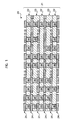
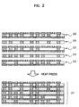
FIG. 1 shows a sectional structure of a multilayer printed
wiring board manufactured by applying a concept of the present
invention; and FIG. 2 shows a status of a stacked-layer thereof.
In FIG. 1, a multilayer printed wiring board 20 has a build-up
board 21 (including a conductive layer on the front surface layer)
of n-layered structure (n is not particularly limited; but it
is assumed that n=5 for convenience) as a main structure body.
Each layer of the build-up board 21 is a double-sided substrate
22 having conductive circuits on both surfaces and a junction
substrate 23 for joining the double-sided substrates 22 to each
other. That is, in an example of the structure shown in FIG.
1, from the lower layer to the upper layer, a double-sided substrate
22, a junction substrate 23, a double-sided substrate 22, a
junction substrate 23, and a double-sided substrate 22 are built
up one after the other in this order. And an integrated build-up
board 21 is obtained by subjecting the above to a heat press
process (refer to FIG. 2).
Hereinafter, for the convenience of explanation, the
double-sided substrate 22 at the lowermost layer will be referred
to as the "first double-sided substrate 22"; likewise, the
junction substrate 23 thereon will be referred to as the "first
junction substrate 23"; the double-sided substrate 22 as an
intermediate layer will be referred to as the "second double-sided
substrate 22"; the junction substrate 23 thereon will be referred
to as the "second junction substrate 23"; and the double-sided
substrate 22 at the uppermost layer will be referred to as the
"third double-sided substrate 22".
On the front and rear surfaces of the first to third
double-sided substrates 22, lower face side conductor circuits
24 and upper face side conductor circuits 25, each of which is
patterned to a desired configuration respectively, are formed.
In the case where a double-sided substrate 22 and a junction
substrate 23 are in contact with each other, the conductor circuits
24 and 25, which are located between the contact faces thereof,
are embedded in the neighboring junction substrates 23. The
reason of the above is as described below. That is, as the main
material for the junction substrates 23, an insulating material,
which has flexibility such as a material of thermosetting type;
for example, an epoxy resin, a cyanate ester resin, a polyphenylene
ether resin, benzo cyclobutene resin, polyimide resin, etc. is
used, and a heat press is carried out after stacking the layers
in the above-described order and the conductor circuits 24 and
25 located between the contact faces enter (embedded) into the
neighboring junction substrates 23. Further, the material for
the junction substrates 23 is not limited to a thermosetting
type insulating material. If the conductor circuits 24 and 25
located between the contact faces are embedded into the
neighboring junction substrates 23, a thermoplastic insulating
material may be employed.
In the first to third double-sided substrates 22 and in the
first and second junction substrates 23, a desired number of
via holes 26 are formed. Each of the via holes 26 ensures
electrical connection between the conductor circuits 24 and 25
on one layer adj acent to the base layer and the conductor circuits
24 and 25 on the other layer. For example, a via hole 26 (refer
to a via hole 26 encircled with a dot line), which is formed
at the right-end of the second double-sided substrate 22, ensures
the electrical connection between one of the lower face side
conductor circuits 25 on the second junction substrate 23 at
the upper layer thereof and one of the upper face side conductor
circuits 24 of the first junction substrate 23 at the lower layer
thereof.
Conventionally, the wording "via hole" is generally
understood as an electrical connection path constituted of a
hole formed in each of the layers of a build-up board which is
"filled with" conductive paste or electrolytic plating
and "hardened" by means of a heat treatment or the like. As will
be clarified by the following description, the via holes 26
according to the embodiment of the present invention is different
from the via hole based on the above described conventional
understanding in a point that the processes of "filling with"
and the "hardening" are not required.
Hereinafter, in order to clarify the above point, description
will be made further in detail.
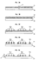
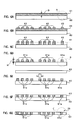
FIG. 3 and FIG. 4 are manufacturing process charts of the
double-sided substrate 22 (the first double-sided substrate 22
to the third double-sided substrate 22).
The process in FIG. 3 (a) : first of all, a sheet-like supporter
30, which can be peeled off, is prepared. On one surface of the
supporter 30 (in FIG. 3 (a), upper surface), metal foil (for example,
copper foil) 31 of good conductivity is laminated. For the
supporter 30, for example, a circuit forming transfer sheet
manufactured by SEKISUI CHEMICAL CO., LTD. may be employed.
Here, assuming that the design height of the via holes 26
to be formed on the double-sided substrate 22 is "H", the thickness
"D" of the metal foil 31 has a value equal to "H". That is, D=H.
Accordingly, for example, when via holes of H=18µm are formed,
metal foil 31 of D=18µm is laminated on the supporter 30.
A process in FIG. 3 (b) : then, the entire surface of the metal
foil 31 is coated with a photosensitive resist 32.
A process in FIG. 3(c): then, exposure and development are
carried out according to the forming pattern of the via holes,
and unnecessary portions of the photosensitive resist 32 is
removed to form etching resists 32a for forming via holes.
Processes in FIGs. 3 (d) and 3(e): then, after carrying out
etching selectively on the metal foil 31 (etching on the portion
where is not coated with the etching resists 32a), unnecessary
etching resists 32a are removed. Thereby, as shown in FIG. 3 (e),
the metal foil 31 is patterned to a desired configuration and
a plurality of columnar metal conductor pieces (hereinafter,
referred to as "columnar conductor") 31a are left on the supporter
30. Being originally formed of the metal foil 31, needless to
say, these columnar conductors 31a have good electrical
conductivity and have a height H equal to the thickness D of
the metal foil 31.
Processes in FIGs. 4 (a) and 4(b): then, one surface of the
supporter 30 (the surface having columnar conductors 31a) is
laminated with a softened sheet-like insulation resin (resin
material) 33 by pressure. Thereby, as shown in FIG. 4(b), the
columnar conductors 31a formed on one surface of the supporter
30 enters (embedded) into the sheet-like insulation resin 33;
and a state where the columnar conductors 31a are "transferred"
to the sheet-like insulation resin 33 is obtained.
A process in FIG. 4 (c) : then, the supporter 30, which becomes
unnecessary by the above-mentioned transfer, is peeled off.
A process in FIG. 4(d): then, on both side surfaces of the
sheet-like insulation resin 33, metal foils 34 and 35 for conductor
circuits (preferably, well-conductivitymetal foil such as copper
foil) are placed and heat pressed to integrate with each other.
A process in FIG. 4(e): finally, each of the metal foils
34 and 35 for conductor circuits is patterned in accordance with
a predetermined conductor circuit pattern to form a desired upper
face side conductor circuit 34a and a lower face side conductor
circuit 35a. Thus, one double-sided substrate 22 is obtained.
When these double-sided substrates 22 are used as the first
double-sided substrate 22 to the third double-sided substrate
22 in FIG. 1, the upper face side conductor circuit 34a and the
lower face side conductor circuit 35a become the upper face side
conductor circuit 25 and the lower face side conductor circuit
24 respectively of the first double-sided substrate 22 to the
third double-sided substrate 22 in FIG. 1. Also, the columnar
conductors 31a transferred to the sheet-like insulation resin
33 become the via holes 26 in the first double-sided substrate
22 to the third double-sided substrate 22 in FIG. 1.
As demonstrated in the above description, in this embodiment,
the via holes 26 in the first double-sided substrate 22 to the
third double-sided substrate 22 are the columnar conductors 31a
themselves that are transferred to the sheet-like insulation
resin 33. Since these columnar conductors 31a are the patterned
metal foil 31, the columnar conductors 31a have electrical well
conductivity, and the height "H" of the columnar conductors 31a
are equal to the thickness "D" of the metal foil 31.
Accordingly, since the processes such as "filling" and
"hardening" are not required, the via holes 26 according to this
embodiment are free from, for example, defective shapes such
as the uneven height of the via holes due to shortage or excess
in filling amount. Thus, the following particular effect is
obtained; i.e., the drawback of the via holes in the conventional
art (refer to the via hole 16 in FIG. 11) is eliminated.
In the manufacturing processes, in the step of process in
FIG. 4(d), the both side surfaces of the sheet-like insulation
resin 33 is laminated with metal foils 34 and 35 for conductor
circuits respectively. However, the present embodiment is not
limited to the above. For example, the processes in FIGs. 4 (a)
to (d) may be modified as described below.
FIG. 5 shows amanufacturingprocess chart of the double-sided
substrate 22 (the first double-sided substrate 22 to the third
double-sided substrate 22), which may be replaced with the
processes in FIGs. 4(a) to 4(d).
Processes in FIGs. 5(a) and 5(b): first of all, one side
surface of the supporter 30 (the surface having the columnar
conductors 31a) is laminated with metal foil 36 with resin
(softened sheet-like insulation resin 33 to which the metal foil
34 conductor circuit is placed before hand) with pressure.
Thereby, as shown in FIG. 5(b), the columnar conductors 31a formed
on one surface of the supporter 30 enters (embedded) into the
sheet-like insulation resin 33, and a state where the columnar
conductors 31a are "transferred" to the sheet-like insulation
resin 33 is obtained.
A process in FIG. 5(c): then, after peeling off the supporter
30, which becomes unnecessary due to the above-described transfer,
on the bottom surface of the sheet-like insulation resin 33,
the metal foil 35 for conductor circuits is pasted and heat pressed
to integrate with each other.
Even in such manner as described above, the double-sided
substrate 22 having the structure in which both surfaces of the
sheet-like insulation resin 33 is laminated with metal foils
34 and 35 for conductor circuits is obtained.
Then, the manufacturing process of the junction substrate
23 will be described. Basically, this manufacturing process is
also the same as that of the double-sided substrate 22. The
essential point of this process is that the via holes can be
formed without requiring the processes of "filling" or
"hardening".
FIG. 6 is a manufacturing process chart of the junction
substrate 23 (the first junction substrate 23 and the second
junction substrate 23).
A process in FIG. 6 (a) : first of all, a sheet-like supporter
60, which is the same as the above-described supporter 30 and
can be peeled off, is prepared. On one surface of the supporter
60 (upper surface in FIG. 6 (a)), metal foil (for example, copper
foil) 61 of good conductivity is placed. Same as the case of
the double-sided substrate 22, assuming that the design height
of the via holes 26 formed in the junction substrate 23 is "H",
the thickness "D" of the metal foil 61 has a value equal to the
"H". That is, D = H. Accordingly, for example, when forming
via holes of H=18µm, metal foil 61 of D=18µm is laminated on
the supporter 60.
A process in FIG. 6(b): then, an etching resist 62 for forming
via holes is formed on the surface of the metal foil 61.
Processes in FIGs. 6(c) and 6(d): then, after selectively
etching on the metal foil 61 (etching on portion where is not
coated with the etching resist 62), unnecessary etching resist
62 is removed. Thereby, as shown in FIG. 6(d), a part of the
metal foil 61 is patterned, and on the supporter 60, a plurality
of columnar metal conductor pieces (hereinafter, referred to
as "columnar conductors") 61a are left. Originally, these
columnar conductors 61a are formed of the metal foil 61. Needless
to say, the columnar conductors 61a have good electrical
conductivity, and have the height "H" equal to the thickness
"D" of the metal foil 61.
Processes in FIGs. 6(e) and 6 (f) : then, one surface of the
supporter 60 (the surface having columnar conductors 61a) is
laminated with a softened sheet-like insulation resin (resin
material) 63 by pressure. Thereby, as shown in FIG. 6(f), the
columnar conductors 61a formed on one surface of the supporter
60 enters (embedded) into the sheet-like insulation resin 63;
and a state where the columnar conductors 61a are "transferred"
to the sheet-like insulation resin 63 is obtained.
A process in FIG. 6(g): finally, the supporter 60, which
becomes unnecessary to the above-mentioned transfer, is peeled
off. Thus, one junction substrate 23 is obtained.
When this junction substrate 23 is applied to the first
junction substrate 23 and the second junction substrate 23 in
FIG. 1, the columnar conductors 61a transferred to the sheet-like
insulation resin 63 become the respective via holes 26 in the
first junction substrate 23 and the second junction substrate
23 in FIG. 1.
As demonstrated in the above description, also in this
embodiment, the via holes 26 in the first junction substrate
23 and the second junction substrate 23 are the columnar conductors
61a themselves transferred to the sheet-like insulation resin
63. Since these columnar conductors 61a are the patterned metal
foil 61, the columnar conductors 61a have good electrical
conductivity, and the height "H" of the columnar conductors 61a
are equal to the thickness "D" of the metal foil 61.
Accordingly, since the processes such as "filling" and
"hardening" are not required, the via holes 26 in the first junction
substrate 23 and the second junction substrate 23 are also free
from, for example, defective shapes such as uneven height of
the via holes due to shortage or excess in filling amount. Thus
the following particular effect is obtained; i.e., the drawback
of the via holes in the conventional art (refer to the via hole
16 in FIG. 11) is eliminated.
The present invention is not limited to the above embodiment.
Needless to say, various modifications within the scope of the
concept of the invention should be included in the present
invention.
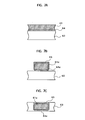
FIG. 7 shows an essential process of an example of a
modification. FIG. 7(a) is an enlarged view of a portion "A"
in FIG. 6(a); FIG. 7(b) is an enlarged view of a portion "B"
in FIG. 6(d); and FIG. 7(c) is an enlarged view of a portion
"C" in FIG. 6(e). Referring to FIG. 7 (a), in this modification,
when laminating the metal foil 61 of well-conductivity on one
surface of the supporter 60, an intermediate layer 64 formed
of a low temperature diffusion metal (for example, tin and the
like) is interposed between the supporter 60 and the metal foil
61. Then, as shown in FIG. 7(b), when selectively etching the
metal foil 61 (process in FIG. 6(c)) to form the columnar conductor
61a, the intermediate layer 64 is also etched simultaneously
to form a bottom face coating portion 64a coating the bottom
face of the columnar conductors 61a. Then, uncoated surfaces
(side surfaces and upper surface) of the columnar conductors
61a are coated with the same metal material as the intermediate
layer 64 (low temperature diffusion metal such as tin) 65. Then,
as shown in FIG. 7(c), by "transferring" the columnar conductors
61a to the sheet-like insulation resin 63 (process in FIG. 6(e)),
the columnar conductor 61a of which periphery are coated with
low temperature diffusion metal (64a, 65) can be embedded in
the sheet-like insulation resin 63.
As a result, at least both end faces (front and rear side
faces of the junction substrate 23) of the columnar conductors
61a, which functions as the via hole 26, are coated with the
low temperature diffusion metal (64a, 65). Accordingly, the
following merit is obtained; i.e., the junction performance
between the conductor circuits (the lower face side conductor
circuit 24 and the upper face side conductor circuit 25) on the
double-sided substrates 22 adjacent to the junction substrate
23 and the via holes 26 in the junction substrate 23 is increased.
FIG. 8 shows an essential process of another example of the
modification; FIG. 8 (a) is an enlarged view of a portion "B"
in FIG. 6(d); and FIG. 8 (b) is an enlarged view of a portion
"C" in FIG. 6(e). Referring to FIG. 8(a), the essential point
of this modification is to carry out "roughening process" as
described below. That is, after selectively etching the metal
foil 61 (process in FIG. 6(c)) to form the columnar conductors
61a, minute concavities and convexities 61b are formed on the
surface of the columnar conductors 61a (in FIG. 8 (a), on the
upper surface and the side surface; but at least, on the side
surface).
Consequently, as shown in FIG.8(b), when the columnar
conductors 61a are embedded in the sheet-like insulation resin
63, the sheet-like insulation resin 63 and the columnar conductors
61a are in contact with each other (refer to portions indicated
with reference symbol "D" in FIG. 8(b)) via the concavities and
convexities 61b on the side surface of the columnar conductors
61a. Due to these concavities and convexities 61b, the
substantial contact area of the both sides is enlarged and the
junction strength between the sheet-like insulation resin 63
and the columnar conductors 61a are increased. As a result,
disadvantages such as peeling-off can be avoided resulting in
an increased reliability.
FIG. 9 shows photographs of the surface of the columnar
conductor 61a for comparing the states before the roughening
process (a) and after the roughening process (b). These
photographs were taken using an SEM (scanning electron
microscope). The photographing conditions in both pictures were
15KV (impressed voltage), ×5000 (magnifications). Comparing
them both, in the case of (a), only smooth waves, which are minute
to a negligible level can be seen; in the case of (b), the entire
surface is filled with minute concavities and convexities, which
are repeated at substantially regular intervals. Obviously, in
the case of (b), effect of the surface roughening can be recognized.
In this modification, the example, in which the columnar
conductor 61a of the junction substrate 23 is roughened, has
been described. However, the present invention is not limited
to the above. The columnar conductors 31a on the double-sided
substrates 22 maybe roughened. Further, as another modification,
when laminating the metal foil 61 of good conductivity on one
surface of the supporter 60, an intermediate layer 64 of low
temperature diffusion metal (for example, tin or the like) is
interposed between the supporter 60 and the metal foil 61. And,
as shown in FIG. 7(b), when selectively etching the metal foil
61 (process in FIG. 6(c)) to form the columnar conductor 61a,
the intermediate layer 64 is also etched simultaneously to form
the bottom face coating portion 64a coating the bottom face of
the columnar conductor 61a. Then, after forming the columnar
conductor 61a, the "roughening process", in which minute
concavities and convexities 61b are formed on the surface of
the columnar conductor 61a, is carried out. Then, the uncoated
surface (side surface and upper surface) of the columnar conductor
61a is coated with the same metal material (low temperature
diffusion metal such as tin) 65 as that of the intermediate layer
64. And, as shown in FIG. 7(c), the columnar conductor 61a is
"transferred" to the sheet-like insulation resin 63 (process
in FIG. 6(e)). Thus, columnar conductors 61a of which periphery
is coated with the low temperature diffusion metal (64a, 65)
can be embedded in the sheet-like insulation resin 63.
Further, as another modification, for example, if necessary,
the front and rear surfaces of the columnar conductors 31a may
be cleaned using permanganic acid or a laser before forming sheet
layer in FIG. 4 (d). Or, when forming the junction substrate 23,
after transferring the columnar conductor 61a to the sheet-like
insulation resin 63, the surface of the columnar conductor 61a
may be cleaned using a laser, etc.
As described above, according to the present invention, the
multilayer printed wiring board and the manufacturing method
thereof are suitable to be used for high density mounting of
electronic parts.
For example, the multilayer printed wiring board and the
manufacturing method thereof may be applied to electronic parts,
semiconductor chips, printed boards, electronic circuits,
modules which are a kind of units or component parts, particularly
to modules in which one or a plurality of semiconductor chips,
resister devices, capacitive elements or other electronic parts
are mounted to achieve an intended electronic circuit function.
Such modules may be applied, for example, to electronic devices,
mobile phones, and mobile information terminals. Further, the
present invention is not limited to the above, but may be widely
applied to electronic parts employing multilayer printed wiring
boards and manufacturing methods thereof capable of utilizing
the effects of the present invention.
The present invention is suitable for high density mounting
of component parts and is capable of readily achieving the
miniaturization of electronic devices and high-speed signal
transmission.
Claims (6)
- A multilayer printed wiring board (20) comprising:a multilayer printed wiring board with an Interstitial Via Hole (IVH) structure in which the main structure is a build-up board (21) composed of a plurality of insulating layers and provided with via holes (16) which electrically interconnect between a conductor circuit of a base layer or adjacent layers in each of said insulating layers; andsaid via holes are formed by patterning metallic foil which is electrically conductive.
- The multilayer printed wiring board (20) according to claim 1, wherein said insulation layers are formed with a resin material; and
said via holes at least undergo roughening treatment of the surface in contact with said resin material. - The multilayer printed wiring board (20) according to claim 1, wherein said via holes at least undergo a coating treatment of the surfaces adjoining said conductor circuit in adjacent layers with low-temperature diffusion metal.
- A manufacturing method of a multilayer printed wiring board (20) in which at the time of manufacturing each layer of a build-up board (21) composed of a multilayer printed wiring board with an Interstitial Via Hole (IVH) structure includes:a first process step which bonds a metallic foil having electrical conductivity on one side of a sheet-like support substrate and supports possible exfoliation;a second process step which forms metallic conductor pieces for said via holes and patterns said metallic foil after said first process;a third process step which transfers saidmetallic conductor pieces to sheet-like insulating resin after said second process; anda fourth process step which exfoliates said support substrate after said third process.
- The manufacturing method of a multilayer printed wiring board (20) according to claim 4 includes a fifth process step in which roughening treatment is performed on the surface of at least said metallic conductor pieces in contact with said insulating resin.
- The manufacturing method of a multilayer printed wiring board (20) according to claim 4 includes a sixth process step in which coating treatment is performed on said metal conductor pieces with low-temperature diffusion metal.
Applications Claiming Priority (3)
| Application Number | Priority Date | Filing Date | Title |
|---|---|---|---|
| JP2002237866 | 2002-08-19 | ||
| JP2002237866A JP2004079773A (en) | 2002-08-19 | 2002-08-19 | Multilayer printed wiring substrate and its production method |
| PCT/JP2003/010049 WO2004017689A1 (en) | 2002-08-19 | 2003-08-07 | Multilayer printed wiring board and production method therefor |
Publications (2)
| Publication Number | Publication Date |
|---|---|
| EP1545176A1 true EP1545176A1 (en) | 2005-06-22 |
| EP1545176A4 EP1545176A4 (en) | 2009-03-04 |
Family
ID=31884446
Family Applications (1)
| Application Number | Title | Priority Date | Filing Date |
|---|---|---|---|
| EP03788053A Withdrawn EP1545176A4 (en) | 2002-08-19 | 2003-08-07 | Multilayer printed wiring board and production method therefor |
Country Status (6)
| Country | Link |
|---|---|
| US (1) | US7278205B2 (en) |
| EP (1) | EP1545176A4 (en) |
| JP (1) | JP2004079773A (en) |
| CN (1) | CN1689382A (en) |
| AU (1) | AU2003254848A1 (en) |
| WO (1) | WO2004017689A1 (en) |
Families Citing this family (12)
| Publication number | Priority date | Publication date | Assignee | Title |
|---|---|---|---|---|
| CN100468706C (en) * | 2003-12-04 | 2009-03-11 | 松下电器产业株式会社 | Circuit board and manufacturing method thereof, semiconductor package and component built-in module |
| JP2007059821A (en) * | 2005-08-26 | 2007-03-08 | Shinko Electric Ind Co Ltd | Wiring board manufacturing method |
| US20160343593A1 (en) * | 2006-05-10 | 2016-11-24 | Amkor Technology, Inc. | Semiconductor package including premold and method of manufacturing the same |
| CN101472404B (en) * | 2007-12-25 | 2011-12-07 | 富葵精密组件(深圳)有限公司 | Multi-layer circuit board and manufacturing method thereof |
| EP2416355B1 (en) * | 2009-04-02 | 2016-12-21 | Murata Manufacturing Co., Ltd. | Circuit board |
| US8161637B2 (en) * | 2009-07-24 | 2012-04-24 | Ibiden Co., Ltd. | Manufacturing method for printed wiring board |
| CN103068172B (en) * | 2012-12-26 | 2015-04-22 | 华映视讯(吴江)有限公司 | Orthobaric pressing printed circuit board support device |
| KR20140134479A (en) * | 2013-05-14 | 2014-11-24 | 삼성전기주식회사 | Printed circuit board |
| JP6450620B2 (en) * | 2015-03-26 | 2019-01-09 | 東京応化工業株式会社 | Substrate peeling apparatus and substrate peeling method |
| JP2016219452A (en) * | 2015-05-14 | 2016-12-22 | 富士通株式会社 | Multilayer substrate and method for manufacturing multilayer substrate |
| CA3076585A1 (en) | 2017-09-29 | 2019-04-04 | Printpack Illinois, Inc. | Packaging material with matte and glossy appearance, and cold seal adhesive |
| CN111491458A (en) * | 2019-01-25 | 2020-08-04 | 鹏鼎控股(深圳)股份有限公司 | Circuit board and manufacturing method thereof |
Family Cites Families (22)
| Publication number | Priority date | Publication date | Assignee | Title |
|---|---|---|---|---|
| US3405227A (en) * | 1966-09-16 | 1968-10-08 | Control Data Corp | Multilayer universal printed circuit board |
| US3488429A (en) * | 1969-02-24 | 1970-01-06 | Gerald Boucher | Multilayer printed circuits |
| JPH04112596A (en) * | 1990-08-31 | 1992-04-14 | Matsushita Electric Ind Co Ltd | Manufacture of multilayer printed wiring board |
| JPH07106761A (en) * | 1993-10-08 | 1995-04-21 | Hitachi Chem Co Ltd | Manufacture of multilayer printed wiring board |
| JPH07142863A (en) * | 1993-11-12 | 1995-06-02 | Matsushita Electric Ind Co Ltd | Multilayer printed wiring board and manufacturing method thereof |
| JP3474913B2 (en) | 1994-03-14 | 2003-12-08 | 株式会社東芝 | Manufacturing method of printed wiring board |
| JP3513827B2 (en) * | 1996-07-01 | 2004-03-31 | 日立化成工業株式会社 | Plastic flow sheet for multilayer printed wiring board and method of manufacturing multilayer printed wiring board using the same |
| JPH1187923A (en) * | 1997-09-11 | 1999-03-30 | Hitachi Chem Co Ltd | Manufacture of multilayered wiring board |
| JPH1187922A (en) * | 1997-09-11 | 1999-03-30 | Hitachi Chem Co Ltd | Manufacture of multilayered wiring board |
| JPH1187921A (en) * | 1997-09-11 | 1999-03-30 | Hitachi Chem Co Ltd | Manufacture of multilayered wiring board |
| JP3988227B2 (en) | 1997-12-01 | 2007-10-10 | 日立化成工業株式会社 | Manufacturing method of semiconductor chip mounting substrate and semiconductor device |
| JPH11204943A (en) | 1998-01-08 | 1999-07-30 | Hitachi Ltd | Electronic circuit board and method of manufacturing the same |
| TW512467B (en) | 1999-10-12 | 2002-12-01 | North Kk | Wiring circuit substrate and manufacturing method therefor |
| JP2001111189A (en) | 1999-10-12 | 2001-04-20 | North:Kk | Wiring circuit board and manufacturing method thereof |
| JP2001326459A (en) | 2000-05-16 | 2001-11-22 | North:Kk | Wiring circuit board and its manufacturing method |
| JP3981227B2 (en) | 1999-12-28 | 2007-09-26 | テセラ・インターコネクト・マテリアルズ,インコーポレイテッド | Multilayer wiring board and manufacturing method thereof |
| JP2001230551A (en) * | 2000-02-14 | 2001-08-24 | Ibiden Co Ltd | Printed wiring board, multil ayered printed wiring board and its manufacturing method |
| JP3636290B2 (en) * | 2000-03-27 | 2005-04-06 | 株式会社東芝 | Printed wiring board and manufacturing method thereof |
| JP4322402B2 (en) * | 2000-06-22 | 2009-09-02 | 大日本印刷株式会社 | Printed wiring board and manufacturing method thereof |
| JP2002050870A (en) * | 2000-08-01 | 2002-02-15 | Hitachi Chem Co Ltd | Connecting substrate, multilayered wiring board and substrate for semiconductor package using it, method of manufacturing semiconductor package and it, method of manufacturing multilayered wiring board using the method, and method of manufacturing substrate for semiconductor package |
| JP3769587B2 (en) | 2000-11-01 | 2006-04-26 | 株式会社ノース | Wiring circuit member, manufacturing method thereof, multilayer wiring circuit board, and semiconductor integrated circuit device |
| JP2002190672A (en) * | 2000-12-19 | 2002-07-05 | Hitachi Metals Ltd | Build-up core board, build-up wiring board, and method of manufacturing the same |
-
2002
- 2002-08-19 JP JP2002237866A patent/JP2004079773A/en active Pending
-
2003
- 2003-08-07 AU AU2003254848A patent/AU2003254848A1/en not_active Abandoned
- 2003-08-07 US US10/525,037 patent/US7278205B2/en not_active Expired - Fee Related
- 2003-08-07 EP EP03788053A patent/EP1545176A4/en not_active Withdrawn
- 2003-08-07 CN CN03823880.2A patent/CN1689382A/en active Pending
- 2003-08-07 WO PCT/JP2003/010049 patent/WO2004017689A1/en not_active Ceased
Also Published As
| Publication number | Publication date |
|---|---|
| CN1689382A (en) | 2005-10-26 |
| WO2004017689A1 (en) | 2004-02-26 |
| AU2003254848A1 (en) | 2004-03-03 |
| US7278205B2 (en) | 2007-10-09 |
| JP2004079773A (en) | 2004-03-11 |
| EP1545176A4 (en) | 2009-03-04 |
| US20060016620A1 (en) | 2006-01-26 |
Similar Documents
| Publication | Publication Date | Title |
|---|---|---|
| CN1115083C (en) | Method for mfg. of printed wiring base plate and printed wiring plate | |
| US7937833B2 (en) | Method of manufacturing circuit board | |
| JP2874329B2 (en) | Method for manufacturing multilayer printed wiring board | |
| US20130319740A1 (en) | Electronic component built-in substrate and method of manufacturing the same | |
| JP2008109140A (en) | Circuit board and manufacturing method thereof | |
| US7278205B2 (en) | Multilayer printed wiring board and production method therefor | |
| US11310922B2 (en) | Board-to-board connecting structure and method for manufacturing the same | |
| JPH11186698A (en) | Circuit board manufacturing method and circuit board | |
| GB2294363A (en) | Flexible multi-layered wiring board | |
| KR100993342B1 (en) | Printed circuit board and manufacturing method thereof | |
| CN103379749A (en) | Multilayer circuit board and manufacturing method thereof | |
| KR100832650B1 (en) | Multilayer printed circuit board and its manufacturing method | |
| KR100701353B1 (en) | Multilayer printed circuit board and its manufacturing method | |
| US20070029109A1 (en) | Multilayer printed wiring board and production method therefor | |
| JP3705370B2 (en) | Manufacturing method of multilayer printed wiring board | |
| US6492007B1 (en) | Multi-layer printed circuit bare board enabling higher density wiring and a method of manufacturing the same | |
| JP2000323841A (en) | Multilayer circuit board and manufacture thereof | |
| KR100441253B1 (en) | method for manufacturing multi-layer printed circuit board using bump | |
| JPH1174640A (en) | Manufacturing method of printed wiring board | |
| EP0572232A2 (en) | A multilayer printed circuit board and method for manufacturing same | |
| JP2004214393A (en) | Method for producing multilayer wiring board | |
| JP4160813B2 (en) | Multilayer circuit board manufacturing method | |
| JP2000133943A (en) | Method for manufacturing multilayer substrate | |
| JP3179564B2 (en) | Multilayer printed wiring board and method of manufacturing the same | |
| JP3238901B2 (en) | Multilayer printed wiring board and method of manufacturing the same |
Legal Events
| Date | Code | Title | Description |
|---|---|---|---|
| PUAI | Public reference made under article 153(3) epc to a published international application that has entered the european phase |
Free format text: ORIGINAL CODE: 0009012 |
|
| 17P | Request for examination filed |
Effective date: 20050216 |
|
| AK | Designated contracting states |
Kind code of ref document: A1 Designated state(s): AT BE BG CH CY CZ DE DK EE ES FI FR GB GR HU IE IT LI LU MC NL PT RO SE SI SK TR |
|
| AX | Request for extension of the european patent |
Extension state: AL LT LV MK |
|
| DAX | Request for extension of the european patent (deleted) | ||
| A4 | Supplementary search report drawn up and despatched |
Effective date: 20090129 |
|
| STAA | Information on the status of an ep patent application or granted ep patent |
Free format text: STATUS: THE APPLICATION IS DEEMED TO BE WITHDRAWN |
|
| 18D | Application deemed to be withdrawn |
Effective date: 20090428 |