EP1540858B1 - Procédé de transmission de signaux optiques multiplexés en polarisation - Google Patents
Procédé de transmission de signaux optiques multiplexés en polarisation Download PDFInfo
- Publication number
- EP1540858B1 EP1540858B1 EP03797242A EP03797242A EP1540858B1 EP 1540858 B1 EP1540858 B1 EP 1540858B1 EP 03797242 A EP03797242 A EP 03797242A EP 03797242 A EP03797242 A EP 03797242A EP 1540858 B1 EP1540858 B1 EP 1540858B1
- Authority
- EP
- European Patent Office
- Prior art keywords
- signal
- signals
- filter
- converted
- optical
- Prior art date
- Legal status (The legal status is an assumption and is not a legal conclusion. Google has not performed a legal analysis and makes no representation as to the accuracy of the status listed.)
- Expired - Lifetime
Links
Images



Classifications
-
- H—ELECTRICITY
- H04—ELECTRIC COMMUNICATION TECHNIQUE
- H04B—TRANSMISSION
- H04B10/00—Transmission systems employing electromagnetic waves other than radio-waves, e.g. infrared, visible or ultraviolet light, or employing corpuscular radiation, e.g. quantum communication
- H04B10/60—Receivers
- H04B10/61—Coherent receivers
-
- H—ELECTRICITY
- H04—ELECTRIC COMMUNICATION TECHNIQUE
- H04J—MULTIPLEX COMMUNICATION
- H04J14/00—Optical multiplex systems
- H04J14/06—Polarisation multiplex systems
Definitions
- the invention relates to a method for transmitting optical polarization multiplex signals according to the preamble of claim 1.
- bit rates of 10 Gbit / s per channel are common today.
- Developed and implemented as a sample were already 40 GBit / s systems.
- PMD polarization mode dispersion
- chromatic dispersion For compensation, a polarization controller and optical compensation devices are used.
- telcom report 1/88 pages 22 to 25 a directional radio system is described which transmits orthogonal polarized signals by means of suitable antennas. Imperfect technical features such as misaligned antennas and reflections lead to cross-polarization perturbations, where one signal interferes with the other, actually orthogonal, signal.
- the polarized signals are separated by separate antennas. Adaptive time domain equalizers are provided to eliminate cross polarization noise.
- the basic idea of a depolarization compensation is to obtain a compensation signal and to the respective main to add. A frequency offset must not occur and time shifts between the signals must be compensated. However, the change in polarization occurring in radio transmission is low compared to optical transmission via fibers. Any polarization can occur here.
- the object of the invention is to achieve an increase in the transmission capacity in the case of optical data transmission without requiring increased bandwidth requirements for optical and electrical system components and further reducing the outlay.
- the combination of four-stage multiphase modulation and polarization-multiplex transmission with the same bandwidth and insignificantly increased signal-to-noise ratio enables a quadrupling of the data rate.
- Two orthogonal polarized multi-phase signals are transmitted, whereby a minimum influence is ensured.
- Synchronous transmission of the orthogonal polyphase signals further minimizes mutual interference.
- Sensitivity to PMD and chromatic dispersion remains the same or only slightly larger than the known lower data rate systems.
- the system can also be used to transmit several data signals with lower parallel.
- synchronous transmission is advantageous because the polarized signals are least likely to interfere with each other.
- a significant advantage of the invention is given by a special embodiment of the method on the receiving side or the receiver. In this case, no more polarization controller is needed.
- An integral part of the receiver is now a multi-dimensional filter that eliminates the need for a polarization controller and additionally compensates signal distortion.
- substantial portions of the receiver including the multi-dimensional filter and the demodulators may be digitally executed.
- a controller for determining the filter coefficients is already being executed digitally.
- FIG. 1 shows an embodiment of the transmitting part of a transmission system for implementing the method according to the invention.
- a data signal DS is converted in a serial-to-parallel converter 1 into four parallel binary signals A, B, C and D.
- four synchronous data streams can be transmitted.
- Two data streams each, A, B and C, D are fed to a DQPSK precoder 2 or 3 (differential quadrature phase shift keying). This takes into account the previous and the current bit pair and converts the differences between the bit pairs into four possible phase changes of 0, 90, 180 and 270 °.
- the modulators 4 and 5 merely show possible embodiments.
- each modulator its upper branch, which generates a phase position of 0 or 180 °, is activated and the lower branch, with which a phase angle of 90 or 270 ° is activated to generate a polyphase signal (QDPSK signal) E.
- the result is phase angles of 45 °, 135 °, 225 ° and 315 °.
- the data streams C and D are used, which are converted in the lower modulator 5 into the QDPSK signal F.
- Two polarization adjusters 7 and 8 ensure that an output signal QPS1 of one modulator 4 is polarized (at least nearly) orthogonal to the output signal QPS2 of the other modulator 5.
- the thus polarized multiphase signals QPS1 and QPS2 are combined in a polarization beam combiner 9 into a polarization multiplex signal PMS, which is transmitted via a transmission fiber 10.
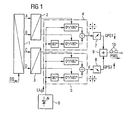
- FIG. 2 is the block diagram of a receiving part for implementing the method according to the invention shown.
- the received polarization multiplex signal PMS is supplied to a polarization splitter 11, which splits it into two orthogonally polarized signal parts PS1 and PS2.
- the first polarized signal part PS1 is supplied to a first optoelectric converter 14; the second polarized signal part PS2 an identically constructed second optoelectric converter 15th
- the polarized signal parts PS1 and PS2 are respectively converted into orthogonal components I 1 , Q 1 and I 2 , Q 2 and fed to a multi-dimensional filter 16. This combines portions of the polarized components into reconstructed signals I 11 + jQ 11 and I 21 + jQ 21 corresponding to the optical signals QPS1; Correspond to QPS2.
- the reconstructed signals I 11 + jQ 11 and I 21 + jQ 21 are demodulated using their orthogonal signal components I 11 and Q 11 or I 21 and Q 21 in the demodulators 17 and 18 and in decision stages 19 -. 22 in reception-side binary signals A E , B E , C E and D E converted back.
- a controller 23 controls the filter 16 and the generation of the clock signals required at the receiving end.
- optical or electrical signals can be processed at the receiving end.
- digitization and digital processing are possible, according to the translators.
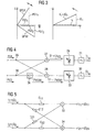
- FIG. 3 shows in its left part signals at the input and at the outputs of the polarization splitter 11.
- the polarization multiplex signal PMS with its two orthogonally polarized multiphase signals QPS1 and QPS2 is applied to the input of the polarization splitter.
- Each signal QPS1 and QPS2 is divided by the polarization divider 11 into a first "vertical" signal component PS1 1 and into a second "horizontal" signal component QS1 1 or PS1 2 and QS1 2, respectively.
- the vertical components form the polarized signal part PS1 and the horizontal polarized signal part PS2.
- Each signal part thus contains portions of both polyphase signals QPS1 and QPS2.
- the "perpendicular" polarized signal part PS1 is applied to the input of the upper opto-electrical converter 14, and the "horizontally” polarized signal part PS2 is applied to the input of the lower opto-electrical converter 15 ( FIG. 2 ).
- the principal function of this opto-electrical (o / e) converter is to convert the polarized sub-signals linearly into a complex electrical signal.
- the implemented converters each output two orthogonal components I 1 and Q 1 or I 2 and Q 2 (Q - imaginary part in the case of complex representation).
- the orthogonal components can be processed more easily.
- a transformation into the baseband of the signal modulating the carrier expediently takes place.
- the optical signal is linearly transformed from the optical domain to the complex baseband plane; the subsequent electrical signal processing is then equivalent to a processing of the optical signal.
- a signal L ⁇ E of a receiving-side carrier frequency generator (laser) is used.
- each converter is supplied to the opto-electrical conversion except the polarized signal part PS1 or PS2 each still a same polarized receiving side carrier frequency signal L ⁇ ES and L ⁇ EW , which has at least approximately the frequency of the carrier signal L ⁇ 0 in this embodiment.
- Each converter includes splitters 35, 36 for dividing the input signals, a phase shifter element 26, two adders 27, 28, photodiodes 29, 30 and low passes 31, 32.
- the polarized signal PS1 is fed via the splitter to both adders 27 and 28 as an input signal.
- the laser signal L ⁇ ES is also divided into two sub-signals, a part of which is added directly to the signal PS1 in the first adder 27.
- a signal L ⁇ ES90 phase-shifted by 90 ° is added.
- the first and the last term of the multiplied sum of formula 1 contain high-frequency vibrations that are removed by the low-pass filter.
- the middle term contains a signal component that has been transformed into a lower frequency position. This signal component is filtered out as electrical component I 1 . Accordingly, the lower electrical component Q 1 is obtained with the signal L ⁇ ES90 phase-shifted by 90 °.
- the receive-side carrier frequency signal L ⁇ E has the frequency of the carrier, so that the transformation into the baseband takes place. If only the frequency of the controlled carrier frequency oscillator 12 but not its phase is controlled, the phase between the carrier of the input signal, the signal part PS1, and L ⁇ ES of the opto-electrical converter changes in a finite control error. As a result, in the case of the complex output signal I 1 + jQ 1 , the phase also changes and it experiences a slow rotation. Accordingly, the amplitudes of the components I 1 , Q 1 also change . As a result, the complex output signals I 11 + jQ 11 and I 21 + jQ 21 of the filter then also rotate about the zero point of the complex plane.
- the output signals I 1 , Q 1 and I 2 , Q 2 have only an orientation dependent on the polarization. Since this is largely compensated by the filter, the angles of the reconstructed signals I 11 + jQ 11 and I 21 + jQ 21 remain largely constant at the filter outputs.
- FIG. 5 shows a simplified complex representation of the filter 16.
- This filter makes it possible to multiply each input signal with a filter coefficient and switch through to each output, the signal components thus generated are added. Since the polarization multiplex signal PMS can have any polarization, the polarized component signals PS1 and PS2 also contain both portions of the first polyphase signal QPS1 and of the second multiphase signal QPS2.
- the controllable filter 16 assumes the task of a polarization controller to reconstruct the polyphase signals QPS1 and QPS2 in the electrical plane from the corresponding electrical signal components I 1 , Q 1 and I 2 , Q 2 .
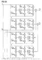
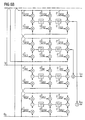
- FIG. 2 shows a block diagram of a transversal filter 16 for processing orthogonal electrical components with which the polyphase signals QPS1 and QPS2 in the electrical plane are to be reconstructed.
- the electrical components I 1 , Q 1 and I 2 , Q 2 are supplied to the multi-dimensional filter 16. Since four signal components each have to be processed and output, this is a four-dimensional filter that has four inputs and four outputs.
- the design of the filter makes it possible to multiply all input signals with arbitrary filter coefficients and additively switch through to each of the four outputs. Due to the "fractional spacing" used, asynchronous polyphase signals can also be processed.
- the output at the output of the filter 16 orthogonal reconstructed signal components I 11 , Q 11 and I 21 , Q 21 respectively correspond - apart from the opto-electrical conversion and rotation - the quadrature phase signals QPS1 and QPS2.
- the reconstructed signal I 11 + jQ 11 or its orthogonal signal components I 11 , Q 11 are supplied to the first demodulator 17, while the reconstructed signal components I 21 , Q 21 are supplied to the second demodulator 18.
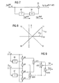
- FIG. 7 shows a simplified schematic diagram of a complex demodulator. This contains a delay element 37 and an arithmetic circuit 38 arranged therewith in series for forming the complex conjugate value and a multiplier 45.
- the demodulation is based on the principle of vector multiplication of two successive symbols.
- the phase values can vary between 0 and 270 °, but in the ideal case they assume the values 0 °, 90 °, 180 °, 270 °.
- the result is rotated by 45 ° by multiplication by (1 + j).
- the individual component is then assigned a bit in each case, which is determined in each case by one of the separate threshold decision 19 - 22.
- FIG. 8 shows the positions of the demodulated signal at different bit combinations A, B.
- a current bit combination "11" is shown by solid lines, the other bit combinations 10, 01, 00 are shown in dashed lines. It can be seen that the thresholds of the decider stages 19-22 coincide with the axbox.
- Each of these demodulators thus provides independent of the location of the input signals independent results, the slow rotation of the input signals can be neglected.
- Each demodulator already supplies components I 12 , Q 12 and I 22 and Q 22 of the demodulated signals I 12 + JQ 12 and I 22 + JQ 22, respectively.
- Two orthogonal signal components each correspond to a bit combination.
- FIG. 9 shows a schematic diagram of the demodulator 17 for processing orthogonal components I 11 and Q 11 , the be fed to its entrances.
- the required mathematical operations are performed on the real and imaginary signal portions of the current and previous orthogonal components as shown.
- Two delay elements 46 and 47 store the previous signal components. After multiplication of the components in the multipliers M, sum values are formed by the adders AD1 and AD2 and difference values from the subtractors SUB1 and SUB2 to obtain the components I 12 and Q 12 of the demodulated signal.
- the decision stages 19 -22 allow after FIG. 2 directly a conversion of the demodulated signal components I 12 , Q 12 , I 22 , Q 22 in the receiving side binary signals A E , B E , C E and D E corresponding to the transmitting side binary signals A, B, C, D.
- the controller 23 (COR correlation, COM compensation) is provided. This also has a carrier frequency controller 24 which controls the receiving side carrier frequency oscillator 12. It also includes a decoder clock regenerator 25.
- the orthogonal signal components I 11 , Q 11 , I 21 , Q 21 or / and the demodulated signal components I 12 , Q 12 ; I will be 22 , Q 22 .
- the errors are minimized by varying the filter coefficients.
- FIG. 10 is an arrangement for obtaining the filter coefficients based on the "minimum mean-square error" (MMSE).
- MMSE minimum mean-square error
- This digitally operating arrangement first converts the analog signal components I 1 , Q 1 , I 2 , Q 2 , I 11 , Q 11 , I 21 , Q 21 into digital signals by means of analog-digital converters ADW.
- ADW analog-digital converters
- the orthogonal component I 1 is delayed by delay elements D several times according to the delay elements of the multi-dimensional filter 16. Each output of the delay elements D is connected to a respective multiplier M. The second inputs of the multipliers an error signal e I11 is supplied.
- This error signal and that of the associated orthogonal component can be determined from error signals e I12 and e Q12 of the demodulated signal components.
- the errors e I 12 and j e Q 12 are first determined in evaluation circuits B.
- the errors of the orthogonal signal component I 11 , Q 11 and I 21 , Q 21 are required. This is obtained by reversing the multiplication carried out in the modulator with the preceding complex conjugate signal value in an arithmetic circuit CU, ie multiplying again by the previous signal value.
- Transducers 14 and 15 is an analog-to-digital conversion by the analog-to-digital converter 41-44.
- the further signal processing takes place digitally with the aid of a clock signal CL.
- the filter 16 and the demodulators are replaced by digitally operating circuits D16, D17, D18.
- this realization is not yet economical due to the high data rates.
- the controllable filter 16 can also be implemented as an optical filter. It would be ideal if the converters are likewise embodied purely optically and emit an amplitude-modulated optical signal.
- the controller can determine the signal quality beyond its already described functions. Numerous methods are known for this, which are based, for example, on different decision thresholds for generating amplitude histograms. Likewise, an error correcting device can provide relevant statements. Causes of poor signal quality are often signal distortions due to the transmission fiber, such as chromatic dispersion and polarization mode dispersion. Since the optoelectric signal conversion was linear, an equivalent electrical equalization can also take place. This too is done by coefficient control of the filter 16.
- a correspondingly modified receiving part can also be used with other types of modulation.
Landscapes
- Engineering & Computer Science (AREA)
- Computer Networks & Wireless Communication (AREA)
- Signal Processing (AREA)
- Physics & Mathematics (AREA)
- Electromagnetism (AREA)
- Digital Transmission Methods That Use Modulated Carrier Waves (AREA)
- Optical Communication System (AREA)
Abstract
Claims (15)
- Procédé pour la transmission de signaux optiques de multiplexage en polarisation, dans lequel au moins un premier signal binaire (A, B) est converti en un premier signal (QPS1) optique et au moins un second signal binaire (D, C) en un second signal optique (QPS2) polarisé orthogonalement par rapport au premier, et les signaux optiques (QPS1, QPS2) polarisés orthogonalement sont assemblés ensuite pour former un signal de multiplexage en polarisation (PMS) et sont transmis ensuite,
caractérisé en ce que,
côté réception, le signal de multiplexage en polarisation (PMS) est subdivisé en deux parties de signal (PS1, PS2) polarisées orthogonalement,
en ce que chaque partie de signal (PS1 ; PS2) polarisée est convertie linéairement en un signal (I1 + jQ1 ; I2 + jQ2) complexe,
les signaux (I1 + jQ1 ; I2 + jQ2) complexes sont amenés à un filtre (16) multidimensionnel, dont les coefficients (Cii) sont commandés de telle sorte que
sont délivrés sur les sorties de filtre des signaux (I11 + jQ11 ; I12 + jQ12) reconstitués, qui correspondent aux signaux (QPS1, QPS2) optiques, indépendamment de la polarisation du signal de multiplexage en polarisation (PMS) reçu et
en ce que les signaux (I11 + jQ11 ; I21 + jQ21) reconstitués sont démodulés et sont convertis en signaux binaires (AE, BE ; CE, DE) côté réception. - Procédé selon la revendication 1,
caractérisé en ce que
chaque partie de signal (PS1 ; PS2) polarisée est convertie linéairement en un signal (I1+ jQ1 ; I2 + jQ2) électrique, complexe et présentant deux composantes (I1, Q1 ; I2, Q2) orthogonales,
en ce que ses composantes (I1, Q1 ; I2, Q2) orthogonales sont amenées au filtre (16) multidimensionnel commandable, qui, à partir de ces composantes (I1, Q1 ; I2, Q2) orthogonales, obtient les signaux (I11 + jQ11 ; I12 + jQ12) reconstitués sous la forme de composantes de signal (I11, Q11 ; I21, Q21) reconstituées. - Procédé selon la revendication 2,
caractérisé en ce que
les parties de signal (PS1, PS2) polarisées sont converties dans les signaux (I1, Q1 ; I2, Q2) complexes resp. les composantes (I1, Q1 ; I2, Q2) orthogonales de la bande de base. - Procédé selon la revendication 1 ou 2,
caractérisé en ce que
les signaux binaires (A, B ; C, D) sont convertis en signaux multiphases (QPS1 ; QPS2) optiques. - Procédé selon la revendication 1 ou 2,
caractérisé en ce que
respectivement deux signaux binaires (A, B ; C, D) sont convertis en signaux multiphases (QPS1 ; QPS2) par modulation de phase différentielle à 4 niveaux. - Procédé selon la revendication 4 ou 5,
caractérisé en ce que,
avec une modulation à quatre phases ou avec une modulation de phase différentielle à quatre niveaux, des composantes de signal (I12, Q12 ; I22, Q22) démodulées sont générées par démodulation des signaux (I12 + jQ12 ; I22 + jQ22) reconstitués ou de leurs composantes de signal (I11, Q11 ; I12, Q12) et
en ce que les composantes de signal (I12, Q12 ; I22, Q22) des signaux (I12 + jQ12, I22 + jQ22) démodulés sont évaluées séparément par des décisions de valeur seuil et sont converties en signaux binaires (AE, BE, CE, DE) côté réception. - Procédé selon la revendication 5,
caractérisé en ce que,
avec une modulation de phase différentielle à quatre niveaux, est effectué une démodulation par multiplication vectorielle de valeurs de signal (I11 + jQ11, I21 + j jQ21) reconstituées consécutives resp. de leurs composantes de signal (I11, Q11 ; I21, Q21) ,
en ce que les valeurs de signal (I12 + j Q12, I22 + j Q22) démodulées sont tournées de 45° ou d'un multiple de ce chiffre et
en ce que les composantes de signal (I12, Q12 ; I22, Q22) correspondants sont converties par des décisions de valeur seuil en signaux binaires (AE, BE, CE, DE) côté réception. - Procédé selon l'une quelconque des revendications précédentes,
caractérisé en ce que
un signal de données (DS) de débit de données supérieur est converti par conversion série-parallèle en plusieurs signaux binaires (A, B, C, D). - Procédé selon l'une quelconque des revendications précédentes,
caractérisé en ce que
les signaux optiques (QPS1, QPS2) sont transmis de façon synchrone en phase. - Procédé selon la revendication 5,
caractérisé en ce que
les coefficients de filtre (Cii) du filtre (16) multidimensionnel sont obtenus à partir des erreurs (eI11 et eQ11, ...) des signaux (I11 + jQ11, ...) démodulés. - Procédé selon la revendication 5,
caractérisé en ce que
les coefficients de filtre du filtre (16) multidimensionnel sont obtenus à partir des erreurs (eI12 et eQ12, ...) des signaux (I12 + jQ12, ...) décodés. - Procédé selon l'une quelconque des revendications précédentes,
caractérisé en ce que
la qualité de signal est mesurée et des distorsions de signal des signaux complexes et/ou des signaux (I1 + jQ1 ; I2 + jQ2 ; I11 + jQ11 ; I21 + j Q21) reconstitués sont compensées. - Procédé selon l'une quelconque des revendications précédentes,
caractérisé en ce que
les distorsions de signal sont compensées par la commande des coefficients de filtre (Cii) du filtre (16). - Procédé selon l'une quelconque des revendications précédentes,
caractérisé en ce que
les composantes (I1, Q1 ; I2, Q2) orthogonales sont traitées dans une forme numérisée dans un filtre (D16) numérique commandable pour obtenir les signaux (I11 + j Q11, I21 + jQ21) reconstitués. - Procédé selon l'une quelconque des revendications précédentes,
caractérisé en ce que
les composantes (I1, Q1 ; I2, Q2) orthogonales sont traitées sous forme de signaux optiques dans un filtre (O16) optique commandable pour obtenir des signaux (I11 + jQ11 ; I21 + j Q21) reconstitués optiques.
Applications Claiming Priority (3)
| Application Number | Priority Date | Filing Date | Title |
|---|---|---|---|
| DE10243141 | 2002-09-17 | ||
| DE10243141A DE10243141B4 (de) | 2002-09-17 | 2002-09-17 | Verfahren zur Übertragung von optischen Polarisationsmultiplexsignalen |
| PCT/EP2003/008997 WO2004028046A1 (fr) | 2002-09-17 | 2003-08-13 | Procede de transmission de signaux multiplex de polarisation optique |
Publications (3)
| Publication Number | Publication Date |
|---|---|
| EP1540858A1 EP1540858A1 (fr) | 2005-06-15 |
| EP1540858B1 true EP1540858B1 (fr) | 2008-10-29 |
| EP1540858B9 EP1540858B9 (fr) | 2010-02-17 |
Family
ID=31969161
Family Applications (1)
| Application Number | Title | Priority Date | Filing Date |
|---|---|---|---|
| EP03797242A Expired - Lifetime EP1540858B9 (fr) | 2002-09-17 | 2003-08-13 | Procédé de transmission de signaux optiques multiplexés en polarisation |
Country Status (9)
| Country | Link |
|---|---|
| US (1) | US7509054B2 (fr) |
| EP (1) | EP1540858B9 (fr) |
| CN (1) | CN100472985C (fr) |
| AU (1) | AU2003253410B2 (fr) |
| CA (1) | CA2499091C (fr) |
| DE (2) | DE10243141B4 (fr) |
| ES (1) | ES2316863T3 (fr) |
| RU (1) | RU2320090C2 (fr) |
| WO (1) | WO2004028046A1 (fr) |
Families Citing this family (34)
| Publication number | Priority date | Publication date | Assignee | Title |
|---|---|---|---|---|
| DE102004047028A1 (de) * | 2004-09-28 | 2006-04-20 | Siemens Ag | Verfahren und Anordnung zur optischen Übertragung von Datensignalen mittels differentieller Phasenmodulation in einem Polarisations-Multiplexverfahren |
| AU2006208719B2 (en) * | 2005-01-26 | 2009-05-28 | Xieon Networks S.A.R.L. | Method for optically transmitting polarisation multiplex signals |
| DE102005003681A1 (de) * | 2005-01-26 | 2006-08-10 | Siemens Ag | Verfahren zur optischen Datenübertragung mit Polarisations- und Wellenlängen-Multiplex |
| US7809284B2 (en) * | 2006-06-23 | 2010-10-05 | Alcatel-Lucent Usa Inc. | System and method for receiving coherent, polarization-multiplexed optical signals |
| US7747169B2 (en) * | 2006-12-22 | 2010-06-29 | Alcatel-Lucent Usa Inc. | Adaptive polarization tracking and equalization in coherent optical receivers |
| EP1942590A1 (fr) * | 2007-01-03 | 2008-07-09 | Alcatel Lucent | Récepteur optique cohérent et procédé pour compensation de la distorsion liée à la polarisation des signaux dans un système de transmission à fibre optique |
| CN101453268B (zh) * | 2007-12-06 | 2013-11-06 | 北京高光科技有限公司 | 基于偏振复用技术的光学通信系统及其方法 |
| US8249463B2 (en) * | 2007-12-07 | 2012-08-21 | Infinera Corporation | Skew compensation across polarized optical channels |
| EP2071754B1 (fr) | 2007-12-10 | 2010-02-10 | Alcatel Lucent | OFDM optique multiplexé en polarisation |
| CN101505192B (zh) | 2008-02-04 | 2011-09-21 | 华为技术有限公司 | 一种产生差分正交相移键控码光信号的方法及装置 |
| US8238758B2 (en) * | 2008-02-22 | 2012-08-07 | Infinera Corporation | Three-arm DQPSK modulator |
| CN101753252B (zh) * | 2008-12-01 | 2013-01-23 | 华为技术有限公司 | 一种光收发方法、装置及系统 |
| JP5195677B2 (ja) * | 2009-07-28 | 2013-05-08 | 富士通株式会社 | 光信号送信装置および偏波多重光信号の制御方法 |
| EP2375603B1 (fr) * | 2010-02-05 | 2018-05-23 | Xieon Networks S.à r.l. | Procédé de récupération d'horloge et agencement de récupération d'horloge pour les récepteurs à multiplexage par polarisation cohérente |
| US8391726B2 (en) * | 2010-02-25 | 2013-03-05 | Futurewei Technologies, Inc. | Method and apparatus for frame detection and polarization separation |
| JP5760419B2 (ja) * | 2010-12-13 | 2015-08-12 | 富士通株式会社 | 光送信装置および光送信方法 |
| JP5120507B2 (ja) * | 2011-02-01 | 2013-01-16 | 日本電気株式会社 | 光受信器、偏光分離装置および偏光分離方法 |
| EP2685642B1 (fr) | 2011-05-31 | 2016-08-31 | Huawei Technologies Co., Ltd. | Procédé et dispositif de traitement de signaux optiques |
| US8873953B2 (en) * | 2011-06-17 | 2014-10-28 | Nec Laboratories America, Inc. | Multiple-symbol polarization switching for differential-detection modulation formats |
| WO2012106921A1 (fr) * | 2011-07-25 | 2012-08-16 | 华为技术有限公司 | Procédé de compensation non linéaire, dispositif et système de réception de signal |
| US9281915B2 (en) * | 2013-01-17 | 2016-03-08 | Alcatel Lucent | Optical polarization demultiplexing for a coherent-detection scheme |
| US9106503B1 (en) * | 2014-06-18 | 2015-08-11 | Futurewei Technologies, Inc. | Method and apparatus for recovering time-domain hybrid modulated QAM signals |
| FI4002724T3 (fi) | 2015-12-13 | 2025-09-30 | Gxc Llc | Häiriönpoistomenetelmiä ja -laite |
| US10257746B2 (en) | 2016-07-16 | 2019-04-09 | GenXComm, Inc. | Interference cancellation methods and apparatus |
| CN106597662B (zh) * | 2016-12-05 | 2019-06-14 | 上海无线电设备研究所 | 一种太赫兹收发共用双极化准光环形器 |
| US11150409B2 (en) | 2018-12-27 | 2021-10-19 | GenXComm, Inc. | Saw assisted facet etch dicing |
| US10727945B1 (en) | 2019-07-15 | 2020-07-28 | GenXComm, Inc. | Efficiently combining multiple taps of an optical filter |
| US11215755B2 (en) | 2019-09-19 | 2022-01-04 | GenXComm, Inc. | Low loss, polarization-independent, large bandwidth mode converter for edge coupling |
| US11539394B2 (en) | 2019-10-29 | 2022-12-27 | GenXComm, Inc. | Self-interference mitigation in in-band full-duplex communication systems |
| US11796737B2 (en) | 2020-08-10 | 2023-10-24 | GenXComm, Inc. | Co-manufacturing of silicon-on-insulator waveguides and silicon nitride waveguides for hybrid photonic integrated circuits |
| US12001065B1 (en) | 2020-11-12 | 2024-06-04 | ORCA Computing Limited | Photonics package with tunable liquid crystal lens |
| WO2022178182A1 (fr) | 2021-02-18 | 2022-08-25 | GenXComm, Inc. | Maximisation de l'efficacité de systèmes de communication avec des sous-systèmes d'annulation d'auto-interférences |
| EP4331120A1 (fr) | 2021-04-29 | 2024-03-06 | Genxcomm, Inc. | Sous-systèmes d'annulation d'auto-interférence pour noeuds de réseau maillé |
| US11838056B2 (en) | 2021-10-25 | 2023-12-05 | GenXComm, Inc. | Hybrid photonic integrated circuits for ultra-low phase noise signal generators |
Family Cites Families (12)
| Publication number | Priority date | Publication date | Assignee | Title |
|---|---|---|---|---|
| US5008958A (en) | 1988-01-19 | 1991-04-16 | At&T Bell Laboratories | Polarization-insensitive technique for coherent optical communication |
| US5060312A (en) * | 1990-03-05 | 1991-10-22 | At&T Bell Laboratories | Polarization independent coherent lightwave detection arrangement |
| US5388088A (en) * | 1992-04-02 | 1995-02-07 | At&T Corp. | Multiple polarization sensitive detection arrangement for fiber optic communications |
| NL9200748A (nl) * | 1992-04-23 | 1993-11-16 | Nederland Ptt | Optische signaaloverdracht met polarisatie-ongevoelige coherente detectie en frekwentiestabilisatie aan de ontvangstzijde. |
| CN1274494A (zh) * | 1997-08-08 | 2000-11-22 | 乔拉姆技术公司 | 多波长交叉连接光纤网 |
| JPH1188260A (ja) * | 1997-09-09 | 1999-03-30 | Fujitsu Ltd | 光伝送路の分散補償装置 |
| US6782211B1 (en) | 1998-11-05 | 2004-08-24 | Mark T. Core | Cross polarization interface canceler |
| KR100317807B1 (ko) * | 1999-03-19 | 2001-12-22 | 서평원 | 편광변조를 이용한 광신호 채널정보 감지장치 및 방법 |
| JP4294153B2 (ja) * | 1999-04-12 | 2009-07-08 | 富士通株式会社 | 波長多重光伝送システム |
| RU2155449C1 (ru) * | 1999-10-22 | 2000-08-27 | Александровский Михаил Исаакович | Линия передачи цифрового оптического сигнала |
| US7076169B2 (en) * | 2000-09-26 | 2006-07-11 | Celight, Inc. | System and method for orthogonal frequency division multiplexed optical communication |
| DE10156244A1 (de) * | 2001-11-15 | 2003-06-05 | Siemens Ag | Anordnung und Verfahren für eine optische Informationsübertragung |
-
2002
- 2002-09-17 DE DE10243141A patent/DE10243141B4/de not_active Expired - Fee Related
-
2003
- 2003-08-13 US US10/528,313 patent/US7509054B2/en not_active Expired - Lifetime
- 2003-08-13 DE DE50310713T patent/DE50310713D1/de not_active Expired - Lifetime
- 2003-08-13 WO PCT/EP2003/008997 patent/WO2004028046A1/fr not_active Ceased
- 2003-08-13 RU RU2005111249/09A patent/RU2320090C2/ru not_active IP Right Cessation
- 2003-08-13 EP EP03797242A patent/EP1540858B9/fr not_active Expired - Lifetime
- 2003-08-13 CN CN03822093.8A patent/CN100472985C/zh not_active Expired - Lifetime
- 2003-08-13 ES ES03797242T patent/ES2316863T3/es not_active Expired - Lifetime
- 2003-08-13 CA CA2499091A patent/CA2499091C/fr not_active Expired - Fee Related
- 2003-08-13 AU AU2003253410A patent/AU2003253410B2/en not_active Ceased
Also Published As
| Publication number | Publication date |
|---|---|
| WO2004028046A1 (fr) | 2004-04-01 |
| RU2005111249A (ru) | 2006-01-20 |
| DE10243141A1 (de) | 2004-04-01 |
| CN1682472A (zh) | 2005-10-12 |
| ES2316863T3 (es) | 2009-04-16 |
| EP1540858B9 (fr) | 2010-02-17 |
| EP1540858A1 (fr) | 2005-06-15 |
| AU2003253410A1 (en) | 2004-04-08 |
| DE50310713D1 (de) | 2008-12-11 |
| AU2003253410B2 (en) | 2008-04-17 |
| CN100472985C (zh) | 2009-03-25 |
| DE10243141B4 (de) | 2006-05-11 |
| CA2499091A1 (fr) | 2004-04-01 |
| US20050286904A1 (en) | 2005-12-29 |
| US7509054B2 (en) | 2009-03-24 |
| CA2499091C (fr) | 2013-11-19 |
| RU2320090C2 (ru) | 2008-03-20 |
Similar Documents
| Publication | Publication Date | Title |
|---|---|---|
| EP1540858B1 (fr) | Procédé de transmission de signaux optiques multiplexés en polarisation | |
| DE69101568T2 (de) | Kreuzpolarisationsinterferenzkompensator. | |
| DE69024148T2 (de) | Übertragungssystem mit Doppelpolarisation | |
| EP0244779B1 (fr) | Compensateur d'interférence de déplorisation adaptif | |
| DE3040685A1 (de) | Phasenzitterkompensation unter verwendung periodischer, harmonisch in beziehung stehender signalkomponeten | |
| DE102006030915B4 (de) | Optischer Empfänger für den Empfang eines Signales mit M-wertiger sternförmiger Quadratur-Amplitudenmodulation mit differenzieller Phasenkodierung und dessen Verwendung | |
| DE2503595A1 (de) | Datenempfaenger fuer synchrone quadraturamplituden-modulierte datensignale | |
| DE3739484C2 (fr) | ||
| DE2646255A1 (de) | Digitales detektorsystem fuer differentielle phasenshift-umtastsignale | |
| WO2003096584A1 (fr) | Procede et dispositif pour limiter la degradation de signal d'un signal multiplexe en polarisation optique | |
| DE60225852T2 (de) | Optische Phasenmodulation | |
| EP1797654B1 (fr) | Procede et dispositif de transmission optique de signaux de donnees par modulation de phase differentielle dans un procede de multiplexage de polarisation | |
| DE2317597C3 (de) | Verfahren und Schaltungsanordnung zum Entzerren eines nach Übertragung mittels Phasenmodulation mit linearen Verzerrungen behafteten Signals vor der Demodulation | |
| DE4110138C1 (en) | Carrier recovery for optical PSK homodyne receiver - by rotating local oscillator phase 90 deg. for one synchronisation bit period to produce phase error signal | |
| EP0401557A2 (fr) | Procédé pour réaliser une réception hétérodyne optique insensible à la phase et/ou à la polarisation d'un signal modulé en sauts de fréquence | |
| DE2416058B2 (de) | Verfahren und Schaltungsanordnungen zur Entzerrung eines quadraturmodulierten Datensignals | |
| EP2903184B1 (fr) | Convertisseur de longueur d'onde et procédé de conversion de longueur d'onde | |
| EP0280075A2 (fr) | Récepteur optique à diversité de polarisation | |
| EP1083717B1 (fr) | Contrôle de la phase d'un oscillateur local dans un récepteur cohérent, optique et homodyne pour signaux MDP | |
| DE2845210A1 (de) | Verfahren und anordnung fuer die bestimmung des phasenschnittpunktes in einem system mit phasenumtastmodulation | |
| DE60026298T2 (de) | Verfahren und vorrichtung zur entzerrung von linear verzerrten signalen | |
| DE3416038A1 (de) | Nachrichtenuebertragungsverfahren der telegraphie | |
| WO1999007099A2 (fr) | Dispositif pour produire rapidement et numeriquement un signal numerique a angle de phase pouvant etre predetermine, au moyen d'un signal porteur de reference | |
| DE10242915A1 (de) | Verfahren und Anordnung zur Verringerung der Signaldegradation eines optischen Polarisation-Multiplexsignals |
Legal Events
| Date | Code | Title | Description |
|---|---|---|---|
| PUAI | Public reference made under article 153(3) epc to a published international application that has entered the european phase |
Free format text: ORIGINAL CODE: 0009012 |
|
| 17P | Request for examination filed |
Effective date: 20050124 |
|
| AK | Designated contracting states |
Kind code of ref document: A1 Designated state(s): AT BE BG CH CY CZ DE DK EE ES FI FR GB GR HU IE IT LI LU MC NL PT RO SE SI SK TR |
|
| AX | Request for extension of the european patent |
Extension state: AL LT LV MK |
|
| DAX | Request for extension of the european patent (deleted) | ||
| RBV | Designated contracting states (corrected) |
Designated state(s): DE ES FR GB IT |
|
| RIN1 | Information on inventor provided before grant (corrected) |
Inventor name: HECKER, NANCY Inventor name: SPINNLER, BERNHARD Inventor name: CALABRO, STEFANO Inventor name: SEBALD, GEORG Inventor name: GOTTWALD, ERICH |
|
| RAP1 | Party data changed (applicant data changed or rights of an application transferred) |
Owner name: NOKIA SIEMENS NETWORKS GMBH & CO. KG |
|
| RAP3 | Party data changed (applicant data changed or rights of an application transferred) |
Owner name: NOKIA SIEMENS NETWORKS S.P.A. |
|
| RTI1 | Title (correction) |
Free format text: METHOD FOR THE TRANSMISSION OF POLARISATION MULTIPLEXED OPTICAL SIGNALS |
|
| RAP3 | Party data changed (applicant data changed or rights of an application transferred) |
Owner name: NOKIA SIEMENS NETWORKS GMBH & CO. KG |
|
| GRAP | Despatch of communication of intention to grant a patent |
Free format text: ORIGINAL CODE: EPIDOSNIGR1 |
|
| GRAC | Information related to communication of intention to grant a patent modified |
Free format text: ORIGINAL CODE: EPIDOSCIGR1 |
|
| GRAS | Grant fee paid |
Free format text: ORIGINAL CODE: EPIDOSNIGR3 |
|
| GRAA | (expected) grant |
Free format text: ORIGINAL CODE: 0009210 |
|
| AK | Designated contracting states |
Kind code of ref document: B1 Designated state(s): DE ES FR GB IT |
|
| REG | Reference to a national code |
Ref country code: GB Ref legal event code: FG4D Free format text: NOT ENGLISH |
|
| REF | Corresponds to: |
Ref document number: 50310713 Country of ref document: DE Date of ref document: 20081211 Kind code of ref document: P |
|
| REG | Reference to a national code |
Ref country code: ES Ref legal event code: FG2A Ref document number: 2316863 Country of ref document: ES Kind code of ref document: T3 |
|
| PLBE | No opposition filed within time limit |
Free format text: ORIGINAL CODE: 0009261 |
|
| STAA | Information on the status of an ep patent application or granted ep patent |
Free format text: STATUS: NO OPPOSITION FILED WITHIN TIME LIMIT |
|
| 26N | No opposition filed |
Effective date: 20090730 |
|
| REG | Reference to a national code |
Ref country code: DE Ref legal event code: R082 Ref document number: 50310713 Country of ref document: DE Representative=s name: BOEHMERT & BOEHMERT, DE |
|
| REG | Reference to a national code |
Ref country code: DE Ref legal event code: R081 Ref document number: 50310713 Country of ref document: DE Owner name: XIEON NETWORKS S.A.R.L., LU Free format text: FORMER OWNER: NOKIA SIEMENS NETWORKS GMBH & CO. KG, 81541 MUENCHEN, DE Effective date: 20131106 Ref country code: DE Ref legal event code: R082 Ref document number: 50310713 Country of ref document: DE Representative=s name: BOEHMERT & BOEHMERT, DE Effective date: 20131106 Ref country code: DE Ref legal event code: R082 Ref document number: 50310713 Country of ref document: DE Representative=s name: BOEHMERT & BOEHMERT ANWALTSPARTNERSCHAFT MBB -, DE Effective date: 20131106 |
|
| REG | Reference to a national code |
Ref country code: GB Ref legal event code: 732E Free format text: REGISTERED BETWEEN 20131212 AND 20131218 |
|
| REG | Reference to a national code |
Ref country code: GB Ref legal event code: 732E Free format text: REGISTERED BETWEEN 20140130 AND 20140205 |
|
| REG | Reference to a national code |
Ref country code: FR Ref legal event code: TP Owner name: XIEON NETWORKS S.A.R.L., LU Effective date: 20140408 Ref country code: FR Ref legal event code: GC Effective date: 20140408 |
|
| REG | Reference to a national code |
Ref country code: DE Ref legal event code: R079 Ref document number: 50310713 Country of ref document: DE Free format text: PREVIOUS MAIN CLASS: H04B0010148000 Ipc: H04B0010610000 |
|
| REG | Reference to a national code |
Ref country code: DE Ref legal event code: R079 Ref document number: 50310713 Country of ref document: DE Free format text: PREVIOUS MAIN CLASS: H04B0010148000 Ipc: H04B0010610000 Effective date: 20141124 |
|
| REG | Reference to a national code |
Ref country code: ES Ref legal event code: PC2A Owner name: XIEON NETWORKS S.A.R.L. Effective date: 20150128 |
|
| REG | Reference to a national code |
Ref country code: FR Ref legal event code: GC Effective date: 20150922 |
|
| REG | Reference to a national code |
Ref country code: FR Ref legal event code: PLFP Year of fee payment: 14 |
|
| PGFP | Annual fee paid to national office [announced via postgrant information from national office to epo] |
Ref country code: IT Payment date: 20160825 Year of fee payment: 14 |
|
| PGFP | Annual fee paid to national office [announced via postgrant information from national office to epo] |
Ref country code: ES Payment date: 20160810 Year of fee payment: 14 |
|
| REG | Reference to a national code |
Ref country code: FR Ref legal event code: PLFP Year of fee payment: 15 |
|
| REG | Reference to a national code |
Ref country code: FR Ref legal event code: PLFP Year of fee payment: 16 |
|
| PG25 | Lapsed in a contracting state [announced via postgrant information from national office to epo] |
Ref country code: IT Free format text: LAPSE BECAUSE OF NON-PAYMENT OF DUE FEES Effective date: 20170813 |
|
| REG | Reference to a national code |
Ref country code: ES Ref legal event code: FD2A Effective date: 20181029 |
|
| PGFP | Annual fee paid to national office [announced via postgrant information from national office to epo] |
Ref country code: FR Payment date: 20180924 Year of fee payment: 15 |
|
| PG25 | Lapsed in a contracting state [announced via postgrant information from national office to epo] |
Ref country code: ES Free format text: LAPSE BECAUSE OF NON-PAYMENT OF DUE FEES Effective date: 20170814 |
|
| PGFP | Annual fee paid to national office [announced via postgrant information from national office to epo] |
Ref country code: GB Payment date: 20190821 Year of fee payment: 17 |
|
| PG25 | Lapsed in a contracting state [announced via postgrant information from national office to epo] |
Ref country code: FR Free format text: LAPSE BECAUSE OF NON-PAYMENT OF DUE FEES Effective date: 20190831 |
|
| GBPC | Gb: european patent ceased through non-payment of renewal fee |
Effective date: 20200813 |
|
| PG25 | Lapsed in a contracting state [announced via postgrant information from national office to epo] |
Ref country code: GB Free format text: LAPSE BECAUSE OF NON-PAYMENT OF DUE FEES Effective date: 20200813 |
|
| PGFP | Annual fee paid to national office [announced via postgrant information from national office to epo] |
Ref country code: DE Payment date: 20220819 Year of fee payment: 20 |
|
| REG | Reference to a national code |
Ref country code: DE Ref legal event code: R071 Ref document number: 50310713 Country of ref document: DE |