EP1942590A1 - Récepteur optique cohérent et procédé pour compensation de la distorsion liée à la polarisation des signaux dans un système de transmission à fibre optique - Google Patents
Récepteur optique cohérent et procédé pour compensation de la distorsion liée à la polarisation des signaux dans un système de transmission à fibre optique Download PDFInfo
- Publication number
- EP1942590A1 EP1942590A1 EP07290013A EP07290013A EP1942590A1 EP 1942590 A1 EP1942590 A1 EP 1942590A1 EP 07290013 A EP07290013 A EP 07290013A EP 07290013 A EP07290013 A EP 07290013A EP 1942590 A1 EP1942590 A1 EP 1942590A1
- Authority
- EP
- European Patent Office
- Prior art keywords
- signal
- electrical signals
- receiver
- signals
- polarisation
- Prior art date
- Legal status (The legal status is an assumption and is not a legal conclusion. Google has not performed a legal analysis and makes no representation as to the accuracy of the status listed.)
- Withdrawn
Links
Images
Classifications
-
- H—ELECTRICITY
- H04—ELECTRIC COMMUNICATION TECHNIQUE
- H04B—TRANSMISSION
- H04B10/00—Transmission systems employing electromagnetic waves other than radio-waves, e.g. infrared, visible or ultraviolet light, or employing corpuscular radiation, e.g. quantum communication
- H04B10/60—Receivers
- H04B10/61—Coherent receivers
- H04B10/616—Details of the electronic signal processing in coherent optical receivers
- H04B10/6162—Compensation of polarization related effects, e.g., PMD, PDL
-
- H—ELECTRICITY
- H04—ELECTRIC COMMUNICATION TECHNIQUE
- H04B—TRANSMISSION
- H04B10/00—Transmission systems employing electromagnetic waves other than radio-waves, e.g. infrared, visible or ultraviolet light, or employing corpuscular radiation, e.g. quantum communication
- H04B10/60—Receivers
- H04B10/61—Coherent receivers
- H04B10/613—Coherent receivers including phase diversity, e.g., having in-phase and quadrature branches, as in QPSK coherent receivers
-
- H—ELECTRICITY
- H04—ELECTRIC COMMUNICATION TECHNIQUE
- H04B—TRANSMISSION
- H04B10/00—Transmission systems employing electromagnetic waves other than radio-waves, e.g. infrared, visible or ultraviolet light, or employing corpuscular radiation, e.g. quantum communication
- H04B10/60—Receivers
- H04B10/61—Coherent receivers
- H04B10/614—Coherent receivers comprising one or more polarization beam splitters, e.g. polarization multiplexed [PolMux] X-PSK coherent receivers, polarization diversity heterodyne coherent receivers
-
- H—ELECTRICITY
- H04—ELECTRIC COMMUNICATION TECHNIQUE
- H04B—TRANSMISSION
- H04B10/00—Transmission systems employing electromagnetic waves other than radio-waves, e.g. infrared, visible or ultraviolet light, or employing corpuscular radiation, e.g. quantum communication
- H04B10/60—Receivers
- H04B10/61—Coherent receivers
- H04B10/65—Intradyne, i.e. coherent receivers with a free running local oscillator having a frequency close but not phase-locked to the carrier signal
Definitions
- the present invention relates to a coherent receiver, comprising: means for mixing a received optical signal with a local oscillator signal to produce at least one beat frequency signal; means for generating real part and imaginary part electrical signals from said beat frequency signal; means for converting said electrical signals to a digital format; and means for performing digital signal processing of said digitised electrical signals.
- the present invention relates to a method of compensating polarisation distortion effects in optical signals, comprising: mixing a received optical signal with a local oscillator signal to produce at least one beat frequency signal; generating real part and imaginary part electrical signals from said beat frequency signal; converting said electrical signals to a digital format; and performing digital signal processing of said digitised electrical signals.
- Coherence detection as described, e.g., in a recent publication by Tsukamoto et al., "Unrepeated 20-Gbit/s QPSK Transmission over 200-km Standard Single-Mode Fibre using Homodyne Detection and Digital Signal Processing for Dispersion Compensation", Optical Society of America (2006 ), is currently being discussed for optical receivers operating at high bit rates of, e.g., 10 and 40 Gbit/s.
- Such receivers also referred to as coherent receivers, offer the potential of low penalty compensation of optical distortion (e.g., chromatic dispersion, intra-channel fibre non-linearity, polarisation effects, etc.). This is due to the fact that coherent receivers perform a transformation of the complete optical field information (including phase and polarisation information) into the electrical domain.
- the problem is solved by providing a coherent receiver of the above-defined type, in which said digital signal processing means comprise first means adapted to perform a filtering function on said digitised electrical signals in real time and second means adapted to perform a signal evaluation on a set of signal samples from said first means to derive at least one adaptation parameter for said filtering function.
- the object is solved by the steps of: performing a filtering function on said digitised electrical signals in real time using a first means, and in parallel to said filtering function, performing a signal evaluation on a set of signal samples from said first means to derive at least one adaptation parameter for said filtering function using a second means.
- Coherent detection makes use of a (heterodyne) receiver, which produces a beat frequency in the MHz range from a received optical signal through mixing with a fixed frequency local oscillator signal (e.g., a laser signal) that is in the range of an optical frequency of the input signal (i.e., about 200 THz).
- the beat signal is then represented in the electrical domain as a complex signal with real part and imaginary part, which are sampled and digitised separately. Since the beat signal carries all information of the original optical signal, it can in principle be processed digitally without loss using a digital signal processor (DSP).
- DSP digital signal processor
- a fast DSP performs a filtering function, such as a lattice filter, on the data in real time, while a slower control processor performs a Discrete Fast Fourier Transformation (DFFT) on a - preferably limited - sequence of signal samples to derive filter parameters for the filtering function of the fast DSP.
- DFFT Discrete Fast Fourier Transformation
- a polarisation splitter produces two orthogonal polarisation modes of an optical input signal, which are fed to a mixer of the coherent receiver, which can be devised as a heterodyne receiver, as already mentioned above.
- An output of the polarisation splitter is analysed for real part and complex part signals, respectively, and the resulting four signals are sampled and digitised (A/D converted) separately.
- a fast DSP performs said filtering function on the complex samples.
- a set of signal samples (e.g., 16 - 1024 bits) are forwarded to the control processor, which derives optimum settings for the fast DSP from polarisation spectra obtained by said DFFT of the distorted signal.
- said control processor serves to adapt processing of the actual polarisation distortion by means of said fast DSP.
- the proposed coherent receiver and the proposed method are especially suited for optical backbone systems, submarine systems and metro systems.
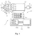
- Fig. 1 shows a schematic block diagram of an embodiment of the coherent receiver in accordance with the present invention.
- the coherent receiver 1 comprises an input 2 for inputting an optical signal OS and an output 3 for outputting a data signal DS based on said input optical signal OS.
- An optical hybrid 4 comprising a Polarisation Beam Splitter 5 is connected with said input 2 of coherent receiver 1.
- Optical hybrid 4 comprises four output ports 6.1-6.4 which are operatively connected with respective optical-to-electrical converting means 7.1-7.4 which may take the form of diodes. Furthermore, upstream of said output ports 6.1-6.4 respective signal paths within optical hybrid 4 are operatively connected with a local oscillator laser (LO) 8.
- LO local oscillator laser
- An electrical signal output of respective optical-to-electrical converting means 7.1-7.4 is provided to respective analog-to-digital converting means (ADCs) 9.1-9.4.
- ADCs 9.1-9.4 further receive a clock signal CS of the coherent receiver 1.
- the coherent receiver 1 in accordance with the present invention comprises digital signal processing (DSP) means 10, which are subdivided into first means 10.1 for fast digital signal processing, i.e., fast digital signal processing means, and second means 10.2 in the form of an adaptation control processor for controlling an operation of said first means 10.1.
- Second means 10.2 further comprise Fourier transformer 10.2a and numerical calculating means 10.2b.
- An output signal SI of DSP means 10 is provided to a decision unit 11 which provides said data signal DS to output 3 of the coherent receiver 1.
- Fig. 1 Operation of the coherent receiver 1 as depicted in Fig. 1 , which can be devised either as a homodyne or as a heterodyne receiver, they will now be described in some detail with reference to appended Fig. 1 .
- An optical signal OS input at 2 is split into two orthogonal polarisation states S, P. said polarisation states S, P of optical signal OS are further split up by performing vectorial additions with a reference signal RS provided by the LO 8.
- This standard operation of optical hybrid 4 is assumed to be known to a person skilled in the art.
- the resulting optical signals (not shown) are provided to output ports 6.1-6.4 of optical hybrid 4. They interact with optical-to-electrical converting means in the form of photo diodes 7.1-7.4, respectively, which produce electrical signals Is, Q S , I P , Q P associated with respective optical signals output from optical hybrid 4.
- optical hybrid 4 can also be referred to as "optical mixer" which, in conjunction with the respective photo diode 7.1-7.4, multiplies the received optical signal OS and the reference signal RS generates by LO 8 to provide said optical signals at output port 6.1-6.4 for generating said electrical signals I S , Q S , I P , Q P .
- the electrical signals I S , Q S , I P , Q P include real part electrical signals and imaginary part electrical signals, i.e., electrical signals I S , I P and electrical signals Q S , Q P , respectively.
- the signals provided at output port 6.1-6.4 of optical hybrid 4 are also referred to as beat frequency signals.
- the electrical signals Is, Q S , I P , Q P are provided to ADCs 9.1-9.4 for analog-to-digital conversion in synchronisation with clock signal CS.
- the digitised electrical signals provided to the DSP 10 from ADCs 9.1-9.4 contain the complete information of the optical field associated with received optical signal OS, including phase and polarisation information.
- First means 10.1 of DSP 10 then perform filtering of said digitised electrical signals essentially in real time in order to mitigate effects of polarisation distortion and provide a filtered signal as output signal SI to decision unit 11.
- Decision unit 11 decides on respective (binary) states of individual bits within output signal SI and outputs a result of said decision as data signal DS via output 3.
- blocks B1-B4 of signal samples of said digitised electrical signals corresponding to said electrical signals Is, Q S , I P , Q P are provided to adaptation control processor 10.2 from said first digital signal processing means 10.1.
- reference signs Is, Q S , I P , Q P have been used to designate both the electrical signals prior to analog-to-digital conversion by means of ADCs 9.1-9.4 and the resulting digitised electrical signals output from said ADCs 9.1-9.4.
- Each of said blocks B1-B4 comprises a number of N consecutive signal samples from respective digitised electrical signals Is, Q S , I P , and Q P , respectively.
- said blocks or sets B1-B4 of signal samples provided to second digital signal processing means 10.2 are delimited in bit number with respect to a number of bits comprised in the received optical signal.
- the number N of signal samples comprised in blocks B1-B4 is smaller than a number of bits N' (not shown) output by respective ADCs 9.1-9.4.
- first digital signal processing means 10.1 operate on the entire information provided by received optical signal OS
- the adaptation control processor or the second digital signal processing means 10.2 only operate on a limited set of information provided by received optical signal OS.
- first digital signal processing means 10.1 can also be referred to as fast digital signal processing means whereas the second digital signal processing means 10.2 can also be referred to as slow digital signal processing means.
- the first and second digital signal processing means 10.1 and 10.2 can either be implemented in form of the single chip architecture or can be comprised on separate chips.
- the adaptation control processor or second digital signal processing means 10.2 perform a Fourier transformation, in particular a Fast Fourier Transformation (FFT).
- FFT Fast Fourier Transformation
- the second digital signal processing means 10.2 are adapted to derive a number of polarisation spectra of the received optical signal.
- Fourier transformer 10.2a comprised within said second means 10.2 derives a first polarisation spectrum ("spectrum-S") from a signal I S +jQ S and a second polarisation spectrum (“spectrum-P”) from a signal I P +jQ P . Both of said signals are formed from the signal samples comprised within blocks B1-B4.
- Said spectra are then provided to numerical calculating means 10.2b which operate on the derived spectra to generate and/or adapt operation parameters of the first digital signal processing means 10.1 for optimising a performance characteristic of the latter.
- said performance characteristic can either be a minimum bit error ratio (BER) or a maximum eye opening or a maximum quality of signal (i.e., output signal SI), or other parameters derived from the processed signal samples and which are strongly correlated to an improved signal quality, as known to a person skilled in the art.
- said numerical calculating means 10.2b provide respective adaptation parameters or signal processor settings to said first digital signal processing means 10.1, said adaptation parameters being denoted C i,j , Ti, ...
- the polarisation spectra of a distorted (optical) input signal are used to determine optimum settings of the fast digital signal processing part 10.1 and thus to compensate the actual polarisation distortion by way of a feed-forward adaptation.
- the polarisation spectra are obtained by transferring a limited time span of consecutive signal samples (ranging, e.g., from 16 to 1024 or 2048 bits) to adaptation control processor 10.2, which can be located externally with respect to said fast digital signal processing means 10.1.
- Said adaptation control processor 10.2 numerically performs a discrete Fast Fourier Transformation (DFFT).
- DFFT discrete Fast Fourier Transformation
- said fast digital signal processing means 10.1 proposes numerical operations which follow the calculation rules of a lattice filter structure.
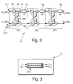
- said lattice filter structure as illustrated in Fig. 2 , may be comprised within the fast digital signal processing part 10.1 in Fig. 1 .
- Fig. 2 shows a schematic diagram of a lattice filter structure used within the receiver of Fig. 1 .
- the lattice filter structure 12 of Fig. 2 comprises two signal paths 12.1, 12.2 which receive complex input signals I1 S + jQ1 S and I1 P +jQ1 P , respectively.
- the lattice filter structure 12 comprises a number of stages ST1, ST2, ST3 each including respective multiplying means M1-M4, adding or combining means A1, A2 and delay means Di (D1, D2, D3). While said multiplying means M1-M4 and said adding means A1, A2 are identical for each of said stages ST1-ST3, said delay means D1-D3 may differ between stages with respect to their delay time ⁇ 1, ⁇ 2, ⁇ 3.
- Adding means A1, A2 serve to combine signal contributions on said first and second signal paths 12.1, 12.2 after respective multiplication by means of multiplying means M1, M2 and M3, M4, respectively.
- Multiplying means M1-M4 multiply an input signal with a coefficient C ij , which can be either real or complex valued. As can further be gathered from the illustration in Fig. 2 , said coefficients C ij form a 2 x 2 rotation matrix.
- the delay means D1-D3 are located in said first signal path 12.1 only and delay an input signal by a respective delay time ⁇ 1- ⁇ 3 downstream of adding or combining means A1.
- Respective output signals I2 S +jQ2 S , I2 P +jQ2 P on said first and second signal paths 12.1, 12.2, respectively are then used to form said output signal SI of digital signal processing means 10 ( Fig. 1 ).
- Delay means D1-D3 can have fixed or tuneable time delays ⁇ 1- ⁇ 3. According to an embodiment of the present invention, delay means D1-D3 are implemented in the form of shift registers, as depicted schematically in Fig. 3 .
- Fig. 3 shows a schematic diagram of a delay means used within the filter structure of Fig. 2 .
- a delay means generally denoted Di has a first input for a signal I i and a second input for the signal Q i .
- delay means Di has a first output for a signal I i-N at a second output for a signal Q i-N .
- Signal input and output of delay means Di is controlled in synchronisation with clock signal CS. In this way, if one bit of an input signal is input into the shift register a corresponding (older) bit is output from the shift register, as known to a person skilled in the art. In this way, for an N-bit shift register a bit i-N is output when inputting a bit i. In accordance with the value of N and a frequency of clock signal CS this amounts to a time delay ⁇ (N).
- the delay means Di; D1-D3 can also be implemented in the form of digital FIR filters.
- an alternative embodiment of the coherent receiver in accordance with the present invention may use a transversal filter (having a butterfly structure) for fast digital signal processing.
- a transversal filter having a butterfly structure
- any other DSP filter capable of filtering digitised electrical signals with high data rates in a reliable fashion to overcome polarisation distortion effects may be used for implementing the first digital signal processing means 10.1 of Fig. 1 .
- the signal samples comprised in blocks B1-B4 may be output from said first digital signal processing means 10.1 immediately downstream of ADCs 9.1-9.4. However, as will be appreciated by a person skilled in the art, optionally some signal (pre-)preprocessing may be performed prior to providing the signal samples of blocks B1-B4 from said first digital signal processing means 10.1 to said second digital signal processing means 10.2.
- the present invention achieves fast feed-forward adaptation for the mitigation of polarisation effects in a coherent receiver without the need for slow feedback (dithering).
Priority Applications (1)
| Application Number | Priority Date | Filing Date | Title |
|---|---|---|---|
| EP07290013A EP1942590A1 (fr) | 2007-01-03 | 2007-01-03 | Récepteur optique cohérent et procédé pour compensation de la distorsion liée à la polarisation des signaux dans un système de transmission à fibre optique |
Applications Claiming Priority (1)
| Application Number | Priority Date | Filing Date | Title |
|---|---|---|---|
| EP07290013A EP1942590A1 (fr) | 2007-01-03 | 2007-01-03 | Récepteur optique cohérent et procédé pour compensation de la distorsion liée à la polarisation des signaux dans un système de transmission à fibre optique |
Publications (1)
| Publication Number | Publication Date |
|---|---|
| EP1942590A1 true EP1942590A1 (fr) | 2008-07-09 |
Family
ID=38007342
Family Applications (1)
| Application Number | Title | Priority Date | Filing Date |
|---|---|---|---|
| EP07290013A Withdrawn EP1942590A1 (fr) | 2007-01-03 | 2007-01-03 | Récepteur optique cohérent et procédé pour compensation de la distorsion liée à la polarisation des signaux dans un système de transmission à fibre optique |
Country Status (1)
| Country | Link |
|---|---|
| EP (1) | EP1942590A1 (fr) |
Cited By (3)
| Publication number | Priority date | Publication date | Assignee | Title |
|---|---|---|---|---|
| EP2249493A1 (fr) * | 2009-05-05 | 2010-11-10 | Alcatel Lucent | Procédé et équipement pour faire fonctionner un récepteur de paquets optiques cohérent |
| EP2273701A1 (fr) * | 2009-06-30 | 2011-01-12 | Alcatel Lucent | Récepteur de détection cohérente en mode rafale optique doté d'un tampon et d'une partie de traitement de signaux supplémentaires pour déterminer les paramètres de réception initiaux |
| JP2011135176A (ja) * | 2009-12-22 | 2011-07-07 | Fujitsu Ltd | 光受信機および受信方法 |
Citations (7)
| Publication number | Priority date | Publication date | Assignee | Title |
|---|---|---|---|---|
| WO2003028267A1 (fr) * | 2001-09-26 | 2003-04-03 | Celight, Inc. | Attenuation de degradations de transmission non lineaire dans des systemes de communication par fibres optiques |
| WO2004054138A2 (fr) * | 2002-12-11 | 2004-06-24 | Taylor Michael G | Procede et systeme de detection optique coherente et de traitement du signal |
| US6782211B1 (en) * | 1998-11-05 | 2004-08-24 | Mark T. Core | Cross polarization interface canceler |
| US20050196176A1 (en) * | 2004-03-08 | 2005-09-08 | Han Sun | Equalization strategy for dual-polarization optical transport system |
| US20050286904A1 (en) * | 2002-09-17 | 2005-12-29 | Siemens Aktiengesellschaft | Method for the transmission of optical polarization multiplex signals |
| WO2007045070A1 (fr) * | 2005-10-21 | 2007-04-26 | Nortel Networks Limited | Transmission de donnees efficace et entrainement de fonctions de traitement des donnees |
| WO2007045071A1 (fr) * | 2005-10-21 | 2007-04-26 | Nortel Networks Limited | Recuperation d'horloge dans un signal optique reçu par un reseau de communication optique |
-
2007
- 2007-01-03 EP EP07290013A patent/EP1942590A1/fr not_active Withdrawn
Patent Citations (7)
| Publication number | Priority date | Publication date | Assignee | Title |
|---|---|---|---|---|
| US6782211B1 (en) * | 1998-11-05 | 2004-08-24 | Mark T. Core | Cross polarization interface canceler |
| WO2003028267A1 (fr) * | 2001-09-26 | 2003-04-03 | Celight, Inc. | Attenuation de degradations de transmission non lineaire dans des systemes de communication par fibres optiques |
| US20050286904A1 (en) * | 2002-09-17 | 2005-12-29 | Siemens Aktiengesellschaft | Method for the transmission of optical polarization multiplex signals |
| WO2004054138A2 (fr) * | 2002-12-11 | 2004-06-24 | Taylor Michael G | Procede et systeme de detection optique coherente et de traitement du signal |
| US20050196176A1 (en) * | 2004-03-08 | 2005-09-08 | Han Sun | Equalization strategy for dual-polarization optical transport system |
| WO2007045070A1 (fr) * | 2005-10-21 | 2007-04-26 | Nortel Networks Limited | Transmission de donnees efficace et entrainement de fonctions de traitement des donnees |
| WO2007045071A1 (fr) * | 2005-10-21 | 2007-04-26 | Nortel Networks Limited | Recuperation d'horloge dans un signal optique reçu par un reseau de communication optique |
Non-Patent Citations (1)
| Title |
|---|
| CRIVELLI D E ET AL: "Adaptive digital equalization in the presence of chromatic dispersion, PMD, and phase noise in coherent fiber optic systems", GLOBAL TELECOMMUNICATIONS CONFERENCE, 2004. GLOBECOM '04. IEEE DALLAS, TX, USA 29 NOV.-3 DEC., 2004, PISCATAWAY, NJ, USA,IEEE, vol. 4, 29 November 2004 (2004-11-29), pages 2545 - 2551, XP010757986, ISBN: 0-7803-8794-5 * |
Cited By (7)
| Publication number | Priority date | Publication date | Assignee | Title |
|---|---|---|---|---|
| EP2249493A1 (fr) * | 2009-05-05 | 2010-11-10 | Alcatel Lucent | Procédé et équipement pour faire fonctionner un récepteur de paquets optiques cohérent |
| WO2010127886A1 (fr) * | 2009-05-05 | 2010-11-11 | Alcatel Lucent | Procédé et équipement permettant de faire fonctionner un récepteur de paquet optique cohérent |
| CN102422572A (zh) * | 2009-05-05 | 2012-04-18 | 阿尔卡特朗讯 | 用于操作相干光学分组接收机的方法和设备 |
| US9178612B2 (en) | 2009-05-05 | 2015-11-03 | Alcatel Lucent | Method and equipment for operating a coherent optical packet receiver |
| CN102422572B (zh) * | 2009-05-05 | 2016-01-20 | 阿尔卡特朗讯 | 用于操作相干光学分组接收机的方法和设备 |
| EP2273701A1 (fr) * | 2009-06-30 | 2011-01-12 | Alcatel Lucent | Récepteur de détection cohérente en mode rafale optique doté d'un tampon et d'une partie de traitement de signaux supplémentaires pour déterminer les paramètres de réception initiaux |
| JP2011135176A (ja) * | 2009-12-22 | 2011-07-07 | Fujitsu Ltd | 光受信機および受信方法 |
Similar Documents
| Publication | Publication Date | Title |
|---|---|---|
| US8275267B2 (en) | Method, system, and apparatus for filter implementation using hermitian conjugates | |
| US8477056B2 (en) | Method, system, and apparatus for interpolating an output of an analog-to-digital converter | |
| EP1949569B1 (fr) | Compensation de polarisation dans un recepteur optique coherent | |
| JP6405833B2 (ja) | 信号処理装置及び信号処理方法 | |
| US9014574B2 (en) | Optical receiver, polarization demultiplexer, and optical receiving method | |
| EP2034637B1 (fr) | Contrôleur de conversion analogique-numérique, dispositif de réception optique, procédé de réception optique, et dispositif de compensation de distorsion à forme d'ondes | |
| US8260153B2 (en) | Method and apparatus for polarization-division-multiplexed optical coherent receivers | |
| US8831081B2 (en) | Digital filter device, digital filtering method and control program for the digital filter device | |
| JP6458733B2 (ja) | 光受信装置、光伝送システムおよび光受信方法 | |
| US8903255B2 (en) | Polarization-multiplexed signal receiver, polarization multiplexing system and polarization-multiplexed signal receiving method | |
| US10998973B2 (en) | Signal combining device and signal combining method | |
| JP2010050578A (ja) | 歪補償器、光受信装置およびそれらの制御方法並びに光伝送システム | |
| EP2465219B1 (fr) | Dispositif de filtrage | |
| US6856724B2 (en) | Compensation system for adaptive equalization of an optical signal | |
| EP1942590A1 (fr) | Récepteur optique cohérent et procédé pour compensation de la distorsion liée à la polarisation des signaux dans un système de transmission à fibre optique | |
| JP2014050056A (ja) | 信号処理装置及び信号処理方法 | |
| CN115412175A (zh) | 一种光均衡设备、接收设备以及通信系统 | |
| JP6219861B2 (ja) | 空間多重光伝送システム及び空間多重光伝送方法 | |
| JP5338593B2 (ja) | 分散等化回路および光トランシーバ | |
| JP4758172B2 (ja) | 色および/または分極化モード分散補償用適応光学等化、および結合光電子等化装置構造 | |
| JP2005006151A (ja) | 非線形フィルタ回路 | |
| US20230170994A1 (en) | Adaptive equalizer, equalization method, and optical communication system | |
| JPH08163027A (ja) | 光信号受信処理回路 | |
| US20060045538A1 (en) | Device and a method for processing a digital signal in a bit-to-bit polarization-interleaved format of an optical transmission system | |
| EP3133751A1 (fr) | Procédé de compensation de non-linéarité dans des systèmes de transmission optique |
Legal Events
| Date | Code | Title | Description |
|---|---|---|---|
| PUAI | Public reference made under article 153(3) epc to a published international application that has entered the european phase |
Free format text: ORIGINAL CODE: 0009012 |
|
| AK | Designated contracting states |
Kind code of ref document: A1 Designated state(s): AT BE BG CH CY CZ DE DK EE ES FI FR GB GR HU IE IS IT LI LT LU LV MC NL PL PT RO SE SI SK TR |
|
| AX | Request for extension of the european patent |
Extension state: AL BA HR MK RS |
|
| 17P | Request for examination filed |
Effective date: 20080910 |
|
| AKX | Designation fees paid |
Designated state(s): AT BE BG CH CY CZ DE DK EE ES FI FR GB GR HU IE IS IT LI LT LU LV MC NL PL PT RO SE SI SK TR |
|
| 17Q | First examination report despatched |
Effective date: 20100422 |
|
| RAP1 | Party data changed (applicant data changed or rights of an application transferred) |
Owner name: ALCATEL LUCENT |
|
| 111Z | Information provided on other rights and legal means of execution |
Free format text: AT BE BG CH CY CZ DE DK EE ES FI FR GB GR HU IE IS IT LI LT LU LV MC NL PL PT RO SE SI SK TR Effective date: 20130410 |
|
| RAP1 | Party data changed (applicant data changed or rights of an application transferred) |
Owner name: ALCATEL LUCENT |
|
| D11X | Information provided on other rights and legal means of execution (deleted) | ||
| GRAP | Despatch of communication of intention to grant a patent |
Free format text: ORIGINAL CODE: EPIDOSNIGR1 |
|
| RIC1 | Information provided on ipc code assigned before grant |
Ipc: H04B 10/61 20130101AFI20160208BHEP |
|
| INTG | Intention to grant announced |
Effective date: 20160226 |
|
| STAA | Information on the status of an ep patent application or granted ep patent |
Free format text: STATUS: THE APPLICATION IS DEEMED TO BE WITHDRAWN |
|
| 18D | Application deemed to be withdrawn |
Effective date: 20160708 |