EP1540779B1 - Schnelle, dichte verbindungseinrichtung - Google Patents
Schnelle, dichte verbindungseinrichtung Download PDFInfo
- Publication number
- EP1540779B1 EP1540779B1 EP03761284A EP03761284A EP1540779B1 EP 1540779 B1 EP1540779 B1 EP 1540779B1 EP 03761284 A EP03761284 A EP 03761284A EP 03761284 A EP03761284 A EP 03761284A EP 1540779 B1 EP1540779 B1 EP 1540779B1
- Authority
- EP
- European Patent Office
- Prior art keywords
- contacts
- contact
- segment
- signal
- intercoupling component
- Prior art date
- Legal status (The legal status is an assumption and is not a legal conclusion. Google has not performed a legal analysis and makes no representation as to the accuracy of the status listed.)
- Expired - Lifetime
Links
- 230000005540 biological transmission Effects 0.000 claims abstract description 34
- 239000004020 conductor Substances 0.000 claims abstract description 27
- 239000000463 material Substances 0.000 claims abstract description 22
- 238000004891 communication Methods 0.000 claims description 9
- 239000003989 dielectric material Substances 0.000 claims description 4
- 230000014759 maintenance of location Effects 0.000 claims description 2
- 229910000679 solder Inorganic materials 0.000 description 15
- 230000005672 electromagnetic field Effects 0.000 description 11
- 238000000034 method Methods 0.000 description 9
- 230000011664 signaling Effects 0.000 description 7
- 239000002131 composite material Substances 0.000 description 6
- 230000013011 mating Effects 0.000 description 6
- 238000005476 soldering Methods 0.000 description 6
- 230000000694 effects Effects 0.000 description 5
- 230000008569 process Effects 0.000 description 5
- 230000008054 signal transmission Effects 0.000 description 5
- 239000011347 resin Substances 0.000 description 4
- 229920005989 resin Polymers 0.000 description 4
- 239000004734 Polyphenylene sulfide Substances 0.000 description 3
- 238000013459 approach Methods 0.000 description 3
- 229920000069 polyphenylene sulfide Polymers 0.000 description 3
- 230000001902 propagating effect Effects 0.000 description 3
- 229920006362 Teflon® Polymers 0.000 description 2
- 238000003491 array Methods 0.000 description 2
- 238000004364 calculation method Methods 0.000 description 2
- 230000015556 catabolic process Effects 0.000 description 2
- 238000005094 computer simulation Methods 0.000 description 2
- 238000010276 construction Methods 0.000 description 2
- 238000006731 degradation reaction Methods 0.000 description 2
- 238000001746 injection moulding Methods 0.000 description 2
- 238000002955 isolation Methods 0.000 description 2
- 230000003071 parasitic effect Effects 0.000 description 2
- 238000012545 processing Methods 0.000 description 2
- 230000009467 reduction Effects 0.000 description 2
- 229910000881 Cu alloy Inorganic materials 0.000 description 1
- 239000000853 adhesive Substances 0.000 description 1
- 230000001070 adhesive effect Effects 0.000 description 1
- 230000002411 adverse Effects 0.000 description 1
- 230000000740 bleeding effect Effects 0.000 description 1
- 239000004568 cement Substances 0.000 description 1
- 230000008878 coupling Effects 0.000 description 1
- 238000010168 coupling process Methods 0.000 description 1
- 238000005859 coupling reaction Methods 0.000 description 1
- 230000001419 dependent effect Effects 0.000 description 1
- 238000013461 design Methods 0.000 description 1
- 238000005516 engineering process Methods 0.000 description 1
- 230000006870 function Effects 0.000 description 1
- 239000011521 glass Substances 0.000 description 1
- 239000003292 glue Substances 0.000 description 1
- 238000003475 lamination Methods 0.000 description 1
- 239000002184 metal Substances 0.000 description 1
- 229910052751 metal Inorganic materials 0.000 description 1
- 238000012986 modification Methods 0.000 description 1
- 230000004048 modification Effects 0.000 description 1
- 230000000717 retained effect Effects 0.000 description 1
Images


Classifications
-
- H—ELECTRICITY
- H01—ELECTRIC ELEMENTS
- H01R—ELECTRICALLY-CONDUCTIVE CONNECTIONS; STRUCTURAL ASSOCIATIONS OF A PLURALITY OF MUTUALLY-INSULATED ELECTRICAL CONNECTING ELEMENTS; COUPLING DEVICES; CURRENT COLLECTORS
- H01R12/00—Structural associations of a plurality of mutually-insulated electrical connecting elements, specially adapted for printed circuits, e.g. printed circuit boards [PCB], flat or ribbon cables, or like generally planar structures, e.g. terminal strips, terminal blocks; Coupling devices specially adapted for printed circuits, flat or ribbon cables, or like generally planar structures; Terminals specially adapted for contact with, or insertion into, printed circuits, flat or ribbon cables, or like generally planar structures
- H01R12/70—Coupling devices
- H01R12/71—Coupling devices for rigid printing circuits or like structures
- H01R12/712—Coupling devices for rigid printing circuits or like structures co-operating with the surface of the printed circuit or with a coupling device exclusively provided on the surface of the printed circuit
- H01R12/716—Coupling device provided on the PCB
-
- H—ELECTRICITY
- H01—ELECTRIC ELEMENTS
- H01R—ELECTRICALLY-CONDUCTIVE CONNECTIONS; STRUCTURAL ASSOCIATIONS OF A PLURALITY OF MUTUALLY-INSULATED ELECTRICAL CONNECTING ELEMENTS; COUPLING DEVICES; CURRENT COLLECTORS
- H01R13/00—Details of coupling devices of the kinds covered by groups H01R12/70 or H01R24/00 - H01R33/00
- H01R13/02—Contact members
- H01R13/15—Pins, blades or sockets having separate spring member for producing or increasing contact pressure
- H01R13/187—Pins, blades or sockets having separate spring member for producing or increasing contact pressure with spring member in the socket
-
- H—ELECTRICITY
- H01—ELECTRIC ELEMENTS
- H01R—ELECTRICALLY-CONDUCTIVE CONNECTIONS; STRUCTURAL ASSOCIATIONS OF A PLURALITY OF MUTUALLY-INSULATED ELECTRICAL CONNECTING ELEMENTS; COUPLING DEVICES; CURRENT COLLECTORS
- H01R13/00—Details of coupling devices of the kinds covered by groups H01R12/70 or H01R24/00 - H01R33/00
- H01R13/40—Securing contact members in or to a base or case; Insulating of contact members
- H01R13/405—Securing in non-demountable manner, e.g. moulding, riveting
-
- H—ELECTRICITY
- H01—ELECTRIC ELEMENTS
- H01R—ELECTRICALLY-CONDUCTIVE CONNECTIONS; STRUCTURAL ASSOCIATIONS OF A PLURALITY OF MUTUALLY-INSULATED ELECTRICAL CONNECTING ELEMENTS; COUPLING DEVICES; CURRENT COLLECTORS
- H01R13/00—Details of coupling devices of the kinds covered by groups H01R12/70 or H01R24/00 - H01R33/00
- H01R13/46—Bases; Cases
- H01R13/514—Bases; Cases composed as a modular blocks or assembly, i.e. composed of co-operating parts provided with contact members or holding contact members between them
-
- H—ELECTRICITY
- H01—ELECTRIC ELEMENTS
- H01R—ELECTRICALLY-CONDUCTIVE CONNECTIONS; STRUCTURAL ASSOCIATIONS OF A PLURALITY OF MUTUALLY-INSULATED ELECTRICAL CONNECTING ELEMENTS; COUPLING DEVICES; CURRENT COLLECTORS
- H01R13/00—Details of coupling devices of the kinds covered by groups H01R12/70 or H01R24/00 - H01R33/00
- H01R13/646—Details of coupling devices of the kinds covered by groups H01R12/70 or H01R24/00 - H01R33/00 specially adapted for high-frequency, e.g. structures providing an impedance match or phase match
- H01R13/6461—Means for preventing cross-talk
- H01R13/6471—Means for preventing cross-talk by special arrangement of ground and signal conductors, e.g. GSGS [Ground-Signal-Ground-Signal]
-
- H—ELECTRICITY
- H01—ELECTRIC ELEMENTS
- H01R—ELECTRICALLY-CONDUCTIVE CONNECTIONS; STRUCTURAL ASSOCIATIONS OF A PLURALITY OF MUTUALLY-INSULATED ELECTRICAL CONNECTING ELEMENTS; COUPLING DEVICES; CURRENT COLLECTORS
- H01R13/00—Details of coupling devices of the kinds covered by groups H01R12/70 or H01R24/00 - H01R33/00
- H01R13/646—Details of coupling devices of the kinds covered by groups H01R12/70 or H01R24/00 - H01R33/00 specially adapted for high-frequency, e.g. structures providing an impedance match or phase match
- H01R13/6473—Impedance matching
- H01R13/6477—Impedance matching by variation of dielectric properties
-
- H—ELECTRICITY
- H01—ELECTRIC ELEMENTS
- H01R—ELECTRICALLY-CONDUCTIVE CONNECTIONS; STRUCTURAL ASSOCIATIONS OF A PLURALITY OF MUTUALLY-INSULATED ELECTRICAL CONNECTING ELEMENTS; COUPLING DEVICES; CURRENT COLLECTORS
- H01R13/00—Details of coupling devices of the kinds covered by groups H01R12/70 or H01R24/00 - H01R33/00
- H01R13/648—Protective earth or shield arrangements on coupling devices, e.g. anti-static shielding
- H01R13/658—High frequency shielding arrangements, e.g. against EMI [Electro-Magnetic Interference] or EMP [Electro-Magnetic Pulse]
- H01R13/6581—Shield structure
- H01R13/6585—Shielding material individually surrounding or interposed between mutually spaced contacts
- H01R13/6586—Shielding material individually surrounding or interposed between mutually spaced contacts for separating multiple connector modules
-
- H—ELECTRICITY
- H01—ELECTRIC ELEMENTS
- H01R—ELECTRICALLY-CONDUCTIVE CONNECTIONS; STRUCTURAL ASSOCIATIONS OF A PLURALITY OF MUTUALLY-INSULATED ELECTRICAL CONNECTING ELEMENTS; COUPLING DEVICES; CURRENT COLLECTORS
- H01R13/00—Details of coupling devices of the kinds covered by groups H01R12/70 or H01R24/00 - H01R33/00
- H01R13/648—Protective earth or shield arrangements on coupling devices, e.g. anti-static shielding
- H01R13/658—High frequency shielding arrangements, e.g. against EMI [Electro-Magnetic Interference] or EMP [Electro-Magnetic Pulse]
- H01R13/6591—Specific features or arrangements of connection of shield to conductive members
-
- H—ELECTRICITY
- H01—ELECTRIC ELEMENTS
- H01R—ELECTRICALLY-CONDUCTIVE CONNECTIONS; STRUCTURAL ASSOCIATIONS OF A PLURALITY OF MUTUALLY-INSULATED ELECTRICAL CONNECTING ELEMENTS; COUPLING DEVICES; CURRENT COLLECTORS
- H01R13/00—Details of coupling devices of the kinds covered by groups H01R12/70 or H01R24/00 - H01R33/00
- H01R13/648—Protective earth or shield arrangements on coupling devices, e.g. anti-static shielding
- H01R13/658—High frequency shielding arrangements, e.g. against EMI [Electro-Magnetic Interference] or EMP [Electro-Magnetic Pulse]
- H01R13/6598—Shield material
-
- H—ELECTRICITY
- H01—ELECTRIC ELEMENTS
- H01R—ELECTRICALLY-CONDUCTIVE CONNECTIONS; STRUCTURAL ASSOCIATIONS OF A PLURALITY OF MUTUALLY-INSULATED ELECTRICAL CONNECTING ELEMENTS; COUPLING DEVICES; CURRENT COLLECTORS
- H01R12/00—Structural associations of a plurality of mutually-insulated electrical connecting elements, specially adapted for printed circuits, e.g. printed circuit boards [PCB], flat or ribbon cables, or like generally planar structures, e.g. terminal strips, terminal blocks; Coupling devices specially adapted for printed circuits, flat or ribbon cables, or like generally planar structures; Terminals specially adapted for contact with, or insertion into, printed circuits, flat or ribbon cables, or like generally planar structures
- H01R12/50—Fixed connections
- H01R12/51—Fixed connections for rigid printed circuits or like structures
- H01R12/52—Fixed connections for rigid printed circuits or like structures connecting to other rigid printed circuits or like structures
Definitions
- This description relates to intercoupling components and a method for adjusting the differential impedance of a pair of differential transmission lines in an interconnection device, and more particularly to interconnection devices which connect an array of contacts within a digital or analog transmission system.
- Each connector includes a conductive housing having a cavity for receiving at least two signal terminals and at least one ground terminal.
- US patent US6371773, dated April 16, 2002, inventors Crofoot et al , assignee Ohio Associated Enterprises Inc. relates to an electrical interconnect system that allows high signal density with means of electrical isolation to minimize degradation of electrical signals.
- an intercoupling component according to appended claim 1.
- a circuit card according to appended claim 32.
- An embodiment features an intercoupling component for receiving an array of contacts within a digital or analog transmission system having an electrical ground circuit and a chassis ground circuit.
- a plurality of electrically conductive contacts are disposed within holes formed on a segment formed of insulative material.
- One or more electrically conductive shields are disposed within the segment and are configured to connect to the chassis ground circuit of the system.
- Embodiments may include one or more of the following. At least some of the plurality of the electrically conductive contacts disposed within the holes on the segment may be configured to electrically connect with the electrical ground circuit of the system.
- a frame formed of electrically conductive material may surround the segment and be in electrical contact with both the shield member and the electrical ground circuit of the system.
- the frame may be molded around the segments.
- One or more ground planes which are configured to electrically connect with the electrical ground circuit of the system may be disposed within the segment.
- One or more cavities filled with air may be disposed on the segment.
- the intercoupling component may further include a retention member configured to releasably retain an array mating of contacts with the plurality of electrically conductive contacts,
- Another embodiment features an intercoupling component for receiving an array of contacts within a digital or analog transmission system having an electrical ground circuit and a chassis ground circuit.
- a plurality of electrically conductive contacts are disposed within holes formed on a plurality of segments, each formed of insulative material.
- One or more electrically conductive shields are disposed within gaps between adjacent segments and are connected to the chassis ground circuit of the system.
- Another embodiment features an intercoupling component for receiving an array of contacts within a digital or analog transmission system having one or more segments formed of electrically insulative material and having an upper and lower surface the segment including a plurality of holes disposed on its upper surface and arranged in a predetermined footprint corresponding to the array of a contacts and a plurality of electrically conductive contacts each disposed within each hole on the upper surface of the segment.
- the plurality of contacts are arranged in a plurality of multi- contact groupings, with at least one multi-contact grouping including a first signal contact and a reference contact
- the reference contact is located at a first distance from the first signal contact and is configured to electrically connect to the electrical ground circuit of the system.
- Embodiments may include one or more of the following.
- the first signal contact and reference contact may be configured to form a transmission line electrically equivalent to a co-axial transmission line.
- the first signal contact may be configured to transmit single-ended signals.
- each multi- contact grouping may be located a distance of > the first distance from adjacent multi-contact groupings.
- the intercoupling component may also include a second electrically conductive contact member located at a second distance from the first electrically conductive contact.
- the first and second signal contacts may form a transmission line electrically equivalent to a twin-axial differential transmission line.
- the first and second signal contacts within each multi-contact grouping may be configured to transmit disparate single-ended signals or low-voltage differential signals. Additionally, each multi-contact grouping may be located a distance > D2 from adjacent multi-contact groupings.
- the first and second signal contacts may have substantially the same cross-section, initial characteristic impedance, capacitance, and inductance.
- the intercoupling component may also include one or more shield members formed of electrically conductive material disposed within the segment and configured to connect to the chassis ground circuit of the system. Additionally, the intercoupling component may include a frame disposed around the one or more segments.
- circuit card for use in a digital or analog transmission system having an electrical ground circuit and a chassis ground circuit
- the circuit card includes a printed circuit board having a plurality of contact pads arranged in a predetermined footprint; and an interconnection device.
- the interconnection device includes one or more segments having an upper and lower surface, the upper surface of the segment having a plurality of holes arranged in a predetermined footprint to match the predetermined footprint of the plurality of surface mount pads, a plurality of electrically conductive contact member disposed within each of the holes and electrically connected to their respective surface mount pad, and one or more a shield members formed of electrically conductive material disposed within the segment.
- a frame formed of electrically conductive material surrounds the one or more segments and the frame is electrically connected the shield member and to the chassis ground circuit of the system.
- the plurality of contacts may be arranged in a plurality of multi-contact groupings which includes a first signal contact; and a reference contact located at a first distance from the first signal contact and connected to the electrical ground circuit of the system.
- the plurality of multi-contact groupings may also include a second signal contact located a second distance from the first signal contact.
- the first and second signal contacts have substantially the same cross-section, capacitance and inductance.
- the first and second electrically conductive contacts may be configured to transmit low voltage differential signals or disparate single ended signals.
- an intercoupling component for receiving an array of contacts within a digital or analog transmission system having an electrical ground circuit
- the intercoupling component includes a segment formed of a material having a dielectric constant Erl.
- the segment has an upper and lower surface and a plurality of holes are disposed on the upper surface of the segment.
- a first signal contact disposed within a first hole on the segment and a second signal contact disposed within a second hole on the segment adjacent to the first hole in which the first signal contact is disposed.
- the segment also includes a cavity formed between the first and second signal contacts.
- the cavity may be formed on the upper surface, lower surface or within the segment and may be is open to air.
- An insert formed of a material having a dielectric constant of Er 2 may be disposed within the cavity.
- the intercoupling component may include a plurality of first signal contacts disposed within a plurality of holes and a plurality of second signal contacts each disposed within a hole that is adjacent to a hole containing a first signal contact.
- the segment may include a cavity disposed between each pair of first and second signal contacts.
- the intercoupling component may also include ground contacts disposed within holes on the segment or a ground plane.
- Additional embodiments include one or more of the following steps. Inserting a material having a dielectric constant of Er 2 in the cavity in the segment.
- the plurality of ground contacts electrically connected to the electrical ground circuit of the system.
- ground plane disposed within the segment and within the array of pairs of signal contacts, the ground plane configured to electrically connect with the electrical ground of the system.
- Embodiments of the invention may have one or more of the following advantages.
- One or more contacts disposed within the array of contacts and are configured to connect to the electrical ground of the system may help to reduce cross-talk between two or more contacts during signal transmission. Additionally, the use of a electrically conductive shield member connected to the chassis ground of the system and disposed within or between one or more segments may help to reduce undesired electromagnetic fields generated by high-speed electron flow over the contact array during operation.
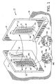
- a plug 12 and matching socket 14 releasably connect two printed circuit boards, a primary circuit board 18 and a secondary circuit board 16.
- Digital or analog transmission system 10 may be any system which transmits digital or analog signals over one or more transmission lines, such as a computer system (as illustrated in FIG 1 ), a telephony switch, a multiplexor/demultiplexor (MUX/DMUX), or a LAN/WAN cross-connect/router.
- a computer system as illustrated in FIG 1
- MUX/DMUX multiplexor/demultiplexor
- LAN/WAN cross-connect/router LAN/WAN cross-connect/router
- Secondary circuit board 16 may include a central processing unit (CPU), application specific integrated circuit (ASIC), memory, or similar active or passive devices and components.
- secondary circuit board 16 includes anASIC device 24, and primary circuit board 18 is a daughter board connected to a motherboard 20 by a card slot connector 22.
- the primary circuit board may be a self-contained system or board, not connecting to any other system or motherboard, as in the case of a single board computer.
- the socket 14 includes a frame 30 formed of electrically conductive material that surrounds a number of segments 32.
- the segments 32 are formed of electrically insulative material.
- a shield (not shown in FIG. 1 ) formed of electrically conductive material is located between each of the segments 32 and is in electrical contact with the frame 30, thus forming an electrically conductive"cage"around the perimeter of each segment 32.
- the frame 30 is electrically connected to the chassis ground circuit (shown in FIG 6 ) of the system 10.
- the socket 14 has an array of holes arranged in a series of three-hole groupings 35 on each segment 32.
- a female socket assembly 34 (not shown in FIG. 1 ) is located within each of the holes 33a-33c and is configured to releasably receive a male pin.
- the three-contact grouping 35 includes a first signal contact (disposed within hole 33a), a second signal contact (disposed within hole 33b) and a reference contact (disposed within hole 33c).
- the reference contact is electrically connected to the electrical ground circuit (Vcc) (shown in FIG 6 ) of the system 10.
- Plug 12 which mates with socket 14, also includes a frame 40 formed of electrically conductive material that surrounds a number of segments 42. Like the socket segments 32, the plug segments 42 are formed of electrically insulative material. A shield (not shown in FIG 1 ) formed of electrically conductive material is located between each of the segments 42 and is in electrical contact with the frame 40, thus forming an electrically conductive "cage" around the perimeter of each segment 42 within the plug 12. As will be explained more below, the frame 40 is electrically connected to the chassis ground circuit (shown in FIG 6 ) of the system 10.
- the plug 12 has an array of male pins 44 arranged in a series of three-pin groupings 45 on each segment 42.
- Each three-pin grouping 45 includes a first signal pin 44a, a second signal pin 44b and a reference pin 44c. As will be explained in greater detail below, these three pins mate with their respective sockets to form a twin-axial communication channel and a reference ground return between the plug 12 and socket 14.
- Each of the male pins 44 protrude from the upper surface of the segments 42 and are received by the matching array of female sockets (not shown) disposed within each of the holes 34 on the socket 14.
- Each male pin and female socket attach to a solder ball (not shown in FIG 1 ) that protrudes from the bottom surface of the plug 12 and socket 14, respectively, and is mounted via a solder reflow process to contact pads on the respective printed circuit boards, 16, 18.
- the male pins 44 and female sockets 34 may not be terminated by a solder reflow process using solder balls, but may employ other methods for mounting the pins or sockets to a printed circuit card, such as through-hole soldering, surface mount soldering, through-hole compliant pin, or surface pad pressure mounting.
- the plug frame 40 includes three guide notches 46a, 46b, 46c which mate with the three guide tabs 36a, 36b, 36c on the socket frame 30 in order to ensure proper orientation of the plug 12 and the socket 14 when mated together.
- each male pin 44 extends from the lower surface of the plug 12 and protrudes from the upper surface of the segments 42.
- a solder ball 50 is attached (e.g., by soldering) to the terminal end of each male pin 44 and protrudes from the bottom surface of the plug.
- the array of solder balls 50 attached to the terminal end of each male pin 44 may be mounted (e.g., by a solder reflow process) to contact pads located on the secondary circuit board 16.
- the plug frame 40 is formed of electrically conductive material and includes solder balls 52 are attached (e.g., by a solder reflow process) to the bottom surface of the plug frame 40.
- solder balls 52 are attached (e.g., by a solder reflow process) to the bottom surface of the plug frame 40.
- the solder balls 52 attached to the plug frame 40 are electrically connected to the chassis ground circuit of the system 10.
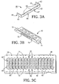
- FIGS. 3A-C a shield ( FIG. 3A ), a segment ( FIG 3B ) and the bottom surface of the plug ( FIG 3C ) is shown.
- a shield 60 formed of electrically conductive material is located between each of the segments 42.
- Each shield 60 is generally U-shaped and includes two short sides 61, 62 on each side of a longer middle portion 63. When assembled into the plug, the two short sides 61, 62 of each shield 60 are in electrical contact with the frame 40, while the middle portion 63 of each shield 60 is located between each of the segments 42.
- the frame 40 and shields 60 form a electrically conductive "cage" around the perimeter of each segment 42.
- This electrically conductive “cage” is connected to the chassis ground circuit (shown in FIG 6 ) of the system 10 via solder balls 52 on the bottom of the frame 40.
- the chassis ground circuit is a circuit within system 10 which connects to the metal structure on or in which the components of the system are mounted.
- each shield 60 has four notches: two on the short sides of the shield 64, 65 and two on the middle portion of the shield 66, 67.
- the two notches on the short sides of each shield 64, 65 mate with the two dog-eared tabs 71, 72 on each corresponding segment 42.
- the two notches located on the middle portion 66, 67 of each shield 60 mate with two corresponding tabs (not shown) on each segment 42.
- Each shield 60 also has three tabs 68 on it's middle portion 63 which are pressed in opposite directions by adjacent segments 42 after the plug 12 assembled and helps to secure the shields 60 in place.
- Each segment 42 includes two dog-eared tabs 71, 72 located at each end of the segment 42.
- the two dog-eared tabs 71, 72 fit into two matching grooves 81, 82 formed on the bottom surface of the frame 40.
- the two triangular bump-outs 73, 74 on each of the segments 42 press against adjacent shields 60 and segments 42 in order to secure the segments 42 and the shields 60 within the frame 40.
- the frame 40 may also be constructed by partially encapsulating the segments 42 with an electrically conductive resin or other material.
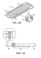
- the socket 14 has an array of holes (e.g., 33a, 33b, 33c) disposed on the segments 32.
- a female socket contact 34 is disposed within each of the holes and is configured to releasably receive a corresponding male pin 44.
- a solder ball contact 90 is attached (e.g., by soldering) to the terminal end of each female socket contact 34 and protrudes from the bottom surface of the socket 12.
- the array of solder balls 90 attached to the terminal end of each female socket contact 34 may be mounted (e.g., by soldering) to contact pads located on the primary circuit board 18.
- the socket frame 30 is formed of electrically conductive material and includes solder balls 92 attached (e.g., by soldering) to the bottom surface of the socket frame 30.
- solder balls 92 attached to the socket frame 30 are electrically connected to contact pads which are connected to the chassis ground circuit of the system 10.
- the plug frame 40 and socket frame 30 are electrically connected to each other and are, in turn, electrically connected to the chassis ground circuit of the system 10.
- the assembly of the socket 14 is similar to the assembly of the plug 12 depicted in FIGS. 3A-C .
- Dog-eared tabs 102, 103 located on the socket segments 32 fit into corresponding notches 104, 105 disposed on the socket frame 30.
- a shield 100 is located between each of the segments and electrically contacts the socket frame 30, thus forming an electrically conductive "cage" around the perimeter of each socket segment 32.
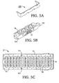
- the male pins 44 on the plug 12 and corresponding female socket contacts 34 disposed within the socket 14 may be any mating pair of interconnection contacts and not restricted to pin-and-socket technology.
- other embodiments may use fork and blade, beam-on-beam, beam-on-pad, or pad-on-pad interconnection contacts.
- the choice of contact may effect the differential impedance of the signal channels.
- differential signal communication over a single three-contact grouping between secondary circuit board 16 and primary circuit board 18 is illustrated.
- the plug 12 mounted to the secondary circuit board 16 is plugged into the socket 14 mounted to the primary circuit board 18, forming an electrical connection between the primary and secondary circuit boards, 16, 18.
- three male pins (not shown in FIG 6 ) of the plug 12 and three corresponding female socket contacts of socket 14 couple to form a first signal channel 108, a second signal channel 110, and a reference channel 112.
- the first and second signal channels 108, 110 are coupled with a resistor 118 to form a symmetric differential pair transmission line.
- the reference channel 112 is electrically connected to the electrical ground circuit (Vcc) 114 of the system 10.
- the electrical ground circuit (Vcc) 114 is a circuit within system 10 that is electrically connected to the power supply (not shown) of system 10 and provides the reference ground for system 10. Additionally, the plug frame 40 and socket frame 50 are in electrical contact with each another and with the chassis ground circuit 120 of the system 10.
- an ASIC chip 24 mounted to the secondary circuit board 18 includes a driver 100a which sends signals over the first and second signal channels, 108, 110.
- the primary circuit board 18 includes a receiver 116 which receives the signals generated by the driver 100a.
- the receiver 116 may be incorporated within a memory device, a central processing unit (CPU), an ASIC, or another active or passive device.
- the receiver 116 includes a resistor 118 between the first signal channel 108 and the second signal channel 110. In order to avoid signal reflection due to mismatched impedance, the differential impedance of the first and second signal channels, 108, 110 should be such that it approximately matches the value of the resistor 118.
- the driver 100a includes a current source 102a and four driver gates 104a-104b, 106a-106b and drives the differential pair line (i.e., first and second signal channels 108, 110).
- the receiver 116 has a high DC input impedance, so the majority of driver 100a current flows across the resistor 118, generating a voltage across the receiver 116 inputs.
- driver gates 106a-106b are closed (i.e., able to conduct current) and driver gates 104a-104b are open (i.e., not able to conduct current)
- a positive voltage is generated across the receiver 116 inputs which may be associated with a valid "one" logic state.
- the driver switches and driver gates 104a-104b are closed and driver gates 106a-106b are open, a negative voltage is generated across the receiver inputs which may be associated with a valid "zero" logic state.
- differential signaling creates two balanced signals propagating in opposite directions over the first and second signal channels, 108, 110.
- the electromagnetic field generated by current flow of the signal propagating over the first signal channel 108 is partially cancelled by the electromagnetic field generated by the current flow of the signal propagating over the second signal channel 110 once the differential signals become co-incidental or "in-line" with one another.
- the differential signaling reduces cross-talk between the first and second signal channels and between adjacent contact groupings.
- the addition of the reference channel 112 in close proximity to the first and second channels 108, 110 functions to help bleed off the parasitic electromagnetic field to circuit ground 114, which may further reduce cross-talk between signal channels and between contact groupings.
- the driver 100a may also be configured to operate in an "even" mode where two signals propagate across the first and second channel at the same time in the same direction. In this mode, current travels in the same direction over the first and second signal channels, 108 and 110, and, therefore the electromagnetic fields generated by the current flow would largely add. However, the reference channel 112 would still operate to bleed off the electromagnetic field and reduce cross-talk between adjacent contacts and contact groupings.
- the socket 12 and plug 14 also feature electrically conductive "cages” formed by the frame and the shields around the perimeter of the segments, 34, 44.
- the plug frame 40 and socket frame 30 are in electrical contact with each other and with the chassis ground 120 of the system 10.
- electromagnetic fields substantially parallel to the board are created due to the electron flow at high frequencies.
- the frames 30, 40 and the shields 32, 42 act as "cages” to contain the electromagnetic fields generated by the electron flow across the device, which may reduce the amount of noise emitted by the interconnection device.
- the "cages” act to absorb electromagnetic fields which might otherwise be introduced into the socket 12 and plug 14, and which may adversely affect the primary or secondary circuit boards 18,16 and any associated active or passive devices and components mounted thereto.
- the differential impedance for the first and second signal channels should be approximately equal to the value of resistor 118 in order to avoid reflection of the signal.
- the value of the resistor 118 is typically 100 ohms.
- the first and second signal channels should be designed such the differential impedance is approximately 100 ohms.
- the differential impedance of the first and second channel signal is a complex calculation that will depend on a number of variables including the characteristic impedance of the contacts, the dielectric constant of the medium surrounding the contacts, and the spatial orientation of the signal contacts and the reference ground contacts.
- One simplified analytical approach to determining the differential impedance might be as follows:
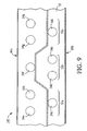
- Each contact array 35a-35c includes a pair of signal contacts, 34a-34b, 34d-34e, 34g-34h, and a reference contact 34c, 34f, 34i.
- Each of the signal contacts, 34a-34b, 34d-34e, 34g-34h, and the corresponding male pins are formed of copper alloy and have an initial characteristic impedance of approximately 50 ohms (single-ended).
- the segment 32 is formed of polyphenylene sulfide (PPS) having a dielectric constant of approximately 3.2.
- PPS polyphenylene sulfide
- Two shield members 60a, 60b are located adjacent to the top and bottom edge of the segment 32.
- Table I provides the spatial orientation between contacts within a group as well as between adjacent groups in order to produce a differential impedance in the first and second signal channels of a mated pair of interconnection devices of approximately 100 ohms.
- Table I Dimension Value A 0.1778 cm B 0.16002 cm C 0.09348 cm D 0.127 cm E 0.12192 cm F 0.21082 cm G 0.381 cm H 0.01016 cm
- the spatial orientation for the mating plug to socket 14 shown in FIG. 7 would have similar spacing in order to properly plug into socket 14.
- the differential impedance of the differential signal channels may be adjusted by inserting material with a different dielectric constant than the segment between the differential signal contacts.
- material with a different dielectric constant for example, an air cavity (air having a dielectric constant of approximately 1) or a Teflon® insert may be inserted between the differential signal contacts in the segment in order to create a composite dielectric having a dielectric constant that is greater or less than the dielectric constant of the segment itself. This will have the effect of lowering or raising the resulting differential impedance between the differential signal contacts on the interconnection device.
- the absolute value of a materials dielectric constant (Er) between adjacent conductors is inversely proportional to the resulting differential impedance between those conductors.
- the lower the resulting dielectric constant (Er) of a composite dielectric material b/w signal contacts the higher the resulting differential impedance between the contacts.
- the higher the resulting dielectric constant (Er) of a composite dielectric material b/w signal contacts the lower the resulting differential impedance between the contacts.
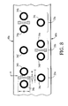
- a plug 14 includes a segment 32 with three contact groupings 35a, 35b, 35c.
- Each contact grouping includes a first signal contact 34a, 34d, 34g, a second signal contact 34b, 34e, 34h, and a reference contact 34c, 34f, 34i.
- a cavity 130a-130c is formed on the segment 32 centered between the first and second signal contact of each grouping. The cavities are open to air and extends from the top surface to approximately 0.28702 cm within the segment 32.
- Table II provides the dimensions of the air cavities shown in FIG. 8 , given the same parameters specified in the description of FIG. 7 . Table II Dimension Value A 0.05334 cm B 0.05334 cm C 0.02794 cm D 0.191262 cm
- the differential impedance of the differential signal channels on the female side of the interconnection device is increased.
- the size and shape of the air cavity will depend on the desired value for the differential impedance of the differential signal channels.
- the desired differential impedance for the first and second signal channels formed by a mating pair of male and female contacts should be 100 Ohms, +/- 5 Ohms.
- the female side alone may have a differential impedance of more or less than 100 Ohms and the male side may have a differential impedance of more or less than 100 Ohms, but the pair when mated have an average differential impedance of 100 Ohms (+/- 5 Ohms).
- Male and female differential impedance values should be equal to eliminate any impedance mismatch (dissimilar impedance values) between the two. Any impedance mismatch usually results in an increased signal reflection of the applied energy back towards the signal source thereby reducing the amount of energy being transmitted through the mated connectors.
- the introduction of a composite dielectric as described herein can minimize the differential impedance mismatch between male and female connectors, thus minimizing reflection of the applied energy back towards the signal source, thereby increasing the amount of energy being transmitted through the mated connectors.
- any material having a different dielectric constant than the segment may be inserted between the signal contacts on either the male or female side.
- a Teflon® insert, air-filled glass balls, or other material having a lower dielectric constant than the material of the segment e.g., PPS resin
- PPS resin material having a lower dielectric constant than the material of the segment
- material with a higher dielectric constant may be added between the signal contacts in order to create a composite dielectric which will raise the dielectric constant of the segment between contacts.
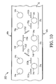
- another interconnection device 140 includes a segment 32 with three contact grouping 35a-35c is shown.
- Each contact grouping includes a pair of differential signal contacts, 34a and 34b, 34d and 34e, 34g and 34h, and a ground reference contact 34c, 34f, 34i.
- a continuous ground plane 150 is disposed within segment 32 and is in contact with each of the reference ground contacts, 34c, 34f, 34i. The ground plane 150 separates the differential signal contacts from each other and will have the effect of raising the differential impedance of each pair of differential signal contacts. Additionally, the ground plane 150 will further reduce cross talk between pairs of differential signal contacts by bleeding off remnant electromagnetic fields generated by electron flow across the differential signal contacts.
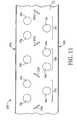
- another interconnection devices 142 include a number of ground planes 152a-152h disposed within the segment 32. Each of the ground planes 152a-152h is configured to electrically connect with the reference ground (Vcc) of the system.
- another interconnection device 144 includes a number of ground planes 154a-154d which are configured to electrically connect with the reference ground of the system.
- the multiple ground planes illustrated in FIGS. 10-11 will effect the differential impedance of the differential signal contacts as well as further reduce cross talk between pairs of differential signal contacts.
- FIGS. 1-11 show a twin-axial arrangement of differential pair contacts within a system using differential signaling.
- the technique for reducing cross-talk using a reference pin connected to ground in close proximity to one or more signal channels is not limited to systems using differential signaling, but could be used in systems using other communication techniques.
- a signal contact and reference contact may be arranged in a pseudo co-axial arrangement where a signal contact and a reference contact form a contact-grouping and do not physically share a common longitudinal axis (as would a traditional co-axial transmission line), but electrically performs like a traditional co-axial transmission line.
- the signal contact and reference contact are physically arranged such that the signal contact and the reference contact are substantially parallel to each other but do not share a common longitudinal axis.
- the reference contacts within the field of contacts will help to absorb electromagnetic fields generated by the signal contacts and may reduce cross-talk between single-ended transmission lines.
- FIGS. 1-11 show contact groupings consisting of three contacts, a first signal contact, second signal contact and reference contact.
- contact groupings in other embodiments may include more or less than three contacts.
- a contact grouping may include a first signal contact and second signal contact (forming differential transmission line), a third and fourth signal contact (forming second differential transmission line) and a reference contact.
- a contact grouping may include one or more signal contacts and a reference contact within the contact grouping.
- the spatial orientation of the contacts within a contact grouping can be selected such that the contacts are electrically equivalent to traditional twin-axial or coaxial wire or cable with respect to cross-sectional construction and electrical signal transmission capabilities. Additionally, the spatial relationship between adjacent contact groupings should be selected to approximate electrical isolation and preserve signal fidelity within a grouping via the reduction of electro-magnetic coupling.
- the arrays of twin-axial contact grouping depicted in FIGS. 1-5 and FIGS. 7-11 are intended to match the multi-layer circuit board routing processes in order to permit the interconnection device, 12, 14, to be mounted to contact pads of printed circuit board without the need for routing with multiple Z-axis escapes as the case with traditional "uniform grid” or "interstitial grid” connector footprints.
- the orientation of the contacts on plug 12 and socket 14 permit it to be mounted and interconnected with the internal circuitry of a multi-layer circuit board using less layers within the circuit board than traditional connectors.
- the interconnection device does not need to be formed of multiple segments with shield members located between adjacent segments as illustrated in FIGS.1-5 and 7-11 .
- a single segment may be created around one or more shield members by forming (e.g., by injection molding) non-conductive resin or other material around one or more shield members.
- the frame may then be formed around the segment and the shield(s) by forming (e.g., by injection molding) a conductive resin or other material around the perimeter of the segment.
- the shield member and frame do not need to be two separate pieces.
- the shield and frame may consist of a one-piece construction with the segment molded or inserted within the single-piece shield-frame member.
- the plug and socket are releasably retained to each other by the mating array of pins and sockets and the mating of the plug and socket frames.
- a clip, pin, screw, bolt, or other means may be used to further secure the plug and socket to each other.
- the interconnection device described herein may be used to connect any array of transmission lines in a digital or analog transmission system, such as an array of transmission lines on a printed circuit board (as illustrated in FIG. 1 ), an active or passive device or a cable bundle.
Landscapes
- Details Of Connecting Devices For Male And Female Coupling (AREA)
- Shielding Devices Or Components To Electric Or Magnetic Fields (AREA)
- Internal Circuitry In Semiconductor Integrated Circuit Devices (AREA)
Claims (46)
- Verbizadungsbauelement (14) für das Aufnehmen einer Anordnung von Kontakten (44a-44c) innerhalb eines digitalen oder analogen Übertragungssystems (10) mit einer elektrischen Erdungsschaltung (114) und einer Chassiserdungsschaltung (120), wobei das Verbindungsbauelement (14) aufweist:ein Segment (32), das aus einem elektrisch isolierenden Material gebildet wird und eine obere und untere Fläche aufweist, wobei das Segment (32) eine Vielzahl von Löchern (33a-33c) umfasst, die auf seiner oberen Fläche angeordnet und in einer vorgegebenen Montagefläche entsprechend der Anordnung von Kontakten (44a-44c) angeordnet sind;ein Abschirmelement (100), das aus einem elektrisch leitenden Material hergestellt und benachbart dem Segment (32) angeordnet und hergestellt wird, um eine elektrische Verbindung zur Chassiserdungsschaltung (120) herzustellen;eine Vielzahl von elektrisch leitenden Kontakten (34), die eine Vielzahl von Signalkontakten (34a, 34b, 34d, 34e, 34g, 34h) aufweisen, die ausgebildet sind, um ein digitales oder analoges Kommunikationssignal zu übertragen, wobei jeder Signalkontakt innerhalb eines Loches (33a-33c) auf der oberen Fläche des Segmentes (32) angeordnet ist, das eine Anordnung von Signalkontakten bildet, und wobei das Abschirmelement (100) benachbart der Anordnung von Signalkontakten angeordnet ist; undeinen Rahmen (30), der aus elektrisch leitendem Material gebildet wird, das mindestens teilweise das Segment (32) umgibt, und in elektrischem Kontakt mit dem Abschinnelement (100) und ausgebildet, um eine elektrische Verbindung mit der Chassiserdungsschaltung (120) herzustellen.
- Verbindungsbauelement (14) nach Anspruch 1, wobei die Vielzahl der elektrisch leitenden Kontakte (34) außerdem eine Vielzahl von Bezugskontakten (34c; 34f; 34i) aufweist, von denen ein jeder innerhalb eines Loches (33c) auf der oberen Fläche des Segmentes (32) angeordnet ist, wobei die Bezugskontakte ausgebildet sind, um elektrisch eine Verbindung zur elektrischen Erdungsschaltung (120) des Systems (10) herzustellen.
- Verbindungsbauelement (14) nach Anspruch 2, bei dem die Vielzahl der Bezugskontakte innerhalb der Anordnung von Signalkontakten angeordnet ist.
- Verbindungsbauelement (14) nach Anspruch 1, das außerdem aufweist:eine Erdungsebene, die mindestens teilweise innerhalb des Segmentes (32) und innerhalb der Anordnung von Signalkontakten angeordnet ist, und wobei die Erdungsebene ausgebildet ist, um elektrisch eine Verbindung mit der elektrischen Erdungsschaltung (114) des Systems (10) herzustellen.
- Verbindungsbauelement (14) nach Anspruch 4, das außerdem aufweist:eine Vielzahl von Erdungsebenen (152a-152h; 154a-154d) , die mindestens teilweise innerhalb des Segmentes (32) und innerhalb der Anordnung von Signalkontakten angeordnet ist, und wobei die Vielzahl der Erdungsebenen ausgebildet ist, um elektrisch eine Verbindung mit der elektrischen Erdungsschaltung (114) des Systems (10) herzustellen.
- Verbindungsbauelement (14) nach Anspruch 1, das außerdem eine Vielzahl von Abschinnelementen (60; 100) aufweist, die benachbart zu den Segmenten (32) angeordnet sind und ein jedes in elektrischem Kontakt mit dem Rahmen (30).
- Verbindungsbauelement (14) nach Anspruch 1, bei dem das Segment (32) mindestens teilweise um das Abschirmelement (100) geformt ist.
- Verbindungsbauelement (14) nach Anspruch 1, bei dem das Segment (32) außerdem mindestens einen mit Luft gefüllten Hohlraum umfasst, der auf dem Segment (32) und innerhalb der Anordnung von Signalkontakten angeordnet ist.
- Verbindungsbauelement (14) nach Anspruch 2, das außerdem ein Arretierelement aufweist, das ausgebildet ist, um die Anordnung von Kontakten mit der Vielzahl von Signalkontakten (34a, 34b) und Bezugskontakten (34c) lösbar zu halten.
- Verbindungsbauelement (14) nach Anspruch 1, bei dem das Verbindungselement aufweist:eine Vielzahl der Segmente (32), wobei Zwischenräume zwischen benachbarten Segmenten (32) mindestens einen Spalt definieren;wobei das Abschirmelement (100), das aus dem elektrisch leitenden Material hergestellt wird, innerhalb mindestens eines Spaltes zwischen benachbarten Segmenten (32) angeordnet wird;eine Vielzahl von Abschirmelementen (100), die aus elektrisch leitendem Material hergestellt werden, die innerhalb einer Vielzahl von Spalten zwischen benachbarten Segmenten (32) angeordnet sind, ausgebildet, um eine elektrische Verbindung mit der Chassiserdungsschaltung (120) des Systems (10) herzustellen; undwobei der Rahmen (30), der aus elektrisch leitendem Material hergestellt wird, die Vielzahl der Segmente (32) umgibt und in elektrischem Kontakt mit der Vielzahl der Abschirmelemente (100).
- Verbindungsbauelement (14) nach Anspruch 10, das außerdem aufweist:eine Vielzahl von elektrisch leitenden Kontakten (34), von denen ein jeder innerhalb eines Loches (33a-33c) auf der oberen Fläche des Segmentes (32) angeordnet und ausgebildet sind, um die Anordnung der Kontakte (44a-44c) lösbar zu halten.
- Verbindungsbauelement (14) nach Anspruch 11, bei dem mindestens einer der Vielzahl von elektrisch leitenden Kontakten (34) ausgebildet ist, um eine elektrische Verbindung mit der elektrischen Erde des Systems (10) herzustellen.
- Verbindungsbauelement (14) nach Anspruch 11, das außerdem aufweist:eine Erdungsebene, die mindestens teilweise innerhalb des Segmentes (32) angeordnet ist, wobei die Erdungsebene ausgebildet ist, um eine elektrische Verbindung mit der Bezugserdungsschaltung (114) des Systems (10) herzustellen.
- Verbindungsbauelement (14) nach Anspruch 1, bei dem die Vielzahl der elektrisch leitenden Kontakte (34) in einer Vielzahl von Vielkontaktgruppierungen (35a, 35b, 35c) angeordnet sind, wobei mindestens eine Vielkontaktgruppierung aufweist:einen ersten Signalkontakt; undeinen Bezugskontakt, der mit einem ersten Abstand vozn ersten Signalkontakt angeordnet und ausgebildet ist, um eine elektrische Verbindung mit der elektrischen Erdungsschaltung (114) des Systems (10) herzustellen;das Abschirmelement (100); undwobei der Rahmen (30), der aus elektrisch leitendem Material hergestellt wird, das Segment (32) umgibt und in elektrischem Kontakt mit dem Abschirinelement (100) und ausgebildet, um eine elektrische Verbindung mit der Chassiserdungsschaltung (120) des Systems (10) herzustellen.
- Verbindungsbauelement (14) nach Anspruch 14, bei dem der erste Signalkontakt und der Eezugskontakt eine Übertragungsleitung bilden, die einer koaxialen Übertragungsleitung elektrisch äquivalent ist.
- Verbindungsbauelement (14) nach Anspruch 14, bei dem eine jede Vielkontaktgruppierung (35a-35c, 34d-34f, 34g-34h) über einen Abstand >= dem ersten Abstand von den benachbarten Vielkoniahgruppierutigen (35a-35c, 34d-34f, 34g-34h) angeordnet ist.
- Verbindungsbauelement (14) nach Anspruch 14, bei dem der erste Signalkontakt ausgebildet ist, um Eintaktsignale zu übertragen.
- Verbindungsbauelement (14) nach Anspruch 14, das außerdem aufweist:ein zweites Signalkontaktelement, das mit einem zweiten Abstand vom ersten elektrischen Signalkontakt angeordnet ist.
- Verbindungsbauelement (14) nach Anspruch 18, bei dem der erste und zweite Sigualkontakt (34) eine Übertragungsleitung bilden, die einer Twinaxial-Differentialubertragungsleitung elektrisch äquivalent ist.
- Verbindungsbauelement (14) nach Anspruch 18, bei dem eine jede Vielkontaktgruppierung (35a, 35b, 35c) über einen Abstand >= dem zweiten Abstand von den benachbarten Vielkontaktgruppierungen (35a, 35b, 35c) angeordnet ist.
- Verbindungsbauelement (14) nach Anspruch 20, bei dem der erste Abstand > als der zweite Abstand ist.
- Verbindungsbauelement (14) nach Anspruch 20, bei dem der erste Abstand = dem zweiten Abstand ist.
- Verbindungsbauelement (14) nach Anspruch 14, bei dem der erste und zweite Signalkontakt innerhalb einer jeden Vielkontaktgruppierung (35a, 35b, 35c) ausgebildet sind, um ungleiche Eintaktsignale zu übertragen.
- Verbindungsbauelement (14) nach Anspruch 14, bei dem der erste und zweite Signalkontakt im Wesentlichen den gleichen Querschnitt aufweisen.
- Verbindungsbauelement (14) nach Anspruch 24, bei dem der erste Signal-, zweite Signal- und der Bezugskontakt (34a-34c) im Wesentlichen den gleichen Querschnitt aufweisen.
- Verbindungsbauelement (14) nach Anspruch 14, bei dem der erste und zweite Signalkontakt (34a, 34b) im Wesentlichen die gleiche anfängliche charakteristische Impedanz aufweisen.
- Verbindungsbauelement (14) nach Anspruch 19, bei dem der erste und zweite Signalkontakt (34a, 34b) innerhalb einer jeden Vielkontaktgruppierung (35a, 35b, 35c) ausgebildet sind, um Niederspannungsdifferentialsignale zu übertragen.
- Verbindungsbauelement (14) nach Anspruch 27, bei dem die Differenzimpedanz des ersten und zweiten Signalkontaktes (34a, 34b) innerhalb einer jeden Vielkontakgruppierung (35a, 35b, 35c) annähernd 100 Ohm beträgt.
- Verbindungsbauelement (14) nach Anspruch 14, das außerdem aufweist:eine Vielzahl von Segmenten (32), die aus elektrisch isolierendem Material hergestellt werden, wobei die Zwischenräume zwischen benachbarten Segmenten (32) mindestens einen Spalt definieren, wobei jedes Segment (32) eine obere und untere Fläche aufweist und eine Vielzahl von Löchern (33a-33c) umfasst, die auf seiner oberen Fläche angeordnet und in einer vorgegebenen Montagefläche entsprechend der Anordnung der Kontakte (44a-44c) angeordnet sind; undein Absehirmelement (100), das aus elektrisch leitendem Material hergestellt wird, angeordnet innerhalb mindestens eines Spaltes zwischen benachbarten Segmenten (32) und in elektrischem Kontakt mit der elektrischen Erde des Systems (10).
- Verbindungsbauelement (14) nach Anspruch 29, das außerdem aufweist:einen Rahmen (30), der aus elektrisch leitendem Material hergestellt wird, das die Vielzahl der Segmente (32) umgibt, und in elektrischem Kontakt mit der Vielzahl der Abschirmelemente (100) und ausgebildet, um eine elektrische Verbindung mit der Chassiserdungsschaltung (120) des Systems (10) herzustellen.
- Verbindungsbauelement (14) nach Anspruch 14, das außerdem aufweist:eine Erdungsebene, die mindestens teilweise innerhalb des Segmentes (32) angeordnet ist, wobei die Erdungsebene ausgebildet ist, um eine elektrische Verbindung mit der Bezugserdungsschaltung (114) des Systems (10) herzustellen.
- Leiterkarte für eine Verwendung in einem digitalen oder analogen Übertragungssystem (10) mit einer elektrischen Erdungsschaltung (114) und einer Chassiserdungsschaltung (120), wobei die Leiterkarte aufweist:eine Leiterplatte (18) mit einer Vielzahl von Kontaktanschlussflächen, die in einer vorgegebenen Montagefläche angeordnet sind; undein Verbindungsbauelement (14), das aufweist:ein Segment (32) mit einer oberen und unteren Fläche, wobei das Segment (32) eine Vielzahl von Löchern (33a-33c) aufweist, die sich durch die obere und untere Fläche erstrecken und in einer vorgegebenen Montagefläche angeordnet sind, um zu der vorgegebenen Montagefläche der Vielzahl von Obefflächemnontageauschlussflächen zu passen;eine Vielzahl von elektrisch leitenden Kontaktelementen (34), die in einem jeden der Löcher (33a-33c) angeordnet und elektrisch mit ihrer jeweiligen Oberflächenmontageanschlussfläche verbunden sind;ein Abschirmelement (100), das aus einem elektrisch leitenden Material hergestellt und benachbart dem Segment (32) angeordnet,einen Rahmen (30), der aus elektrisch leitendem Material hergestellt wird, das das Segment (32) umgibt, wobei der Rahmen (30) elektrisch mit dem Absehirmslement (100) und mit der Chassiserdungsschaltung (120) des Systems (10) verbunden ist.
- Leiterkarte nach Anspruch 32, bei der die Vielzahl der Kontakte (34) in einer Vielzahl von Vielkontaktgruppierungen (35a, 35b, 35c) angeordnet ist, wobei eine jede Vielkontaktgruppierung aufweist:einen ersten Signalkontakt; undeinen Bezugskontakt, der mit einem ersten Abstand vom ersten elektrisch leitenden Kontakt angeordnet und mit der elektrischen Erdungsschaltung (114) des Systems (10) verbunden ist.
- Leiterkarte nach Anspruch 33, bei der die Vielkontaktgruppierung (35a, 35b, 35c) außerdem ausweist:einen zweiten Signalkontakt, der mit einem zweiten Abstand vom ersten elektrisch leitenden Kontakt angeordnet ist.
- Leiterkarte nach Anspruch 33, bei der das Verbindungsbauelement (14) außerdem aufweist:eine Erdungsebene, die mindestens teilweise innerhalb des Segmentes (32) angeordnet ist, wobei die Erdungsebene ausgebildet ist, um eine elektrische Verbindung mit der Bezugserdungsschaltung (114) des Systems (10) herzustellen.
- Leiterkarte nach Anspruch 34, bei der der erste und zweite elektrisch leitende Kontakt (34) eine Übertragungsleitung bilden, die elektrisch der Twinaxial-Differentialübertragungsleitung äquivalent ist.
- Verbindungsbauelement (14) nach Anspruch 1, wobei das Verbindungsbauelement aufweist:das Segment (32), das aus dem Material mit einer Dielektrizitätskonstante Er1 hergestellt wird;wobei die Vielzahl der Kontakte aufweist:einen ersten Signalkontakt, der in einem ersten Loch auf dem Segment (32) angeordnet ist; undeinen zweiten Signalkontakt, der in einem zweiten Loch auf dem Segment (32) angeordnet ist, benachbart dem ersten Loch, in dem der erste Signalkoniakt angeordnet ist, und wobei ein Hohlraum im Segment (32) zwischen dem ersten und zweiten Loch gebildet wird.
- Verbindungsbauelement (14) nach Anspruch 37, bei dem der Hohlraum auf der oberen Fläche des Segmentes (32) gebildet wird und für Luft offen ist.
- Verbindungsbauelement (14) nach Anspruch 37, das außerdem einen Einsatz aufweist, der aus einem Material mit einer Dielektrizitätskonstante von Er2 hergestellt wird, wobei der Einsatz innerhalb des Hohlraumes angeordnet wird.
- Verbindungsbauelement (14) nach Anspruch 39, bei dem Er1, > Er2-
- Verbindungsbauelement (14) nach Anspruch 39, bei dem Er1 < Er2.
- Verbindungsbauelement (14) nach Anspruch 37, bei dem der Hohlraum innerhalb des Segmentes (32) gebildet und mit einem dielektrischen Material gefüllt wird.
- Verbindungsbauelement (14) nach Anspruch 42, bei dem das dielektrische Material Luft ist.
- Verbindungsbauelement (14) nach Anspruch 37, das eine Vielzahl von ersten Signalkontakten, die in einer Vielzahl von Löchern (33a-33c) angeordnet sind, und eine Vielzahl von zweiten Signalkontakten aufweist, die jeweils in einem Loch angeordnet sind, das einem Loch benachbart ist, das einen ersten Signalkontakt enthält, wobei die Vielzahl der ersten und zweiten Signalkontakte eine Anordnung von Signalkontakten (34) bildet, und wobei ein Hohlraum im Segment (32) zwischen einem jeden Paar von ersten und zweiten Signaücozxtakten gebildet wird.
- Verbindungsbauelement (14) nach Anspruch 44, das außerdem eine Vielzahl von Erdungskontakten auiweist, die in einer Vielzahl von Löchern (33a-33c) auf dem Segment (32) angeordnet sind, und die innerhalb der Signalkontakte angeordnet sind, wobei die Vielzahl der Erdungskontakte eine elektrische Verbindung mit der elektrischen Erdungssebaltung (114) des Systems (10) herstellt.
- Verbindungsbauelement (14) nach Anspruch 44, das außerdem eine Erdungsabschirmung aufweist, die beim Segment (32) angeordnet und ausgebildet ist, um eine elektrische Verbindung mit der elektrischen Erdungsschaltung (114) des Systems (10) herzustellen.
Applications Claiming Priority (3)
| Application Number | Priority Date | Filing Date | Title |
|---|---|---|---|
| US10/178,957 US6743049B2 (en) | 2002-06-24 | 2002-06-24 | High speed, high density interconnection device |
| US178957 | 2002-06-24 | ||
| PCT/US2003/019830 WO2004001912A1 (en) | 2002-06-24 | 2003-06-24 | High speed, high density interconnection device |
Publications (3)
| Publication Number | Publication Date |
|---|---|
| EP1540779A1 EP1540779A1 (de) | 2005-06-15 |
| EP1540779A4 EP1540779A4 (de) | 2010-01-06 |
| EP1540779B1 true EP1540779B1 (de) | 2012-03-21 |
Family
ID=29734826
Family Applications (1)
| Application Number | Title | Priority Date | Filing Date |
|---|---|---|---|
| EP03761284A Expired - Lifetime EP1540779B1 (de) | 2002-06-24 | 2003-06-24 | Schnelle, dichte verbindungseinrichtung |
Country Status (7)
| Country | Link |
|---|---|
| US (4) | US6743049B2 (de) |
| EP (1) | EP1540779B1 (de) |
| JP (1) | JP4434947B2 (de) |
| AT (1) | ATE550811T1 (de) |
| AU (1) | AU2003249355A1 (de) |
| CA (1) | CA2490096C (de) |
| WO (1) | WO2004001912A1 (de) |
Families Citing this family (61)
| Publication number | Priority date | Publication date | Assignee | Title |
|---|---|---|---|---|
| SG71046A1 (en) | 1996-10-10 | 2000-03-21 | Connector Systems Tech Nv | High density connector and method of manufacture |
| US6918776B2 (en) * | 2003-07-24 | 2005-07-19 | Fci Americas Technology, Inc. | Mezzanine-type electrical connector |
| US7145083B2 (en) * | 2004-07-13 | 2006-12-05 | Nortel Networks Limited | Reducing or eliminating cross-talk at device-substrate interface |
| US20060051989A1 (en) * | 2004-09-08 | 2006-03-09 | Advanced Interconnections Corporation | Multiple piece shroud |
| JP3143222U (ja) * | 2004-12-22 | 2008-07-17 | モレックス インコーポレーテッド | 改良されたデュアルビームコンタクトを備えたコネクタ |
| US7077658B1 (en) * | 2005-01-05 | 2006-07-18 | Avx Corporation | Angled compliant pin interconnector |
| EP1872443A1 (de) * | 2005-03-31 | 2008-01-02 | Molex Incorporated | Dichter robuster verbinder mit aussparungen |
| CN1889808A (zh) * | 2005-06-28 | 2007-01-03 | 鸿富锦精密工业(深圳)有限公司 | 印刷电路板重叠焊盘的布线结构 |
| US7247058B2 (en) * | 2005-08-25 | 2007-07-24 | Tyco Electronics Corporation | Vertical docking connector |
| US7262974B2 (en) * | 2005-10-28 | 2007-08-28 | Cisco Technology, Inc. | Techniques for alleviating the need for DC blocking capacitors in high-speed differential signal pairs |
| US7361022B2 (en) * | 2006-06-26 | 2008-04-22 | Lotes Co., Ltd. | Electrical connector |
| US20080009148A1 (en) * | 2006-07-07 | 2008-01-10 | Glenn Goodman | Guided pin and plunger |
| US7553170B2 (en) * | 2006-12-19 | 2009-06-30 | Fci Americas Technology, Inc. | Surface mount connectors |
| US7484964B2 (en) * | 2007-06-07 | 2009-02-03 | Hon Hai Precision Ind. Co., Ltd. | Electrical connector assembly with floatably arranged wafer |
| DE102007045903B3 (de) * | 2007-09-26 | 2009-01-02 | Amphenol-Tuchel Electronics Gmbh | Hochpoliger Matrixsteckverbinder |
| US7671273B2 (en) * | 2007-10-09 | 2010-03-02 | International Business Machines Corporation | Method and apparatus for facilitating signal transmission using differential transmission lines |
| CN102047507B (zh) * | 2008-06-04 | 2013-04-24 | 星电株式会社 | 电连接器 |
| US7740489B2 (en) * | 2008-10-13 | 2010-06-22 | Tyco Electronics Corporation | Connector assembly having a compressive coupling member |
| US7637777B1 (en) | 2008-10-13 | 2009-12-29 | Tyco Electronics Corporation | Connector assembly having a noise-reducing contact pattern |
| US7736183B2 (en) * | 2008-10-13 | 2010-06-15 | Tyco Electronics Corporation | Connector assembly with variable stack heights having power and signal contacts |
| US7867032B2 (en) * | 2008-10-13 | 2011-01-11 | Tyco Electronics Corporation | Connector assembly having signal and coaxial contacts |
| US7896698B2 (en) * | 2008-10-13 | 2011-03-01 | Tyco Electronics Corporation | Connector assembly having multiple contact arrangements |
| US8366485B2 (en) | 2009-03-19 | 2013-02-05 | Fci Americas Technology Llc | Electrical connector having ribbed ground plate |
| US8113851B2 (en) * | 2009-04-23 | 2012-02-14 | Tyco Electronics Corporation | Connector assemblies and systems including flexible circuits |
| US8123531B2 (en) * | 2009-09-10 | 2012-02-28 | Kabushiki Kaisha Toshiba | Card holder and broadcast receiving apparatus having card holder |
| US8109767B2 (en) * | 2010-01-20 | 2012-02-07 | Lotes Co., Ltd. | Electrical connector |
| JP5564288B2 (ja) * | 2010-03-01 | 2014-07-30 | 株式会社フジクラ | コネクタアッセンブリ |
| US7918683B1 (en) | 2010-03-24 | 2011-04-05 | Tyco Electronics Corporation | Connector assemblies and daughter card assemblies configured to engage each other along a side interface |
| US20120106052A1 (en) * | 2010-10-29 | 2012-05-03 | Odineal Robert D | Twin-mate cpu assembly |
| EP2518835B1 (de) * | 2011-04-28 | 2019-01-16 | Harman Becker Automotive Systems GmbH | Elektrischer Steckverbinder |
| TWI473357B (zh) * | 2011-08-23 | 2015-02-11 | Hon Hai Prec Ind Co Ltd | 電連接器及其製造方法 |
| SE536156C2 (sv) * | 2011-09-14 | 2013-06-04 | Bae Systems Haegglunds Ab | Kretskortskonfiguration |
| US8597047B2 (en) * | 2011-11-14 | 2013-12-03 | Airborn, Inc. | Insulator with air dielectric cavities for electrical connector |
| EP2624034A1 (de) | 2012-01-31 | 2013-08-07 | Fci | Abbaubare optische Kupplungsvorrichtung |
| USD727268S1 (en) | 2012-04-13 | 2015-04-21 | Fci Americas Technology Llc | Vertical electrical connector |
| US9257778B2 (en) | 2012-04-13 | 2016-02-09 | Fci Americas Technology | High speed electrical connector |
| US8944831B2 (en) | 2012-04-13 | 2015-02-03 | Fci Americas Technology Llc | Electrical connector having ribbed ground plate with engagement members |
| USD718253S1 (en) | 2012-04-13 | 2014-11-25 | Fci Americas Technology Llc | Electrical cable connector |
| USD727852S1 (en) | 2012-04-13 | 2015-04-28 | Fci Americas Technology Llc | Ground shield for a right angle electrical connector |
| JP5857892B2 (ja) | 2012-07-03 | 2016-02-10 | 株式会社オートネットワーク技術研究所 | 多極コネクタ |
| USD751507S1 (en) | 2012-07-11 | 2016-03-15 | Fci Americas Technology Llc | Electrical connector |
| US9543703B2 (en) | 2012-07-11 | 2017-01-10 | Fci Americas Technology Llc | Electrical connector with reduced stack height |
| USD745852S1 (en) | 2013-01-25 | 2015-12-22 | Fci Americas Technology Llc | Electrical connector |
| USD720698S1 (en) | 2013-03-15 | 2015-01-06 | Fci Americas Technology Llc | Electrical cable connector |
| CN104183959B (zh) * | 2013-05-28 | 2017-09-22 | 中航光电科技股份有限公司 | 具有高差分特性阻抗的电连接器 |
| US8975735B2 (en) * | 2013-08-08 | 2015-03-10 | Infineon Technologies Ag | Redistribution board, electronic component and module |
| US20150325954A1 (en) * | 2014-05-06 | 2015-11-12 | Tyco Electronics Corporation | Substrate with a low dielectric constant material and method of molding |
| CN106299774B (zh) * | 2016-09-18 | 2018-07-10 | 珠海格力电器股份有限公司 | 电路对接装置及空调器 |
| US10050361B1 (en) * | 2017-05-22 | 2018-08-14 | Te Connectivity Corporation | Flexible circuit connector |
| CN112117605B (zh) * | 2017-09-29 | 2022-03-11 | 中航光电科技股份有限公司 | 一种连接器及其信号传输结构 |
| US11160163B2 (en) * | 2017-11-17 | 2021-10-26 | Texas Instruments Incorporated | Electronic substrate having differential coaxial vias |
| JP6988864B2 (ja) * | 2017-12-21 | 2022-01-05 | 株式会社オートネットワーク技術研究所 | シールド端子 |
| US10644421B2 (en) * | 2018-06-27 | 2020-05-05 | Aptiv Technologies Limited | Electrical connector with dielectric properties suitable for high speed data transmission |
| CN209344444U (zh) * | 2019-01-18 | 2019-09-03 | 富顶精密组件(深圳)有限公司 | 电连接器组合 |
| US11177553B2 (en) | 2019-05-03 | 2021-11-16 | Qualcomm Incorporated | Interface connector for supporting millimeter wave wireless communications |
| DE102019130774A1 (de) * | 2019-11-14 | 2021-05-20 | Rosenberger Hochfrequenztechnik Gmbh & Co. Kg | Mehrfachverbinder, Baugruppenverbindung und Verfahren sowie Vorrichtung zur Herstellung eines Mehrfachverbinders |
| US11742605B2 (en) | 2019-11-20 | 2023-08-29 | Lawrence Livermore National Security, Llc | Apparatus and method for high density detachable electrical interface |
| JP7417855B2 (ja) | 2020-01-15 | 2024-01-19 | パナソニックIpマネジメント株式会社 | コネクタ装置 |
| JP7403085B2 (ja) * | 2020-01-15 | 2023-12-22 | パナソニックIpマネジメント株式会社 | コネクタ及びコネクタ装置 |
| US12470010B2 (en) * | 2021-08-23 | 2025-11-11 | Te Connectivity Solutions Gmbh Et Al. | Housing having different dielectric constants |
| CN217983967U (zh) * | 2022-08-17 | 2022-12-06 | 天津莱尔德电子材料有限公司 | 通信接口 |
Family Cites Families (67)
| Publication number | Priority date | Publication date | Assignee | Title |
|---|---|---|---|---|
| US3904265A (en) * | 1972-02-23 | 1975-09-09 | Amp Inc | Electrical connector shield having an internal cable clamp |
| US4239318A (en) * | 1979-07-23 | 1980-12-16 | International Telephone And Telegraph Corporation | Electrical connector shield |
| JPS57160101U (de) * | 1981-03-31 | 1982-10-07 | ||
| US4433886A (en) * | 1981-12-17 | 1984-02-28 | Elco Corporation | Connector mounting for integrated circuit chip packages |
| US4449778A (en) * | 1982-12-22 | 1984-05-22 | Amp Incorporated | Shielded electrical connector |
| JPS6288383A (ja) | 1985-10-15 | 1987-04-22 | Toshiba Corp | ホ−ル素子 |
| JPS62154588A (ja) * | 1985-12-27 | 1987-07-09 | ヒロセ電機株式会社 | 電気コネクタ用シ−ルドケ−スおよびその製造方法 |
| JPS6321772A (ja) * | 1986-07-15 | 1988-01-29 | ヒロセ電機株式会社 | 電気コネクタ用シールドケース |
| JPH0339901Y2 (de) * | 1987-04-30 | 1991-08-22 | ||
| US4974075A (en) * | 1987-08-11 | 1990-11-27 | Olympus Optical Co., Ltd. | Image pickup apparatus having connector capable of separately shielding grouped electrical connections |
| US4808126A (en) * | 1987-10-05 | 1989-02-28 | Itt Corporation | Electrical connector shield |
| US5282268A (en) * | 1988-09-27 | 1994-01-25 | Allen-Bradley Company, Inc. | Video image storage system |
| US4909743A (en) * | 1988-10-14 | 1990-03-20 | Teradyne, Inc. | Electrical connector |
| US4898546A (en) * | 1988-12-16 | 1990-02-06 | E. I. Du Pont De Nemours And Company | Ground plane shield device for right angle connectors |
| AU7736691A (en) * | 1990-06-08 | 1991-12-12 | E.I. Du Pont De Nemours And Company | Connectors with ground structure |
| US5133679A (en) * | 1990-06-08 | 1992-07-28 | E. I. Du Pont De Nemours And Company | Connectors with ground structure |
| US5055069A (en) * | 1990-06-08 | 1991-10-08 | E. I. Du Pont De Nemours And Company | Connectors with ground structure |
| JPH06505359A (ja) | 1991-01-30 | 1994-06-16 | ラビナル コンポーネンツ アンド システムズ,インコーポレイティド | 電気コネクタ |
| US5310354A (en) * | 1992-03-20 | 1994-05-10 | E. I. Du Pont De Nemours And Company | Integral ground terminal and tail shield |
| JPH05275139A (ja) | 1992-03-25 | 1993-10-22 | Toshiba Corp | コネクタ |
| JP2910390B2 (ja) | 1992-03-31 | 1999-06-23 | 日本電気株式会社 | コネクタ |
| US5215473A (en) | 1992-05-05 | 1993-06-01 | Molex Incorporated | High speed guarded cavity backplane connector |
| US5256086A (en) * | 1992-12-04 | 1993-10-26 | Molex Incorporated | Electrical connector shield and method of fabricating same |
| US5331505A (en) * | 1993-01-08 | 1994-07-19 | Honeywell Inc. | Multi-coplanar capacitor for electrical connector |
| US5409400A (en) * | 1993-01-15 | 1995-04-25 | The Whitaker Corporation | Shielding for an electrical connector |
| US5360349A (en) * | 1993-03-31 | 1994-11-01 | Teradyne, Inc. | Power connector |
| US5403206A (en) * | 1993-04-05 | 1995-04-04 | Teradyne, Inc. | Shielded electrical connector |
| NL9400321A (nl) * | 1994-03-03 | 1995-10-02 | Framatome Connectors Belgium | Connector voor een kabel voor hoogfrequente signalen. |
| US5748449A (en) * | 1995-04-20 | 1998-05-05 | Sierra Wireless, Inc. | Electrical enclosure for radio |
| US5702255A (en) * | 1995-11-03 | 1997-12-30 | Advanced Interconnections Corporation | Ball grid array socket assembly |
| US5672064A (en) * | 1995-12-21 | 1997-09-30 | Teradyne, Inc. | Stiffener for electrical connector |
| US5702258A (en) | 1996-03-28 | 1997-12-30 | Teradyne, Inc. | Electrical connector assembled from wafers |
| JPH09283247A (ja) | 1996-04-04 | 1997-10-31 | Minnesota Mining & Mfg Co <3M> | Icソケット |
| US5795191A (en) | 1996-09-11 | 1998-08-18 | Preputnick; George | Connector assembly with shielded modules and method of making same |
| SG71046A1 (en) | 1996-10-10 | 2000-03-21 | Connector Systems Tech Nv | High density connector and method of manufacture |
| US5969944A (en) * | 1996-12-31 | 1999-10-19 | Intel Corporation | Method and apparatus for mounting a very large scale integration (VLSI) chip package to a computer chasis for cooling |
| US5993259A (en) * | 1997-02-07 | 1999-11-30 | Teradyne, Inc. | High speed, high density electrical connector |
| US5997361A (en) * | 1997-06-30 | 1999-12-07 | Litton Systems, Inc. | Electronic cable connector |
| US6011691A (en) * | 1998-04-23 | 2000-01-04 | Lockheed Martin Corporation | Electronic component assembly and method for low cost EMI and capacitive coupling elimination |
| DE19919140B4 (de) * | 1998-04-29 | 2011-03-31 | National Semiconductor Corp.(N.D.Ges.D.Staates Delaware), Santa Clara | Niederspannungs-Differenzsignaltreiber mit Vorverstärkerschaltung |
| US6179663B1 (en) * | 1998-04-29 | 2001-01-30 | Litton Systems, Inc. | High density electrical interconnect system having enhanced grounding and cross-talk reduction capability |
| TW374502U (en) * | 1998-06-10 | 1999-11-11 | Hon Hai Prec Ind Co Ltd | Power connector of covered style |
| JP2000050783A (ja) | 1998-08-05 | 2000-02-22 | Hiroshi Kiue | 高枝切り用の鋏と兼用のスプレー缶入農薬等散布器具 |
| DE69929384T2 (de) * | 1998-10-09 | 2006-08-31 | Sumitomo Wiring Systems, Ltd., Yokkaichi | Gitterleiterplatte |
| US6530790B1 (en) | 1998-11-24 | 2003-03-11 | Teradyne, Inc. | Electrical connector |
| JP2000223218A (ja) * | 1999-01-27 | 2000-08-11 | Mitsumi Electric Co Ltd | 小型コネクタ |
| JP4334662B2 (ja) * | 1999-04-07 | 2009-09-30 | 日本圧着端子製造株式会社 | Icカード用フレームキットおよびicカード |
| US6454605B1 (en) * | 1999-07-16 | 2002-09-24 | Molex Incorporated | Impedance-tuned termination assembly and connectors incorporating same |
| US6213787B1 (en) * | 1999-12-16 | 2001-04-10 | Advanced Interconnections Corporation | Socket/adapter system |
| US6533613B1 (en) * | 1999-12-20 | 2003-03-18 | Intel Corporation | Shielded zero insertion force socket |
| DE60107388T2 (de) * | 2000-02-03 | 2005-12-15 | Teradyne Inc., Boston | Steckverbinder mit abschirmung |
| US6293827B1 (en) * | 2000-02-03 | 2001-09-25 | Teradyne, Inc. | Differential signal electrical connector |
| US6371773B1 (en) * | 2000-03-23 | 2002-04-16 | Ohio Associated Enterprises, Inc. | High density interconnect system and method |
| US6350134B1 (en) * | 2000-07-25 | 2002-02-26 | Tyco Electronics Corporation | Electrical connector having triad contact groups arranged in an alternating inverted sequence |
| US7136833B1 (en) | 2000-09-25 | 2006-11-14 | Eugene Lawrence Podsiadlo | Communication network based system and method for auctioning shares on an investment product |
| US20020125967A1 (en) * | 2000-11-03 | 2002-09-12 | Garrett Richard H. | Air dielectric backplane interconnection system |
| US6843657B2 (en) | 2001-01-12 | 2005-01-18 | Litton Systems Inc. | High speed, high density interconnect system for differential and single-ended transmission applications |
| US6482038B2 (en) * | 2001-02-23 | 2002-11-19 | Fci Americas Technology, Inc. | Header assembly for mounting to a circuit substrate |
| US20030022555A1 (en) * | 2001-03-30 | 2003-01-30 | Samtec, Inc. | Ground plane shielding array |
| US6739028B2 (en) * | 2001-07-13 | 2004-05-25 | Hrl Laboratories, Llc | Molded high impedance surface and a method of making same |
| US6981883B2 (en) * | 2001-11-14 | 2006-01-03 | Fci Americas Technology, Inc. | Impedance control in electrical connectors |
| US6635958B2 (en) * | 2001-12-03 | 2003-10-21 | Dover Capital Formation Group | Surface mount ceramic package |
| US6699048B2 (en) * | 2002-01-14 | 2004-03-02 | Fci Americas Technology, Inc. | High density connector |
| US6747216B2 (en) * | 2002-02-04 | 2004-06-08 | Intel Corporation | Power-ground plane partitioning and via connection to utilize channel/trenches for power delivery |
| US6739885B2 (en) * | 2002-05-21 | 2004-05-25 | Tyco Electronics Corporation | Filtered and shielded electrical connector |
| US6776629B2 (en) * | 2002-06-13 | 2004-08-17 | Fci Americas Technology, Inc. | Connector for mounting to mating connector, and shield therefor |
| AU2003245636A1 (en) * | 2002-06-21 | 2004-01-06 | Molex Incorporated | High-density, impedance-tuned connector having modular construction |
-
2002
- 2002-06-24 US US10/178,957 patent/US6743049B2/en not_active Expired - Lifetime
-
2003
- 2003-06-24 AU AU2003249355A patent/AU2003249355A1/en not_active Abandoned
- 2003-06-24 AT AT03761284T patent/ATE550811T1/de active
- 2003-06-24 CA CA2490096A patent/CA2490096C/en not_active Expired - Fee Related
- 2003-06-24 WO PCT/US2003/019830 patent/WO2004001912A1/en not_active Ceased
- 2003-06-24 JP JP2004516178A patent/JP4434947B2/ja not_active Expired - Fee Related
- 2003-06-24 EP EP03761284A patent/EP1540779B1/de not_active Expired - Lifetime
-
2004
- 2004-02-25 US US10/786,248 patent/US6899550B2/en not_active Expired - Lifetime
- 2004-04-08 US US10/820,296 patent/US7021945B2/en not_active Expired - Lifetime
-
2006
- 2006-04-04 US US11/397,334 patent/US8109770B2/en not_active Expired - Fee Related
Also Published As
| Publication number | Publication date |
|---|---|
| WO2004001912A1 (en) | 2003-12-31 |
| JP2005531122A (ja) | 2005-10-13 |
| US7021945B2 (en) | 2006-04-04 |
| CA2490096C (en) | 2011-08-16 |
| CA2490096A1 (en) | 2003-12-31 |
| US20030236031A1 (en) | 2003-12-25 |
| ATE550811T1 (de) | 2012-04-15 |
| EP1540779A1 (de) | 2005-06-15 |
| US6743049B2 (en) | 2004-06-01 |
| US8109770B2 (en) | 2012-02-07 |
| US6899550B2 (en) | 2005-05-31 |
| US20040166704A1 (en) | 2004-08-26 |
| US20060240688A1 (en) | 2006-10-26 |
| JP4434947B2 (ja) | 2010-03-17 |
| HK1078172A1 (en) | 2006-03-03 |
| EP1540779A4 (de) | 2010-01-06 |
| US20040192089A1 (en) | 2004-09-30 |
| AU2003249355A1 (en) | 2004-01-06 |
Similar Documents
| Publication | Publication Date | Title |
|---|---|---|
| EP1540779B1 (de) | Schnelle, dichte verbindungseinrichtung | |
| CN102598431B (zh) | 具有接地板和接地结合杆的电连接器 | |
| TWI847482B (zh) | 電纜線連接器 | |
| US7651373B2 (en) | Board-to-board electrical connector | |
| US6910897B2 (en) | Interconnection system | |
| US6905367B2 (en) | Modular coaxial electrical interconnect system having a modular frame and electrically shielded signal paths and a method of making the same | |
| US9431768B1 (en) | Electrical connector having resonance control | |
| EP1311038A2 (de) | Verbinder für hohe Übertragungsgeschwindigkeiten | |
| US10027061B2 (en) | Socket with insert-molded terminal | |
| US10249988B2 (en) | Paddle card having shortened signal contact pads | |
| CN109565122B (zh) | 直接附连连接器 | |
| CN1227005A (zh) | 高频电连接器 | |
| US20190356089A1 (en) | Electrical connector assembly for a communication system | |
| HK1078172B (en) | High speed, high density interconnection device | |
| WO2021207479A1 (en) | High-speed electrical connector |
Legal Events
| Date | Code | Title | Description |
|---|---|---|---|
| PUAI | Public reference made under article 153(3) epc to a published international application that has entered the european phase |
Free format text: ORIGINAL CODE: 0009012 |
|
| 17P | Request for examination filed |
Effective date: 20050124 |
|
| AK | Designated contracting states |
Kind code of ref document: A1 Designated state(s): AT BE BG CH CY CZ DE DK EE ES FI FR GB GR HU IE IT LI LU MC NL PT RO SE SI SK TR |
|
| AX | Request for extension of the european patent |
Extension state: AL LT LV MK |
|
| DAX | Request for extension of the european patent (deleted) | ||
| REG | Reference to a national code |
Ref country code: HK Ref legal event code: DE Ref document number: 1078172 Country of ref document: HK |
|
| A4 | Supplementary search report drawn up and despatched |
Effective date: 20091209 |
|
| RIC1 | Information provided on ipc code assigned before grant |
Ipc: H01R 12/16 20060101ALI20091203BHEP Ipc: H01R 13/658 20060101ALI20091203BHEP Ipc: H01R 13/648 20060101AFI20040114BHEP |
|
| 17Q | First examination report despatched |
Effective date: 20101220 |
|
| RIC1 | Information provided on ipc code assigned before grant |
Ipc: H01R 13/658 20110101ALI20110720BHEP Ipc: H01R 13/648 20060101AFI20110720BHEP Ipc: H01R 12/71 20110101ALI20110720BHEP |
|
| REG | Reference to a national code |
Ref country code: DE Ref legal event code: R079 Ref document number: 60340354 Country of ref document: DE Free format text: PREVIOUS MAIN CLASS: H01R0013648000 Ipc: H01R0013658000 |
|
| GRAP | Despatch of communication of intention to grant a patent |
Free format text: ORIGINAL CODE: EPIDOSNIGR1 |
|
| RIC1 | Information provided on ipc code assigned before grant |
Ipc: H01R 12/71 20110101ALI20110830BHEP Ipc: H01R 13/6461 20110101ALI20110830BHEP Ipc: H01R 13/658 20110101AFI20110830BHEP |
|
| GRAS | Grant fee paid |
Free format text: ORIGINAL CODE: EPIDOSNIGR3 |
|
| GRAA | (expected) grant |
Free format text: ORIGINAL CODE: 0009210 |
|
| AK | Designated contracting states |
Kind code of ref document: B1 Designated state(s): AT BE BG CH CY CZ DE DK EE ES FI FR GB GR HU IE IT LI LU MC NL PT RO SE SI SK TR |
|
| REG | Reference to a national code |
Ref country code: GB Ref legal event code: FG4D |
|
| REG | Reference to a national code |
Ref country code: CH Ref legal event code: EP |
|
| REG | Reference to a national code |
Ref country code: IE Ref legal event code: FG4D |
|
| REG | Reference to a national code |
Ref country code: AT Ref legal event code: REF Ref document number: 550811 Country of ref document: AT Kind code of ref document: T Effective date: 20120415 |
|
| REG | Reference to a national code |
Ref country code: DE Ref legal event code: R096 Ref document number: 60340354 Country of ref document: DE Effective date: 20120516 |
|
| REG | Reference to a national code |
Ref country code: CH Ref legal event code: NV Representative=s name: MARKS & CLERK (LUXEMBOURG) LLP |
|
| REG | Reference to a national code |
Ref country code: NL Ref legal event code: VDEP Effective date: 20120321 |
|
| PG25 | Lapsed in a contracting state [announced via postgrant information from national office to epo] |
Ref country code: GR Free format text: LAPSE BECAUSE OF FAILURE TO SUBMIT A TRANSLATION OF THE DESCRIPTION OR TO PAY THE FEE WITHIN THE PRESCRIBED TIME-LIMIT Effective date: 20120622 Ref country code: FI Free format text: LAPSE BECAUSE OF FAILURE TO SUBMIT A TRANSLATION OF THE DESCRIPTION OR TO PAY THE FEE WITHIN THE PRESCRIBED TIME-LIMIT Effective date: 20120321 |
|
| REG | Reference to a national code |
Ref country code: AT Ref legal event code: MK05 Ref document number: 550811 Country of ref document: AT Kind code of ref document: T Effective date: 20120321 |
|
| PG25 | Lapsed in a contracting state [announced via postgrant information from national office to epo] |
Ref country code: CY Free format text: LAPSE BECAUSE OF FAILURE TO SUBMIT A TRANSLATION OF THE DESCRIPTION OR TO PAY THE FEE WITHIN THE PRESCRIBED TIME-LIMIT Effective date: 20120321 |
|
| PG25 | Lapsed in a contracting state [announced via postgrant information from national office to epo] |
Ref country code: BE Free format text: LAPSE BECAUSE OF FAILURE TO SUBMIT A TRANSLATION OF THE DESCRIPTION OR TO PAY THE FEE WITHIN THE PRESCRIBED TIME-LIMIT Effective date: 20120321 Ref country code: RO Free format text: LAPSE BECAUSE OF FAILURE TO SUBMIT A TRANSLATION OF THE DESCRIPTION OR TO PAY THE FEE WITHIN THE PRESCRIBED TIME-LIMIT Effective date: 20120321 Ref country code: CZ Free format text: LAPSE BECAUSE OF FAILURE TO SUBMIT A TRANSLATION OF THE DESCRIPTION OR TO PAY THE FEE WITHIN THE PRESCRIBED TIME-LIMIT Effective date: 20120321 Ref country code: SI Free format text: LAPSE BECAUSE OF FAILURE TO SUBMIT A TRANSLATION OF THE DESCRIPTION OR TO PAY THE FEE WITHIN THE PRESCRIBED TIME-LIMIT Effective date: 20120321 Ref country code: EE Free format text: LAPSE BECAUSE OF FAILURE TO SUBMIT A TRANSLATION OF THE DESCRIPTION OR TO PAY THE FEE WITHIN THE PRESCRIBED TIME-LIMIT Effective date: 20120321 Ref country code: SE Free format text: LAPSE BECAUSE OF FAILURE TO SUBMIT A TRANSLATION OF THE DESCRIPTION OR TO PAY THE FEE WITHIN THE PRESCRIBED TIME-LIMIT Effective date: 20120321 |
|
| REG | Reference to a national code |
Ref country code: HK Ref legal event code: GR Ref document number: 1078172 Country of ref document: HK |
|
| PG25 | Lapsed in a contracting state [announced via postgrant information from national office to epo] |
Ref country code: PT Free format text: LAPSE BECAUSE OF FAILURE TO SUBMIT A TRANSLATION OF THE DESCRIPTION OR TO PAY THE FEE WITHIN THE PRESCRIBED TIME-LIMIT Effective date: 20120723 Ref country code: SK Free format text: LAPSE BECAUSE OF FAILURE TO SUBMIT A TRANSLATION OF THE DESCRIPTION OR TO PAY THE FEE WITHIN THE PRESCRIBED TIME-LIMIT Effective date: 20120321 |
|
| PLBE | No opposition filed within time limit |
Free format text: ORIGINAL CODE: 0009261 |
|
| STAA | Information on the status of an ep patent application or granted ep patent |
Free format text: STATUS: NO OPPOSITION FILED WITHIN TIME LIMIT |
|
| PG25 | Lapsed in a contracting state [announced via postgrant information from national office to epo] |
Ref country code: AT Free format text: LAPSE BECAUSE OF FAILURE TO SUBMIT A TRANSLATION OF THE DESCRIPTION OR TO PAY THE FEE WITHIN THE PRESCRIBED TIME-LIMIT Effective date: 20120321 Ref country code: NL Free format text: LAPSE BECAUSE OF FAILURE TO SUBMIT A TRANSLATION OF THE DESCRIPTION OR TO PAY THE FEE WITHIN THE PRESCRIBED TIME-LIMIT Effective date: 20120321 Ref country code: DK Free format text: LAPSE BECAUSE OF FAILURE TO SUBMIT A TRANSLATION OF THE DESCRIPTION OR TO PAY THE FEE WITHIN THE PRESCRIBED TIME-LIMIT Effective date: 20120321 Ref country code: MC Free format text: LAPSE BECAUSE OF NON-PAYMENT OF DUE FEES Effective date: 20120630 |
|
| REG | Reference to a national code |
Ref country code: CH Ref legal event code: PL |
|
| REG | Reference to a national code |
Ref country code: CH Ref legal event code: PL |
|
| 26N | No opposition filed |
Effective date: 20130102 |
|
| PG25 | Lapsed in a contracting state [announced via postgrant information from national office to epo] |
Ref country code: IT Free format text: LAPSE BECAUSE OF FAILURE TO SUBMIT A TRANSLATION OF THE DESCRIPTION OR TO PAY THE FEE WITHIN THE PRESCRIBED TIME-LIMIT Effective date: 20120321 |
|
| REG | Reference to a national code |
Ref country code: IE Ref legal event code: MM4A |
|
| REG | Reference to a national code |
Ref country code: FR Ref legal event code: ST Effective date: 20130228 |
|
| REG | Reference to a national code |
Ref country code: DE Ref legal event code: R097 Ref document number: 60340354 Country of ref document: DE Effective date: 20130102 |
|
| PG25 | Lapsed in a contracting state [announced via postgrant information from national office to epo] |
Ref country code: IE Free format text: LAPSE BECAUSE OF NON-PAYMENT OF DUE FEES Effective date: 20120624 Ref country code: ES Free format text: LAPSE BECAUSE OF FAILURE TO SUBMIT A TRANSLATION OF THE DESCRIPTION OR TO PAY THE FEE WITHIN THE PRESCRIBED TIME-LIMIT Effective date: 20120702 Ref country code: FR Free format text: LAPSE BECAUSE OF NON-PAYMENT OF DUE FEES Effective date: 20120702 Ref country code: LI Free format text: LAPSE BECAUSE OF NON-PAYMENT OF DUE FEES Effective date: 20120630 Ref country code: CH Free format text: LAPSE BECAUSE OF NON-PAYMENT OF DUE FEES Effective date: 20120630 |
|
| PG25 | Lapsed in a contracting state [announced via postgrant information from national office to epo] |
Ref country code: BG Free format text: LAPSE BECAUSE OF FAILURE TO SUBMIT A TRANSLATION OF THE DESCRIPTION OR TO PAY THE FEE WITHIN THE PRESCRIBED TIME-LIMIT Effective date: 20120621 |
|
| PG25 | Lapsed in a contracting state [announced via postgrant information from national office to epo] |
Ref country code: TR Free format text: LAPSE BECAUSE OF FAILURE TO SUBMIT A TRANSLATION OF THE DESCRIPTION OR TO PAY THE FEE WITHIN THE PRESCRIBED TIME-LIMIT Effective date: 20120321 |
|
| PG25 | Lapsed in a contracting state [announced via postgrant information from national office to epo] |
Ref country code: LU Free format text: LAPSE BECAUSE OF NON-PAYMENT OF DUE FEES Effective date: 20120624 |
|
| PG25 | Lapsed in a contracting state [announced via postgrant information from national office to epo] |
Ref country code: HU Free format text: LAPSE BECAUSE OF FAILURE TO SUBMIT A TRANSLATION OF THE DESCRIPTION OR TO PAY THE FEE WITHIN THE PRESCRIBED TIME-LIMIT Effective date: 20030624 |
|
| PGFP | Annual fee paid to national office [announced via postgrant information from national office to epo] |
Ref country code: GB Payment date: 20170621 Year of fee payment: 15 |
|
| PGFP | Annual fee paid to national office [announced via postgrant information from national office to epo] |
Ref country code: DE Payment date: 20170621 Year of fee payment: 15 |
|
| REG | Reference to a national code |
Ref country code: DE Ref legal event code: R119 Ref document number: 60340354 Country of ref document: DE |
|
| GBPC | Gb: european patent ceased through non-payment of renewal fee |
Effective date: 20180624 |
|
| PG25 | Lapsed in a contracting state [announced via postgrant information from national office to epo] |
Ref country code: GB Free format text: LAPSE BECAUSE OF NON-PAYMENT OF DUE FEES Effective date: 20180624 Ref country code: DE Free format text: LAPSE BECAUSE OF NON-PAYMENT OF DUE FEES Effective date: 20190101 |