EP1540695B1 - Procede et appareil pour compenser l'usure d'un anneau de bordure dans une chambre de traitement au plasma - Google Patents
Procede et appareil pour compenser l'usure d'un anneau de bordure dans une chambre de traitement au plasma Download PDFInfo
- Publication number
- EP1540695B1 EP1540695B1 EP03797912A EP03797912A EP1540695B1 EP 1540695 B1 EP1540695 B1 EP 1540695B1 EP 03797912 A EP03797912 A EP 03797912A EP 03797912 A EP03797912 A EP 03797912A EP 1540695 B1 EP1540695 B1 EP 1540695B1
- Authority
- EP
- European Patent Office
- Prior art keywords
- edge ring
- ring
- chuck
- capacitance
- plasma processing
- Prior art date
- Legal status (The legal status is an assumption and is not a legal conclusion. Google has not performed a legal analysis and makes no representation as to the accuracy of the status listed.)
- Expired - Lifetime
Links
Images


Classifications
-
- H—ELECTRICITY
- H01—ELECTRIC ELEMENTS
- H01J—ELECTRIC DISCHARGE TUBES OR DISCHARGE LAMPS
- H01J37/00—Discharge tubes with provision for introducing objects or material to be exposed to the discharge, e.g. for the purpose of examination or processing thereof
- H01J37/32—Gas-filled discharge tubes
- H01J37/32431—Constructional details of the reactor
- H01J37/32623—Mechanical discharge control means
-
- H—ELECTRICITY
- H01—ELECTRIC ELEMENTS
- H01J—ELECTRIC DISCHARGE TUBES OR DISCHARGE LAMPS
- H01J37/00—Discharge tubes with provision for introducing objects or material to be exposed to the discharge, e.g. for the purpose of examination or processing thereof
- H01J37/32—Gas-filled discharge tubes
- H01J37/32009—Arrangements for generation of plasma specially adapted for examination or treatment of objects, e.g. plasma sources
- H01J37/32082—Radio frequency generated discharge
- H01J37/32091—Radio frequency generated discharge the radio frequency energy being capacitively coupled to the plasma
-
- H—ELECTRICITY
- H01—ELECTRIC ELEMENTS
- H01J—ELECTRIC DISCHARGE TUBES OR DISCHARGE LAMPS
- H01J37/00—Discharge tubes with provision for introducing objects or material to be exposed to the discharge, e.g. for the purpose of examination or processing thereof
- H01J37/32—Gas-filled discharge tubes
- H01J37/32431—Constructional details of the reactor
- H01J37/32623—Mechanical discharge control means
- H01J37/32642—Focus rings
-
- H—ELECTRICITY
- H05—ELECTRIC TECHNIQUES NOT OTHERWISE PROVIDED FOR
- H05H—PLASMA TECHNIQUE; PRODUCTION OF ACCELERATED ELECTRICALLY-CHARGED PARTICLES OR OF NEUTRONS; PRODUCTION OR ACCELERATION OF NEUTRAL MOLECULAR OR ATOMIC BEAMS
- H05H1/00—Generating plasma; Handling plasma
- H05H1/24—Generating plasma
- H05H1/46—Generating plasma using applied electromagnetic fields, e.g. high frequency or microwave energy
-
- H—ELECTRICITY
- H10—SEMICONDUCTOR DEVICES; ELECTRIC SOLID-STATE DEVICES NOT OTHERWISE PROVIDED FOR
- H10P—GENERIC PROCESSES OR APPARATUS FOR THE MANUFACTURE OR TREATMENT OF DEVICES COVERED BY CLASS H10
- H10P50/00—Etching of wafers, substrates or parts of devices
- H10P50/20—Dry etching; Plasma etching; Reactive-ion etching
- H10P50/24—Dry etching; Plasma etching; Reactive-ion etching of semiconductor materials
- H10P50/242—Dry etching; Plasma etching; Reactive-ion etching of semiconductor materials of Group IV materials
Definitions
- the present invention relates in general to substrate manufacturing technologies and in particular to methods and apparatus for improving process results by compensating for edge ring wear in a plasma processing chamber.
- a substrate e.g., a semiconductor wafer or a glass panel such as one used in flat panel display manufacturing
- plasma is often employed.
- the wafer is divided into a plurality of dies, or rectangular areas, each of which will become an integrated circuit.
- the wafer is processed in a series of steps in which materials are selectively removed (etching) and deposited (deposition) in order to form electrical components thereon.
- the wafer is coated with a thin film of hardened emulsion (i.e., such as a photoresist mask) prior to etching. Areas of the hardened emulsion are then selectively removed, causing parts of the underlying layer to become exposed.
- the wafer is then placed in a plasma processing chamber on a negatively charged electrode, called a chuck. Appropriate etchant source gases are then flowed into the chamber and struck to form a plasma to etch exposed areas of the underlying layer(s).
- plasma is also employed to facilitate and/or improve deposition from the source deposition materials.
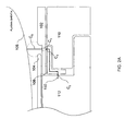
- FIG. 1 illustrates a simplified cross section view of a plasma processing chamber 100.
- a wafer 104 sits on a chuck 112 which supports the wafer in the plasma processing chamber.
- Chuck 112 acts as a work piece holder and may be electrically energized by an RF power source to facilitate etching and deposition, as is well known.
- a coupling ring 108 is shown disposed between chuck 112 and a ceramic ring 110.
- One of the functions of coupling ring 108 includes providing a current path from chuck 112 to an edge ring 102.
- Edge ring 102 performs many functions, including positioning wafer 104 on chuck 112 and shielding the underlying components not protected by the wafer itself from being damaged by the ions of the plasma.
- edge ring 112 One important function of edge ring 112 relates to its effect on process uniformity across the substrate. It is well known that the equipotential lines of the plasma sheath 106 curve upward sharply past the edge of the chuck. Without an edge ring, the substrate edge electrically defines the outer edge of the chuck, and the equipotential lines would curve upward sharply in the vicinity of the substrate edge. As such, areas of the substrate around the substrate edge would experience a different plasma environment from the plasma environment that exists at the center of substrate, thereby contributing to poor process uniformity across the substrate surface.
- the edge of the chuck appears electrically to the plasma to extend some distance outside of the edge of the substrate.
- the equipotential lines of the plasma sheath stays more constant over the entire surface of the substrate, thereby contributing to process uniformity across the substrate surface.
- edge rings tend to be worn away over time by the plasma environment. As the edge ring wears away, the plasma environment in the vicinity of the damaged regions of the edge ring changes. The change to the plasma in turn causes the process result to change over time, and contributes to process degradation as the edge ring wears away. This is the case even if the process employs the same recipe in the same chamber time after time.
- the invention relates, in one embodiment, to a method for processing a plurality of substrates in a plasma processing chamber of a plasma processing.
- a method for processing a plurality of substrates in a plasma processing chamber of a plasma processing system each of said substrates being disposed on a chuck (112) and surrounded by an edge ring (102) during said processing, said plasma processing system having a coupling ring (408) configured to provide a current path between said chuck and said edge ring, the method comprising:
- the invention in another embodiment, relates to a plasma processing system having at least one plasma processing chamber for processing a plurality of substrates.
- the invention relates to a plasma processing system having at least one plasma processing chamber for processing a plurality of substrates.
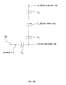
- FIG. 2A illustrates another plasma processing chamber diagram is which the capacitive path 150 from plasma sheath 106 to chuck 112 through edge ring 102 is depicted.
- plasma sheath 106, wafer 104, chuck 112, coupling ring 108, edge ring 102, and ceramic ring 110 are as shown in FIG. 1 .
- an equivalent capacitance C0 which is defined by the surface of chuck 112, the surface of coupling ring 108, and the space in between.
- edge ring 102 forms another capacitance C1.
- gap between plasma sheath 106 and the upper surface of edge ring 102 forms another capacitance Cs along capacitive path 150.
- FIG. 2B a simplified electrical diagram for capacitive path 150 is shown.
- Chuck 112 is electrically coupled in series with capacitance C0, which is shown disposed between chuck 112 and coupling ring 108.
- Capacitance C2 is coupled in series along the capacitive path 150 between coupling ring 108 and the lower face of edge ring 102.
- Capacitance C1, which is formed by the dielectric material of edge ring 102 is shown coupled in series with capacitance C2.
- Capacitance Cs completes the capacitive path 150 by coupling in series with capacitance C2 between capacitance C2 and plasma sheath 106.
- the capacitance C 1 attributable to the dielectric material of the edge ring changes.
- the change in capacitance C 1 in turn affects the plasma environment in the vicinity of the damaged regions of the edge ring. As the plasma environment changes, process result degrades.
- the edge ring would either not erode or erode at a slow rate which would allow the etcher to remain in service until some later service interval was reached.
- Some semiconductor manufacturing processes cannot tolerate the etching characteristics changing more than a very small amount, and as such the edge ring lifetime is shortened more so than by the mere loss of material. It is the purpose of this invention to effectively extend the service life of the edge ring by compensating for the erosion so as to minimize the substrate edge etch rate change and feature tilt effects with time.
- the change in the capacitance along capacitive path 150 attributable to edge ring damage is compensated for by reducing the capacitance of one or more of capacitances C0, C2 or CS.
- the increase in capacitance C1 due to edge ring thinning damage is offset by decreasing the capacitance C2 associated with the gap between the lower surface of the edge ring and the coupling ring.
- decreasing the capacitance C2 is accomplished by providing a mechanism that can move the edge ring and the coupling ring further apart to decrease the capacitance C2 in between to compensate for the increased capacitance C1 caused by edge ring thinning damage.
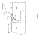
- FIG. 4A illustrates, in accordance with one embodiment of the present invention, a simplified cross section view of a plasma processing chamber with a variable position coupling ring 408.
- variable position coupling ring 408 is configured to travel along a path 404. Since the capacitance value of capacitance C2 is dependent upon the distance between lower surface of edge ring 102 and variable position coupling ring 408, changing the position of variable position edge ring 408 will change the capacitance value of capacitance C2.
- the increase in the capacitance C1 associated with damaged edge ring 102 can now be offset by changing the capacitance C2 through the repositioning of variable position coupling ring 408 along path 404.
- the net result is that the total capacitance along capacitance path 150 stays substantially the same, or is changed to a lesser extent. Since the capacitance between the plasma sheath and the chuck remains substantially unchanged or is changed to a lesser extent with the use of a variable position coupling ring, the impedance between the plasma sheath and the chuck stays substantially unchanged or is changed to a lesser extent as the edge ring wears away. This in turn helps keep the plasma environment in the vicinity of the damaged regions of the edge ring substantially unchanged or is changed to a lesser extent as the edge ring wears away.
- the use of a variable position coupling ring delays the need to change the edge ring. As the edge ring wears away, the coupling ring is repositioned to correct for process degradation. A point will still be reached at which edge ring 102 will need to be replaced because of extensive structural damage or because the increase in the capacitance C1 due to edge ring damage cannot be adequately compensated beyond some point by further decreasing one of the other capacitances. However, replacement will occur less frequently than in the prior art, thereby reducing both costly manufacturing down time as well as the need for equipment recalibration necessitated by the replacement process.
- the amount of edge ring thinning or damage may be empirically determined for a particular process in a particular plasma processing chamber by measuring the edge ring thickness over time. For example, the thickness of the edge ring in the affected regions may be measured using a contact probe, in one embodiment. Once the amount of edge ring thinning is determined as a function of time or as a function of the number of substrates processed, the capacitance value C1 as a function of time or as a function of the number of substrates processed may be determined.
- This information may be used to determine the required decrease in capacitance, as a function of time or as a function of the number of substrates processed, in one or more of the other capacitances along the capacitive path between the plasma sheath and the chuck in order to offset the increase in the capacitance caused by edge ring thinning damage.
- this information may in turn be employed to calculate the required gap during production runs between the coupling ring and the edge ring, as a function of time or as a function of the number of substrates processed, to satisfactorily offset the increase in the capacitance caused by edge ring thinning damage.
- the decrease in the capacitance value of one or more of the other capacitances along the capacitive path between the plasma sheath and the chuck may be computed, either theoretically or via computer-assisted modeling taken into account, among others, the materials of the various components of the plasma processing chamber, the geometry of the chamber and its components, and the process recipe. This information may then be employed to reduce the capacitance of one or more of the other capacitances along the capacitive path between the plasma sheath and the chuck in the production chamber.
- Reducing the capacitance value of one or more of the other capacitances along the capacitive path between the plasma sheath and the chuck through the edge ring may be accomplished in various ways.
- one or more linear or screw actuators may be provided to physically move variable position coupling ring 408 relative to the edge ring.
- the actuator(s) may be anchored against chuck 112 or ceramic ring 110 or even edge ring 102 if desired.
- the edge ring may alternately or additionally be made movable to compensate for the increase in the capacitance C1 attributable to edge ring thinning damage. Still further, it is possible to keep the coupling and edge rings stationary and provide movable inserts, which can be positioned as needed in the gaps between the chuck and the coupling ring, or in between the coupling ring and the edge ring, or in between the edge ring and the plasma sheath, to offset the increase in the capacitance C1 attributable to edge ring thinning damage.
- the capacitance adjustment be performed in-situ. That is, it is preferable that there be a mechanism provided with the plasma processing chamber to allow the capacitance of one or more of the other capacitances along the capacitive path between the plasma sheath and the chuck to be adjusted without the need to remove the plasma processing chamber from service on the production line for an extended period of time.
- the actuator coupled to the variable position coupling ring is but one example of this type of in-situ capacitance adjustment mechanism to offset the increase in the capacitance C 1 attributable to edge ring thinning damage.
- the coupling ring may be made stationary but may have a variable impedance to the chuck through the use of a variable impedance device, such as a variable capacitor.
- the adjustment may be made by adjusting the value of the variable impedance device as necessary to offset the change in the capacitance of the edge ring.
- some chamber designs may include fewer or a greater number of components in the capacitive path between the plasma sheath and the chuck through the edge ring. Irrespective of the number of components (such as rings or any other structures) involved, as long as one or more of the other capacitances along the capacitive path between the plasma sheath and the chuck body can be reduced to offset the increase in the capacitance C1 attributable to edge ring thinning damage, process degradation is reduced and the edge ring can be employed for a longer period of time before requiring a replacement.
- the amount of deposition over time may be empirically determined to ascertain the change in the capacitance of the edge ring due to the deposition, or the change in the capacitance of the edge ring may be modeled or mathematically computed. This information may then be employed to facilitate compensation by adjusting one or more capacitances along the aforementioned capacitive path.
- the invention applies to any and all plasma processing systems that experience process degradation due to edge ring thinning damage or the buildup of material on the edge ring, irrespective of how the plasma is generated, including inductively coupled plasma processing systems, capacitively coupled plasma processing systems, and others. It should also be noted that there are many alternative ways of implementing the methods and apparatuses of the present invention as defined in the following appended claims.
Landscapes
- Physics & Mathematics (AREA)
- Engineering & Computer Science (AREA)
- Plasma & Fusion (AREA)
- Chemical & Material Sciences (AREA)
- Analytical Chemistry (AREA)
- Electromagnetism (AREA)
- Spectroscopy & Molecular Physics (AREA)
- Drying Of Semiconductors (AREA)
- Plasma Technology (AREA)
- Chemical Vapour Deposition (AREA)
- Ceramic Products (AREA)
- External Artificial Organs (AREA)
Claims (15)
- Méthode de traitement d'une pluralité de substrats dans une chambre de traitement à plasma d'un système de traitement à plasma, chacun desdits substrats étant placé sur un mandrin (112) et entouré par un anneau de bord (102) pendant ledit traitement, ledit système de traitement à plasma présentant un anneau de couplage (408), configuré pour fournir un chemin à courant entre ledit mandrin et ledit anneau de bord, la méthode comprenant :- le traitement d'un premier substrat (104) de ladite pluralité de substrats selon une recette de traitement donnée, dans ladite chambre de traitement à plasma,- l'ajustage ensuite d'une valeur de capacité le long d'un chemin à capacité entre une gaine à plasma (106) dans ladite chambre de traitement à plasma et ledit mandrin en passant par l'anneau de bord, et ;- le traitement d'un deuxième substrat de ladite pluralité de substrats selon ladite recette de traitement donnée après ledit ajustage, méthode selon laquelle l'ajustage est effectué sans nécessiter de changement de l'anneau de bord, et selon laquelle ledit anneau de couplage peut être déplacé le long d'un axe perpendiculaire à une surface dudit anneau de bord, afin d'augmenter l'écart entre des surfaces adjacentes le long dudit chemin de capacité pour effectuer ledit ajustage, lesdites surfaces adjacentes incluant ladite surface dudit anneau de bord et une surface dudit anneau de couplage.
- Méthode selon la revendication 1, selon laquelle l'anneau de couplage est écarté dudit anneau de bord, afin de réduire la capacité entre ledit anneau de couplage et ledit anneau de bord.
- Méthode selon la revendication 1, selon laquelle l'ajustage comprend la réduction d'une ou plusieurs capacités premières, une capacité seconde, et une capacité tierce, ladite capacité première se situant entre ledit mandrin et ledit anneau de couplage, ladite capacité seconde se situant entre ledit anneau de couplage et ledit anneau de bord, et la capacité tierce étant formée par le matériau diélectrique dudit anneau de bord.
- Méthode selon la revendication 1, selon laquelle ledit ajustage comprend le déplacement dudit anneau de couplage le long dudit axe qui est perpendiculaire à ladite surface dudit anneau de bord afin d'augmenter ledit écart.
- Méthode selon la revendication1, selon laquelle ledit ajustage comprend le maintien en position stationnaire dudit anneau de couplage et la présence d'inserts pouvant être déplacés, ces derniers étant positionnés dans une ou plusieurs ouvertures première, seconde ou tierce, ladite ouverture première se situant entre ledit mandrin et ledit anneau de couplage, ladite ouverture seconde se situant entre ledit anneau de couplage et ledit anneau de bord, ladite ouverture tierce se situant entre ledit anneau de bord et la gaine à plasma.
- Méthode selon la revendication 1, selon laquelle ledit ajustage comprend le maintien en position stationnaire dudit anneau de couplage ou dudit anneau de bord et la présence d'inserts pouvant être déplacés entre ledit anneau de couplage et ledit anneau de bord.
- Système de traitement à plasma présentant au moins une chambre de traitement à plasma pour le traitement d'une pluralité de substrats, ladite chambre comprenant :- un mandrin (112) configuré pour soutenir un substrat (104) pendant ledit traitement;- un anneau de bord (102) présentant une périphérie extérieure, celle-ci entourant ledit mandrin, dans lequel ledit anneau de bord est configuré pour être disposé le long d'un chemin à capacité entre une gaine à plasma (106) et ledit mandrin pendant ledit traitement, ladite gaine à plasma étant associée à un plasma généré pendant ledit traitement; et- un anneau de couplage configuré pour définir un chemin à courant entre ledit mandrin et ledit anneau de bord, situé le long dudit chemin à capacité et configuré pour pouvoir être déplacé pour ajuster la capacité entre ledit anneau de couplage et ledit anneau de bord.
- Système de traitement à plasma selon la revendication 7, dans lequel ledit anneau de couplage est configuré pour pouvoir être repositionné à distance dudit anneau de bord, afin de réduire ladite capacité.
- Système de traitement à plasma selon l'une quelconque des revendications 7 ou 8, dans lequel ledit anneau de couplage est en outre configuré pour fournir un chemin à courant dudit mandrin jusque audit anneau de bord.
- Système de traitement à plasma selon l'une quelconque des revendications 7 à 9, lequel comprend en outre un ou plusieurs actionneurs ancrés à un anneau céramique.
- Système de traitement à plasma selon l'une quelconque des revendications 7 à 10, dans lequel comprend en outre un dispositif à impédance variable, afin de combler un changement de capacité dudit anneau de bord pour le cas où ledit anneau de couplage est rendu stationnaire.
- Système de traitement à plasma, présentant au moins une chambre de traitement à plasma pour le traitement d'une pluralité de substrats, ladite chambre comprenant :- un mandrin (112) configuré pour soutenir un substrat (104) pendant ledit traitement;- un anneau de bord (102) présentant une périphérie extérieure, celle-ci entourant ledit mandrin, dans lequel ledit anneau de bord est configuré pour être disposé le long d'un chemin à capacité entre une gaine à plasma (106) et ledit mandrin pendant ledit traitement, ladite gaine à plasma étant associée à un plasma généré pendant ledit traitement;- un anneau de couplage configuré pour définir un chemin à courant entre ledit mandrin et ledit anneau de bord, situé le long dudit chemin à capacité et rendu stationnaire; et- des inserts pouvant être déplacés, situés dans des ouverture première, seconde, et tierce, ladite ouverture première se situant entre ledit mandrin et ledit anneau de couplage, ladite ouverture seconde se situant entre ledit anneau de couplage et ledit anneau de bord, et ladite ouverture tierce se situant entre ledit anneau de bord et ladite gaine à plasma, lesdits inserts pouvant être déplacés étant configurés pour ajuster la capacité associée à une ou plusieurs des ouvertures première, seconde, et tierce.
- Système de traitement à plasma selon la revendication 12, lequel comprend en outre un actionneur couplé audit anneau de couplage pour l'ajustage in situ de la capacité.
- Système de traitement à plasma selon l'une quelconque des revendications 12 ou 13, lequel comprend en outre un dispositif à impédance variable pour fournir une impédance variable dudit anneau de couplage audit mandrin.
- Système de traitement à plasma selon l'une quelconque des revendications 12, 13 ou 14, dans lequel les inserts pouvant être déplacés sont positionnés dans lesdites ouvertures première ou seconde.
Applications Claiming Priority (3)
| Application Number | Priority Date | Filing Date | Title |
|---|---|---|---|
| US247812 | 1994-05-23 | ||
| US10/247,812 US6896765B2 (en) | 2002-09-18 | 2002-09-18 | Method and apparatus for the compensation of edge ring wear in a plasma processing chamber |
| PCT/US2003/029309 WO2004027816A2 (fr) | 2002-09-18 | 2003-09-16 | Procede et appareil pour compenser l'usure d'un anneau de bordure dans une chambre de traitement au plasma |
Publications (2)
| Publication Number | Publication Date |
|---|---|
| EP1540695A2 EP1540695A2 (fr) | 2005-06-15 |
| EP1540695B1 true EP1540695B1 (fr) | 2010-03-03 |
Family
ID=31992568
Family Applications (1)
| Application Number | Title | Priority Date | Filing Date |
|---|---|---|---|
| EP03797912A Expired - Lifetime EP1540695B1 (fr) | 2002-09-18 | 2003-09-16 | Procede et appareil pour compenser l'usure d'un anneau de bordure dans une chambre de traitement au plasma |
Country Status (11)
| Country | Link |
|---|---|
| US (2) | US6896765B2 (fr) |
| EP (1) | EP1540695B1 (fr) |
| JP (1) | JP4841840B2 (fr) |
| KR (1) | KR101075048B1 (fr) |
| CN (1) | CN100481307C (fr) |
| AT (1) | ATE459975T1 (fr) |
| AU (1) | AU2003276895A1 (fr) |
| DE (1) | DE60331557D1 (fr) |
| IL (1) | IL167491A (fr) |
| TW (1) | TWI324809B (fr) |
| WO (1) | WO2004027816A2 (fr) |
Cited By (1)
| Publication number | Priority date | Publication date | Assignee | Title |
|---|---|---|---|---|
| US10854492B2 (en) | 2015-08-18 | 2020-12-01 | Lam Research Corporation | Edge ring assembly for improving feature profile tilting at extreme edge of wafer |
Families Citing this family (95)
| Publication number | Priority date | Publication date | Assignee | Title |
|---|---|---|---|---|
| KR100657054B1 (ko) * | 2003-01-07 | 2006-12-13 | 동경 엘렉트론 주식회사 | 플라즈마 처리 장치 및 포커스 링 |
| US7658816B2 (en) * | 2003-09-05 | 2010-02-09 | Tokyo Electron Limited | Focus ring and plasma processing apparatus |
| US7244336B2 (en) * | 2003-12-17 | 2007-07-17 | Lam Research Corporation | Temperature controlled hot edge ring assembly for reducing plasma reactor etch rate drift |
| KR100610010B1 (ko) * | 2004-07-20 | 2006-08-08 | 삼성전자주식회사 | 반도체 식각 장치 |
| JP4566789B2 (ja) * | 2005-03-07 | 2010-10-20 | 株式会社日立ハイテクノロジーズ | プラズマ処理方法およびプラズマ処理装置 |
| JP2007250967A (ja) * | 2006-03-17 | 2007-09-27 | Tokyo Electron Ltd | プラズマ処理装置および方法とフォーカスリング |
| JP5069452B2 (ja) * | 2006-04-27 | 2012-11-07 | アプライド マテリアルズ インコーポレイテッド | 二重温度帯を有する静電チャックをもつ基板支持体 |
| US7572737B1 (en) * | 2006-06-30 | 2009-08-11 | Lam Research Corporation | Apparatus and methods for adjusting an edge ring potential substrate processing |
| US7943007B2 (en) | 2007-01-26 | 2011-05-17 | Lam Research Corporation | Configurable bevel etcher |
| JP5317424B2 (ja) * | 2007-03-28 | 2013-10-16 | 東京エレクトロン株式会社 | プラズマ処理装置 |
| JP4988402B2 (ja) * | 2007-03-30 | 2012-08-01 | 株式会社日立ハイテクノロジーズ | プラズマ処理装置 |
| US7837827B2 (en) * | 2007-06-28 | 2010-11-23 | Lam Research Corporation | Edge ring arrangements for substrate processing |
| US8563619B2 (en) * | 2007-06-28 | 2013-10-22 | Lam Research Corporation | Methods and arrangements for plasma processing system with tunable capacitance |
| US20090025636A1 (en) * | 2007-07-27 | 2009-01-29 | Applied Materials, Inc. | High profile minimum contact process kit for hdp-cvd application |
| US8343305B2 (en) | 2007-09-04 | 2013-01-01 | Lam Research Corporation | Method and apparatus for diagnosing status of parts in real time in plasma processing equipment |
| CN101552182B (zh) * | 2008-03-31 | 2010-11-03 | 北京北方微电子基地设备工艺研究中心有限责任公司 | 一种用于半导体制造工艺中的边缘环机构 |
| US20090261065A1 (en) * | 2008-04-18 | 2009-10-22 | Lam Research Corporation | Components for use in a plasma chamber having reduced particle generation and method of making |
| KR101624123B1 (ko) * | 2008-10-31 | 2016-05-25 | 램 리써치 코포레이션 | 플라즈마 프로세싱 챔버의 하부 전극 어셈블리 |
| WO2010101191A1 (fr) * | 2009-03-03 | 2010-09-10 | 東京エレクトロン株式会社 | Structure de table de placement, appareil de formation de film et procédé de récupération de matière première |
| JP5350043B2 (ja) * | 2009-03-31 | 2013-11-27 | 東京エレクトロン株式会社 | プラズマ処理装置及びプラズマ処理方法 |
| US20110011534A1 (en) * | 2009-07-17 | 2011-01-20 | Rajinder Dhindsa | Apparatus for adjusting an edge ring potential during substrate processing |
| SG170717A1 (en) * | 2009-11-02 | 2011-05-30 | Lam Res Corp | Hot edge ring with sloped upper surface |
| JP5808750B2 (ja) * | 2009-11-30 | 2015-11-10 | ラム リサーチ コーポレーションLam Research Corporation | 傾斜側壁を備える静電チャック |
| JP5654297B2 (ja) * | 2010-09-14 | 2015-01-14 | 東京エレクトロン株式会社 | プラズマ処理装置及びプラズマ処理方法 |
| JP5741124B2 (ja) * | 2011-03-29 | 2015-07-01 | 東京エレクトロン株式会社 | プラズマ処理装置 |
| CN103177925B (zh) * | 2011-12-23 | 2015-08-26 | 中微半导体设备(上海)有限公司 | 一种用于等离子体处理装置的可调节约束环 |
| CN103187234B (zh) * | 2011-12-30 | 2016-03-16 | 中微半导体设备(上海)有限公司 | 一种用于等离子体处理装置的可调节约束装置 |
| US8525069B1 (en) * | 2012-05-18 | 2013-09-03 | Hypertherm, Inc. | Method and apparatus for improved cutting life of a plasma arc torch |
| US20140034242A1 (en) * | 2012-07-31 | 2014-02-06 | Lam Research Corporation | Edge ring assembly for plasma processing chamber and method of manufacture thereof |
| US10002744B2 (en) * | 2013-12-17 | 2018-06-19 | Tokyo Electron Limited | System and method for controlling plasma density |
| US10804081B2 (en) | 2013-12-20 | 2020-10-13 | Lam Research Corporation | Edge ring dimensioned to extend lifetime of elastomer seal in a plasma processing chamber |
| JP5767373B2 (ja) * | 2014-07-29 | 2015-08-19 | 東京エレクトロン株式会社 | プラズマ処理装置及びプラズマ処理方法並びにこれを実施するためのプログラムを記憶する記憶媒体 |
| US9873180B2 (en) | 2014-10-17 | 2018-01-23 | Applied Materials, Inc. | CMP pad construction with composite material properties using additive manufacturing processes |
| US11745302B2 (en) | 2014-10-17 | 2023-09-05 | Applied Materials, Inc. | Methods and precursor formulations for forming advanced polishing pads by use of an additive manufacturing process |
| US10875153B2 (en) | 2014-10-17 | 2020-12-29 | Applied Materials, Inc. | Advanced polishing pad materials and formulations |
| US9776361B2 (en) | 2014-10-17 | 2017-10-03 | Applied Materials, Inc. | Polishing articles and integrated system and methods for manufacturing chemical mechanical polishing articles |
| SG11201703114QA (en) | 2014-10-17 | 2017-06-29 | Applied Materials Inc | Cmp pad construction with composite material properties using additive manufacturing processes |
| US11605546B2 (en) * | 2015-01-16 | 2023-03-14 | Lam Research Corporation | Moveable edge coupling ring for edge process control during semiconductor wafer processing |
| US10658222B2 (en) * | 2015-01-16 | 2020-05-19 | Lam Research Corporation | Moveable edge coupling ring for edge process control during semiconductor wafer processing |
| US10957561B2 (en) | 2015-07-30 | 2021-03-23 | Lam Research Corporation | Gas delivery system |
| CN105185732A (zh) * | 2015-08-24 | 2015-12-23 | 沈阳拓荆科技有限公司 | 一种可改变晶圆表面薄膜形貌的陶瓷环 |
| US10593574B2 (en) | 2015-11-06 | 2020-03-17 | Applied Materials, Inc. | Techniques for combining CMP process tracking data with 3D printed CMP consumables |
| US10825659B2 (en) | 2016-01-07 | 2020-11-03 | Lam Research Corporation | Substrate processing chamber including multiple gas injection points and dual injector |
| US10391605B2 (en) | 2016-01-19 | 2019-08-27 | Applied Materials, Inc. | Method and apparatus for forming porous advanced polishing pads using an additive manufacturing process |
| US10685862B2 (en) | 2016-01-22 | 2020-06-16 | Applied Materials, Inc. | Controlling the RF amplitude of an edge ring of a capacitively coupled plasma process device |
| JP6888007B2 (ja) | 2016-01-26 | 2021-06-16 | アプライド マテリアルズ インコーポレイテッドApplied Materials,Incorporated | ウェハエッジリングの持ち上げに関する解決 |
| CN108369922B (zh) | 2016-01-26 | 2023-03-21 | 应用材料公司 | 晶片边缘环升降解决方案 |
| US10699878B2 (en) | 2016-02-12 | 2020-06-30 | Lam Research Corporation | Chamber member of a plasma source and pedestal with radially outward positioned lift pins for translation of a substrate c-ring |
| US10651015B2 (en) | 2016-02-12 | 2020-05-12 | Lam Research Corporation | Variable depth edge ring for etch uniformity control |
| US10438833B2 (en) | 2016-02-16 | 2019-10-08 | Lam Research Corporation | Wafer lift ring system for wafer transfer |
| US11011353B2 (en) | 2016-03-29 | 2021-05-18 | Lam Research Corporation | Systems and methods for performing edge ring characterization |
| US10312121B2 (en) * | 2016-03-29 | 2019-06-04 | Lam Research Corporation | Systems and methods for aligning measurement device in substrate processing systems |
| US9852889B1 (en) * | 2016-06-22 | 2017-12-26 | Lam Research Corporation | Systems and methods for controlling directionality of ions in an edge region by using an electrode within a coupling ring |
| JP2018006299A (ja) | 2016-07-08 | 2018-01-11 | 東芝メモリ株式会社 | プラズマ処理装置用処理対象支持台、プラズマ処理装置及びプラズマ処理方法 |
| CN107644802B (zh) * | 2016-07-21 | 2019-09-06 | 中微半导体设备(上海)股份有限公司 | 等离子体刻蚀装置及其边缘环组件与静电夹盘 |
| US10410832B2 (en) | 2016-08-19 | 2019-09-10 | Lam Research Corporation | Control of on-wafer CD uniformity with movable edge ring and gas injection adjustment |
| US9947517B1 (en) | 2016-12-16 | 2018-04-17 | Applied Materials, Inc. | Adjustable extended electrode for edge uniformity control |
| KR102581226B1 (ko) | 2016-12-23 | 2023-09-20 | 삼성전자주식회사 | 플라즈마 처리 장치 |
| US10553404B2 (en) | 2017-02-01 | 2020-02-04 | Applied Materials, Inc. | Adjustable extended electrode for edge uniformity control |
| US11471999B2 (en) | 2017-07-26 | 2022-10-18 | Applied Materials, Inc. | Integrated abrasive polishing pads and manufacturing methods |
| JP6974088B2 (ja) * | 2017-09-15 | 2021-12-01 | 東京エレクトロン株式会社 | プラズマ処理装置及びプラズマ処理方法 |
| US11075105B2 (en) | 2017-09-21 | 2021-07-27 | Applied Materials, Inc. | In-situ apparatus for semiconductor process module |
| CN118380372A (zh) | 2017-11-21 | 2024-07-23 | 朗姆研究公司 | 底部边缘环和中部边缘环 |
| CN109920716B (zh) * | 2017-12-13 | 2021-06-08 | 中微半导体设备(上海)股份有限公司 | 一种均衡刻蚀速率的等离子体处理装置及方法 |
| CN115938902B (zh) * | 2017-12-15 | 2024-10-29 | 朗姆研究公司 | 等离子体室中使用的环形结构和系统 |
| US11043400B2 (en) | 2017-12-21 | 2021-06-22 | Applied Materials, Inc. | Movable and removable process kit |
| JP7055040B2 (ja) * | 2018-03-07 | 2022-04-15 | 東京エレクトロン株式会社 | 被処理体の載置装置及び処理装置 |
| KR101995760B1 (ko) * | 2018-04-02 | 2019-07-03 | 세메스 주식회사 | 기판 처리 장치 및 기판 처리 방법 |
| US11201037B2 (en) | 2018-05-28 | 2021-12-14 | Applied Materials, Inc. | Process kit with adjustable tuning ring for edge uniformity control |
| US11935773B2 (en) | 2018-06-14 | 2024-03-19 | Applied Materials, Inc. | Calibration jig and calibration method |
| CN118398464A (zh) | 2018-08-13 | 2024-07-26 | 朗姆研究公司 | 可更换和/或可折叠的用于等离子鞘调整的并入边缘环定位和定心功能的边缘环组件 |
| KR20210042171A (ko) | 2018-09-04 | 2021-04-16 | 어플라이드 머티어리얼스, 인코포레이티드 | 진보한 폴리싱 패드들을 위한 제형들 |
| US11289310B2 (en) | 2018-11-21 | 2022-03-29 | Applied Materials, Inc. | Circuits for edge ring control in shaped DC pulsed plasma process device |
| US11512393B2 (en) * | 2018-11-29 | 2022-11-29 | Lam Research Corporation | Dynamic sheath control with edge ring lift |
| US10903050B2 (en) * | 2018-12-10 | 2021-01-26 | Lam Research Corporation | Endpoint sensor based control including adjustment of an edge ring parameter for each substrate processed to maintain etch rate uniformity |
| US11955314B2 (en) * | 2019-01-09 | 2024-04-09 | Tokyo Electron Limited | Plasma processing apparatus |
| WO2020214327A1 (fr) | 2019-04-19 | 2020-10-22 | Applied Materials, Inc. | Retrait d'anneau d'une chambre de traitement |
| US12009236B2 (en) | 2019-04-22 | 2024-06-11 | Applied Materials, Inc. | Sensors and system for in-situ edge ring erosion monitor |
| KR102214333B1 (ko) | 2019-06-27 | 2021-02-10 | 세메스 주식회사 | 기판 처리 장치 및 기판 처리 방법 |
| JP7278160B2 (ja) * | 2019-07-01 | 2023-05-19 | 東京エレクトロン株式会社 | エッチング方法及びプラズマ処理装置 |
| CN118431063A (zh) * | 2019-08-05 | 2024-08-02 | 朗姆研究公司 | 用于衬底处理系统的边缘环系统 |
| CN112885690B (zh) * | 2019-11-29 | 2023-10-20 | 中微半导体设备(上海)股份有限公司 | 一种等离子体处理装置 |
| KR102905595B1 (ko) | 2020-03-23 | 2025-12-29 | 램 리써치 코포레이션 | 기판 프로세싱 시스템들에서의 중간-링 부식 보상 |
| US11380575B2 (en) | 2020-07-27 | 2022-07-05 | Applied Materials, Inc. | Film thickness uniformity improvement using edge ring and bias electrode geometry |
| USD1034491S1 (en) | 2020-07-27 | 2024-07-09 | Applied Materials, Inc. | Edge ring |
| WO2022076227A1 (fr) * | 2020-10-05 | 2022-04-14 | Lam Research Corporation | Bagues de bord mobile pour systèmes de traitement de plasma |
| CN112259452B (zh) * | 2020-10-21 | 2023-04-07 | 上海华力集成电路制造有限公司 | 等离子体干法刻蚀工艺的控制方法 |
| KR102587757B1 (ko) | 2021-01-20 | 2023-10-12 | 주식회사 레인테크 | 부착장치 및 부착방법 |
| KR102335630B1 (ko) | 2021-04-20 | 2021-12-08 | (주)앤피에스 | 열원 장치, 기판 지지 장치 및 기판 처리 설비 |
| KR102911513B1 (ko) | 2021-08-17 | 2026-01-12 | 도쿄엘렉트론가부시키가이샤 | 반도체 플라즈마 공정 챔버 내의 소모성 부품의 특성을 측정하기 위한 광센서 |
| JP7648498B2 (ja) * | 2021-10-07 | 2025-03-18 | 東京エレクトロン株式会社 | 制御プログラム、制御方法、及びプラズマ処理装置 |
| KR102896325B1 (ko) | 2021-11-09 | 2025-12-08 | 삼성전자주식회사 | 척 어셈블리, 그를 포함하는 반도체 소자의 제조 장치, 및 반도체 소자의 제조방법 |
| JP7391283B2 (ja) * | 2021-11-18 | 2023-12-04 | 東京エレクトロン株式会社 | 基板保持方法及び基板処理装置 |
| US12488965B2 (en) * | 2022-04-27 | 2025-12-02 | Taiwan Semiconductor Manufacturing Company, Ltd. | Device and method for treating substrate |
| KR102895540B1 (ko) | 2022-07-29 | 2025-12-03 | 세메스 주식회사 | 가변 커패시턴스 장치, 이를 포함하는 기판 처리 장치 및 기판 처리 방법 |
Family Cites Families (12)
| Publication number | Priority date | Publication date | Assignee | Title |
|---|---|---|---|---|
| JPH04110653A (ja) * | 1990-08-31 | 1992-04-13 | Hitachi Ltd | プラズマを用いた気体試料の分析方法 |
| TW418461B (en) * | 1997-03-07 | 2001-01-11 | Tokyo Electron Ltd | Plasma etching device |
| US6074488A (en) * | 1997-09-16 | 2000-06-13 | Applied Materials, Inc | Plasma chamber support having an electrically coupled collar ring |
| US6039836A (en) | 1997-12-19 | 2000-03-21 | Lam Research Corporation | Focus rings |
| US6013984A (en) * | 1998-06-10 | 2000-01-11 | Lam Research Corporation | Ion energy attenuation method by determining the required number of ion collisions |
| US6363882B1 (en) * | 1999-12-30 | 2002-04-02 | Lam Research Corporation | Lower electrode design for higher uniformity |
| US6383931B1 (en) * | 2000-02-11 | 2002-05-07 | Lam Research Corporation | Convertible hot edge ring to improve low-K dielectric etch |
| US6528751B1 (en) * | 2000-03-17 | 2003-03-04 | Applied Materials, Inc. | Plasma reactor with overhead RF electrode tuned to the plasma |
| TW506234B (en) * | 2000-09-18 | 2002-10-11 | Tokyo Electron Ltd | Tunable focus ring for plasma processing |
| US6475336B1 (en) * | 2000-10-06 | 2002-11-05 | Lam Research Corporation | Electrostatically clamped edge ring for plasma processing |
| US6391787B1 (en) * | 2000-10-13 | 2002-05-21 | Lam Research Corporation | Stepped upper electrode for plasma processing uniformity |
| JP3388228B2 (ja) * | 2000-12-07 | 2003-03-17 | 株式会社半導体先端テクノロジーズ | プラズマエッチング装置、及びプラズマエッチング方法 |
-
2002
- 2002-09-18 US US10/247,812 patent/US6896765B2/en not_active Expired - Lifetime
-
2003
- 2003-09-16 EP EP03797912A patent/EP1540695B1/fr not_active Expired - Lifetime
- 2003-09-16 AT AT03797912T patent/ATE459975T1/de not_active IP Right Cessation
- 2003-09-16 WO PCT/US2003/029309 patent/WO2004027816A2/fr not_active Ceased
- 2003-09-16 CN CNB038223147A patent/CN100481307C/zh not_active Expired - Lifetime
- 2003-09-16 JP JP2004537951A patent/JP4841840B2/ja not_active Expired - Lifetime
- 2003-09-16 KR KR1020057004768A patent/KR101075048B1/ko not_active Expired - Lifetime
- 2003-09-16 DE DE60331557T patent/DE60331557D1/de not_active Expired - Lifetime
- 2003-09-16 AU AU2003276895A patent/AU2003276895A1/en not_active Abandoned
- 2003-09-18 TW TW092125775A patent/TWI324809B/zh not_active IP Right Cessation
-
2004
- 2004-10-22 US US10/971,971 patent/US7176403B2/en not_active Expired - Lifetime
-
2005
- 2005-03-16 IL IL167491A patent/IL167491A/en not_active IP Right Cessation
Cited By (1)
| Publication number | Priority date | Publication date | Assignee | Title |
|---|---|---|---|---|
| US10854492B2 (en) | 2015-08-18 | 2020-12-01 | Lam Research Corporation | Edge ring assembly for improving feature profile tilting at extreme edge of wafer |
Also Published As
| Publication number | Publication date |
|---|---|
| KR101075048B1 (ko) | 2011-10-19 |
| KR20050050660A (ko) | 2005-05-31 |
| JP4841840B2 (ja) | 2011-12-21 |
| US20050056622A1 (en) | 2005-03-17 |
| IL167491A (en) | 2009-08-03 |
| US6896765B2 (en) | 2005-05-24 |
| WO2004027816A3 (fr) | 2004-12-09 |
| DE60331557D1 (de) | 2010-04-15 |
| TW200408043A (en) | 2004-05-16 |
| US7176403B2 (en) | 2007-02-13 |
| US20040053428A1 (en) | 2004-03-18 |
| AU2003276895A1 (en) | 2004-04-08 |
| WO2004027816A2 (fr) | 2004-04-01 |
| TWI324809B (en) | 2010-05-11 |
| CN1682344A (zh) | 2005-10-12 |
| CN100481307C (zh) | 2009-04-22 |
| EP1540695A2 (fr) | 2005-06-15 |
| JP2005539397A (ja) | 2005-12-22 |
| ATE459975T1 (de) | 2010-03-15 |
Similar Documents
| Publication | Publication Date | Title |
|---|---|---|
| EP1540695B1 (fr) | Procede et appareil pour compenser l'usure d'un anneau de bordure dans une chambre de traitement au plasma | |
| KR102496625B1 (ko) | 베벨 에처용 튜닝가능한 상부 플라즈마―배제―존 링 | |
| KR102721101B1 (ko) | 용량 결합형 플라즈마 처리 장치의 에지 링의 rf 진폭 제어 | |
| EP1362362B1 (fr) | Contrôle de pression sur la zone au-dessus d'une plaquette | |
| KR100938635B1 (ko) | 반경 방향 플라즈마 분포에 대한 개선된 자기 제어를 위한플라즈마 제한 배플 및 유동비 이퀄라이저 | |
| KR100900585B1 (ko) | 포커스링 및 플라즈마 처리 장치 | |
| TW201719709A (zh) | 用以改良晶圓之極限邊緣處的特徵部輪廓偏斜之邊緣環組件 | |
| US20080289766A1 (en) | Hot edge ring apparatus and method for increased etch rate uniformity and reduced polymer buildup | |
| KR20020041340A (ko) | 에칭율의 균일성을 개선하기 위한 기술 | |
| JP5305287B2 (ja) | 半導体製造装置 | |
| JP7801860B2 (ja) | 装置および方法 | |
| US6077353A (en) | Pedestal insulator for a pre-clean chamber | |
| WO2024263295A1 (fr) | Inclinaison de bague de bord réglable pour compensation d'obliquité de bord de tranche | |
| JP2000226649A (ja) | 高周波スパッタリング装置、その基板側及びターゲット側グランドリング、並びに、酸化絶縁膜の成膜方法 |
Legal Events
| Date | Code | Title | Description |
|---|---|---|---|
| PUAI | Public reference made under article 153(3) epc to a published international application that has entered the european phase |
Free format text: ORIGINAL CODE: 0009012 |
|
| 17P | Request for examination filed |
Effective date: 20050309 |
|
| AK | Designated contracting states |
Kind code of ref document: A2 Designated state(s): AT BE BG CH CY CZ DE DK EE ES FI FR GB GR HU IE IT LI LU MC NL PT RO SE SI SK TR |
|
| AX | Request for extension of the european patent |
Extension state: AL LT LV MK |
|
| DAX | Request for extension of the european patent (deleted) | ||
| 17Q | First examination report despatched |
Effective date: 20080730 |
|
| GRAP | Despatch of communication of intention to grant a patent |
Free format text: ORIGINAL CODE: EPIDOSNIGR1 |
|
| GRAS | Grant fee paid |
Free format text: ORIGINAL CODE: EPIDOSNIGR3 |
|
| GRAA | (expected) grant |
Free format text: ORIGINAL CODE: 0009210 |
|
| AK | Designated contracting states |
Kind code of ref document: B1 Designated state(s): AT BE BG CH CY CZ DE DK EE ES FI FR GB GR HU IE IT LI LU MC NL PT RO SE SI SK TR |
|
| REG | Reference to a national code |
Ref country code: GB Ref legal event code: FG4D |
|
| REG | Reference to a national code |
Ref country code: CH Ref legal event code: EP |
|
| REG | Reference to a national code |
Ref country code: IE Ref legal event code: FG4D |
|
| REF | Corresponds to: |
Ref document number: 60331557 Country of ref document: DE Date of ref document: 20100415 Kind code of ref document: P |
|
| REG | Reference to a national code |
Ref country code: NL Ref legal event code: VDEP Effective date: 20100303 |
|
| PG25 | Lapsed in a contracting state [announced via postgrant information from national office to epo] |
Ref country code: SI Free format text: LAPSE BECAUSE OF FAILURE TO SUBMIT A TRANSLATION OF THE DESCRIPTION OR TO PAY THE FEE WITHIN THE PRESCRIBED TIME-LIMIT Effective date: 20100303 Ref country code: FI Free format text: LAPSE BECAUSE OF FAILURE TO SUBMIT A TRANSLATION OF THE DESCRIPTION OR TO PAY THE FEE WITHIN THE PRESCRIBED TIME-LIMIT Effective date: 20100303 Ref country code: AT Free format text: LAPSE BECAUSE OF FAILURE TO SUBMIT A TRANSLATION OF THE DESCRIPTION OR TO PAY THE FEE WITHIN THE PRESCRIBED TIME-LIMIT Effective date: 20100303 |
|
| PG25 | Lapsed in a contracting state [announced via postgrant information from national office to epo] |
Ref country code: GR Free format text: LAPSE BECAUSE OF FAILURE TO SUBMIT A TRANSLATION OF THE DESCRIPTION OR TO PAY THE FEE WITHIN THE PRESCRIBED TIME-LIMIT Effective date: 20100604 Ref country code: BE Free format text: LAPSE BECAUSE OF FAILURE TO SUBMIT A TRANSLATION OF THE DESCRIPTION OR TO PAY THE FEE WITHIN THE PRESCRIBED TIME-LIMIT Effective date: 20100303 Ref country code: SE Free format text: LAPSE BECAUSE OF FAILURE TO SUBMIT A TRANSLATION OF THE DESCRIPTION OR TO PAY THE FEE WITHIN THE PRESCRIBED TIME-LIMIT Effective date: 20100303 Ref country code: CY Free format text: LAPSE BECAUSE OF FAILURE TO SUBMIT A TRANSLATION OF THE DESCRIPTION OR TO PAY THE FEE WITHIN THE PRESCRIBED TIME-LIMIT Effective date: 20100303 Ref country code: EE Free format text: LAPSE BECAUSE OF FAILURE TO SUBMIT A TRANSLATION OF THE DESCRIPTION OR TO PAY THE FEE WITHIN THE PRESCRIBED TIME-LIMIT Effective date: 20100303 Ref country code: ES Free format text: LAPSE BECAUSE OF FAILURE TO SUBMIT A TRANSLATION OF THE DESCRIPTION OR TO PAY THE FEE WITHIN THE PRESCRIBED TIME-LIMIT Effective date: 20100614 Ref country code: NL Free format text: LAPSE BECAUSE OF FAILURE TO SUBMIT A TRANSLATION OF THE DESCRIPTION OR TO PAY THE FEE WITHIN THE PRESCRIBED TIME-LIMIT Effective date: 20100303 Ref country code: RO Free format text: LAPSE BECAUSE OF FAILURE TO SUBMIT A TRANSLATION OF THE DESCRIPTION OR TO PAY THE FEE WITHIN THE PRESCRIBED TIME-LIMIT Effective date: 20100303 |
|
| PG25 | Lapsed in a contracting state [announced via postgrant information from national office to epo] |
Ref country code: SK Free format text: LAPSE BECAUSE OF FAILURE TO SUBMIT A TRANSLATION OF THE DESCRIPTION OR TO PAY THE FEE WITHIN THE PRESCRIBED TIME-LIMIT Effective date: 20100303 Ref country code: BG Free format text: LAPSE BECAUSE OF FAILURE TO SUBMIT A TRANSLATION OF THE DESCRIPTION OR TO PAY THE FEE WITHIN THE PRESCRIBED TIME-LIMIT Effective date: 20100603 Ref country code: CZ Free format text: LAPSE BECAUSE OF FAILURE TO SUBMIT A TRANSLATION OF THE DESCRIPTION OR TO PAY THE FEE WITHIN THE PRESCRIBED TIME-LIMIT Effective date: 20100303 |
|
| PLBE | No opposition filed within time limit |
Free format text: ORIGINAL CODE: 0009261 |
|
| STAA | Information on the status of an ep patent application or granted ep patent |
Free format text: STATUS: NO OPPOSITION FILED WITHIN TIME LIMIT |
|
| PG25 | Lapsed in a contracting state [announced via postgrant information from national office to epo] |
Ref country code: DK Free format text: LAPSE BECAUSE OF FAILURE TO SUBMIT A TRANSLATION OF THE DESCRIPTION OR TO PAY THE FEE WITHIN THE PRESCRIBED TIME-LIMIT Effective date: 20100303 Ref country code: PT Free format text: LAPSE BECAUSE OF FAILURE TO SUBMIT A TRANSLATION OF THE DESCRIPTION OR TO PAY THE FEE WITHIN THE PRESCRIBED TIME-LIMIT Effective date: 20100705 |
|
| 26N | No opposition filed |
Effective date: 20101206 |
|
| PG25 | Lapsed in a contracting state [announced via postgrant information from national office to epo] |
Ref country code: IT Free format text: LAPSE BECAUSE OF FAILURE TO SUBMIT A TRANSLATION OF THE DESCRIPTION OR TO PAY THE FEE WITHIN THE PRESCRIBED TIME-LIMIT Effective date: 20100303 |
|
| PG25 | Lapsed in a contracting state [announced via postgrant information from national office to epo] |
Ref country code: MC Free format text: LAPSE BECAUSE OF NON-PAYMENT OF DUE FEES Effective date: 20100930 |
|
| REG | Reference to a national code |
Ref country code: CH Ref legal event code: PL |
|
| PG25 | Lapsed in a contracting state [announced via postgrant information from national office to epo] |
Ref country code: CH Free format text: LAPSE BECAUSE OF NON-PAYMENT OF DUE FEES Effective date: 20100930 Ref country code: LI Free format text: LAPSE BECAUSE OF NON-PAYMENT OF DUE FEES Effective date: 20100930 |
|
| PG25 | Lapsed in a contracting state [announced via postgrant information from national office to epo] |
Ref country code: HU Free format text: LAPSE BECAUSE OF FAILURE TO SUBMIT A TRANSLATION OF THE DESCRIPTION OR TO PAY THE FEE WITHIN THE PRESCRIBED TIME-LIMIT Effective date: 20100904 Ref country code: LU Free format text: LAPSE BECAUSE OF NON-PAYMENT OF DUE FEES Effective date: 20100916 |
|
| PG25 | Lapsed in a contracting state [announced via postgrant information from national office to epo] |
Ref country code: TR Free format text: LAPSE BECAUSE OF FAILURE TO SUBMIT A TRANSLATION OF THE DESCRIPTION OR TO PAY THE FEE WITHIN THE PRESCRIBED TIME-LIMIT Effective date: 20100303 |
|
| PGFP | Annual fee paid to national office [announced via postgrant information from national office to epo] |
Ref country code: IE Payment date: 20120925 Year of fee payment: 10 Ref country code: GB Payment date: 20120925 Year of fee payment: 10 |
|
| GBPC | Gb: european patent ceased through non-payment of renewal fee |
Effective date: 20130916 |
|
| REG | Reference to a national code |
Ref country code: IE Ref legal event code: MM4A |
|
| PG25 | Lapsed in a contracting state [announced via postgrant information from national office to epo] |
Ref country code: IE Free format text: LAPSE BECAUSE OF NON-PAYMENT OF DUE FEES Effective date: 20130916 Ref country code: GB Free format text: LAPSE BECAUSE OF NON-PAYMENT OF DUE FEES Effective date: 20130916 |
|
| REG | Reference to a national code |
Ref country code: FR Ref legal event code: PLFP Year of fee payment: 13 |
|
| REG | Reference to a national code |
Ref country code: FR Ref legal event code: PLFP Year of fee payment: 14 |
|
| REG | Reference to a national code |
Ref country code: FR Ref legal event code: PLFP Year of fee payment: 15 |
|
| REG | Reference to a national code |
Ref country code: FR Ref legal event code: PLFP Year of fee payment: 16 |
|
| PGFP | Annual fee paid to national office [announced via postgrant information from national office to epo] |
Ref country code: DE Payment date: 20220928 Year of fee payment: 20 |
|
| PGFP | Annual fee paid to national office [announced via postgrant information from national office to epo] |
Ref country code: FR Payment date: 20220926 Year of fee payment: 20 |
|
| REG | Reference to a national code |
Ref country code: DE Ref legal event code: R071 Ref document number: 60331557 Country of ref document: DE |
|
| P01 | Opt-out of the competence of the unified patent court (upc) registered |
Effective date: 20231021 |