EP1540674B1 - Transformator und transformatoranordnung mit solchem transformator - Google Patents
Transformator und transformatoranordnung mit solchem transformator Download PDFInfo
- Publication number
- EP1540674B1 EP1540674B1 EP03755678A EP03755678A EP1540674B1 EP 1540674 B1 EP1540674 B1 EP 1540674B1 EP 03755678 A EP03755678 A EP 03755678A EP 03755678 A EP03755678 A EP 03755678A EP 1540674 B1 EP1540674 B1 EP 1540674B1
- Authority
- EP
- European Patent Office
- Prior art keywords
- transformer
- component
- bobbin
- voltage
- winding
- Prior art date
- Legal status (The legal status is an assumption and is not a legal conclusion. Google has not performed a legal analysis and makes no representation as to the accuracy of the status listed.)
- Expired - Lifetime
Links
Images








Classifications
-
- H—ELECTRICITY
- H05—ELECTRIC TECHNIQUES NOT OTHERWISE PROVIDED FOR
- H05B—ELECTRIC HEATING; ELECTRIC LIGHT SOURCES NOT OTHERWISE PROVIDED FOR; CIRCUIT ARRANGEMENTS FOR ELECTRIC LIGHT SOURCES, IN GENERAL
- H05B6/00—Heating by electric, magnetic or electromagnetic fields
- H05B6/64—Heating using microwaves
- H05B6/66—Circuits
- H05B6/662—Aspects related to the boost transformer of the microwave heating apparatus
-
- H—ELECTRICITY
- H01—ELECTRIC ELEMENTS
- H01F—MAGNETS; INDUCTANCES; TRANSFORMERS; SELECTION OF MATERIALS FOR THEIR MAGNETIC PROPERTIES
- H01F27/00—Details of transformers or inductances, in general
- H01F27/28—Coils; Windings; Conductive connections
- H01F27/32—Insulating of coils, windings, or parts thereof
- H01F27/324—Insulation between coil and core, between different winding sections, around the coil; Other insulation structures
- H01F27/325—Coil bobbins
-
- H—ELECTRICITY
- H01—ELECTRIC ELEMENTS
- H01F—MAGNETS; INDUCTANCES; TRANSFORMERS; SELECTION OF MATERIALS FOR THEIR MAGNETIC PROPERTIES
- H01F27/00—Details of transformers or inductances, in general
- H01F27/40—Structural association with built-in electric component, e.g. fuse
-
- H—ELECTRICITY
- H01—ELECTRIC ELEMENTS
- H01F—MAGNETS; INDUCTANCES; TRANSFORMERS; SELECTION OF MATERIALS FOR THEIR MAGNETIC PROPERTIES
- H01F41/00—Apparatus or processes specially adapted for manufacturing or assembling magnets, inductances or transformers; Apparatus or processes specially adapted for manufacturing materials characterised by their magnetic properties
- H01F41/02—Apparatus or processes specially adapted for manufacturing or assembling magnets, inductances or transformers; Apparatus or processes specially adapted for manufacturing materials characterised by their magnetic properties for manufacturing cores, coils, or magnets
- H01F41/04—Apparatus or processes specially adapted for manufacturing or assembling magnets, inductances or transformers; Apparatus or processes specially adapted for manufacturing materials characterised by their magnetic properties for manufacturing cores, coils, or magnets for manufacturing coils
- H01F41/10—Connecting leads to windings
-
- H—ELECTRICITY
- H01—ELECTRIC ELEMENTS
- H01F—MAGNETS; INDUCTANCES; TRANSFORMERS; SELECTION OF MATERIALS FOR THEIR MAGNETIC PROPERTIES
- H01F5/00—Coils
- H01F5/04—Arrangements of electric connections to coils, e.g. leads
-
- H—ELECTRICITY
- H02—GENERATION; CONVERSION OR DISTRIBUTION OF ELECTRIC POWER
- H02M—APPARATUS FOR CONVERSION BETWEEN AC AND AC, BETWEEN AC AND DC, OR BETWEEN DC AND DC, AND FOR USE WITH MAINS OR SIMILAR POWER SUPPLY SYSTEMS; CONVERSION OF DC OR AC INPUT POWER INTO SURGE OUTPUT POWER; CONTROL OR REGULATION THEREOF
- H02M7/00—Conversion of AC power input into DC power output; Conversion of DC power input into AC power output
- H02M7/003—Constructional details, e.g. physical layout, assembly, wiring or busbar connections
-
- H—ELECTRICITY
- H01—ELECTRIC ELEMENTS
- H01F—MAGNETS; INDUCTANCES; TRANSFORMERS; SELECTION OF MATERIALS FOR THEIR MAGNETIC PROPERTIES
- H01F27/00—Details of transformers or inductances, in general
- H01F27/06—Mounting, supporting or suspending transformers, reactors or choke coils not being of the signal type
- H01F2027/065—Mounting on printed circuit boards
-
- H—ELECTRICITY
- H01—ELECTRIC ELEMENTS
- H01F—MAGNETS; INDUCTANCES; TRANSFORMERS; SELECTION OF MATERIALS FOR THEIR MAGNETIC PROPERTIES
- H01F38/00—Adaptations of transformers or inductances for specific applications or functions
- H01F2038/003—High frequency transformer for microwave oven
-
- H—ELECTRICITY
- H05—ELECTRIC TECHNIQUES NOT OTHERWISE PROVIDED FOR
- H05K—PRINTED CIRCUITS; CASINGS OR CONSTRUCTIONAL DETAILS OF ELECTRIC APPARATUS; MANUFACTURE OF ASSEMBLAGES OF ELECTRICAL COMPONENTS
- H05K1/00—Printed circuits
- H05K1/02—Details
- H05K1/0213—Electrical arrangements not otherwise provided for
- H05K1/0254—High voltage adaptations; Electrical insulation details; Overvoltage or electrostatic discharge protection ; Arrangements for regulating voltages or for using plural voltages
-
- H—ELECTRICITY
- H05—ELECTRIC TECHNIQUES NOT OTHERWISE PROVIDED FOR
- H05K—PRINTED CIRCUITS; CASINGS OR CONSTRUCTIONAL DETAILS OF ELECTRIC APPARATUS; MANUFACTURE OF ASSEMBLAGES OF ELECTRICAL COMPONENTS
- H05K1/00—Printed circuits
- H05K1/18—Printed circuits structurally associated with non-printed electric components
Definitions
- the present invention relates to a transformer to be used in an inverter system high-frequency heating device and a transformer unit having the transformer.
- the inverter system high-frequency heating device as described, e.g., in EP 0 289 013 includes a transformer unit 73 mounting a transformer 72 on a printed board 71 as shown in Fig. 17 .
- a circuit for the transformer unit 73 will be described with reference to Fig. 18 .
- a commercial power source 74 is full-wave rectified by a rectifying circuit 75 such as a diode bridge and the power is converted into a high-frequency voltage by an inverter 76, and the high-frequency voltage is applied to a primary winding 77 of the transformer 72. Consequently, a high voltage having a high frequency of several kV is generated on a secondary winding 78 of the transformer 72.
- the high voltage having the high frequency is rectified by a voltage doubler rectifying circuit 81 comprising a capacitor 79 and a diode 80.
- the high voltage is applied to a magnetron 82 to be a microwave generator.
- a heater winding 83 of the transformer 72 is connected to a filament 84 of the magnetron 82 to heat the filament 84.
- the magnetron 82 oscillates a microwave by heating the filament 84 and applying the high voltage.
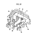
- the transformer 72 to be used in the transformer unit 73 has such a structure that a bobbin 85 has the primary winding 77, the secondary winding 78 and the heater winding 83 wound concentrically and a core 86 is inserted from both sides into the center of the bobbin 85.
- the transformer 72 has a primary connecting pin 87, a secondary connecting pin 88, a heater connecting pin 89 and a ground connecting pin 90 in a bottom portion thereof, and is inserted in the through hole of the printed board 71 to be a mounting source and is connected to the circuit pattern of the printed board 71 by soldering.
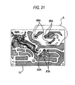
- Fig. 21 shows an example of the circuit pattern of the printed board 71, in which through holes 87A, 88A, 89A and 90A for inserting the primary connecting pin 87, the secondary connecting pin 88, the heater connecting pin 89 and the ground connecting pin 90 in the transformer 72 therethrough are formed.
- the through holes 88A and 89A inserting the secondary connecting pin 88 and the heater connecting pin 89 of the transformer 72 therethrough are formed in a high-voltage component region A, respectively.
- a part of the transformer 72 is mounted, and furthermore, high-voltage components constituting the voltage doubler rectifying circuit 81, for example, the capacitor 79 and the diode 80 are mounted.
- various components constituting a weak voltage circuit such as a control circuit are mounted.
- the transformer having the structure shown in Fig. 19 has been described in JP-A-2001-189221 gazette ( Fig. 3 ), for example.
- the high-frequency heating device has required a reduction in a size and an enhancement in a function. Therefore, there has been used a component having the size of each portion reduced and a higher added value.
- the high-voltage components such as the capacitor 79 and the diode 80 which constitute the voltage doubler rectifying circuit 81 are much larger than components constituting the control circuit, and the size of the high-voltage component region A of the printed board 71 is increased in order to maintain a space for mounting these high-voltage components.
- the transformer unit 73 it is necessary to increase an interval between circuit patterns in order to prevent a leakage between the primary side to be the input side of the transformer 72 and the secondary side having a high voltage to be the output side. Consequently, the size of the high-voltage component region A in the printed board 71 is to be increased.
- the size of the high-voltage component region A is to be increased. Therefore, the printed board 71 itself becomes large-sized so that it is hard to meet the requirement for reducing the size of the high-frequency heating device.
- the high-voltage components such as the capacitor 79 and the diode 80 which constitute the voltage doubler rectifying circuit 81 are mounted on another small board 91, and the small board 91 is also erected on the printed board 71.
- the small board 91 is required separately. Consequently, a cost is increased.
- a large installation space in the printed board 71 is occupied by the small board 91. Thus, the size cannot be reduced.
- JP 2106007 describes a transformer surrounded by an insulating case. In order to have a temperature fuse in the vicinity of the transformer a holding section is attached to the inside of the insulating case.
- the invention has been made in consideration of the circumstances and has an object to provide a transformer and a transformer unit having the transformer which can decrease an occupied space in a printed board to carry out space saving and can reduce the size of the unit without sacrificing the performance of the transformer and increasing a cost. This can be achieved by the features of the independent claim.
- the component holding section for holding a component is provided in the outerperipheral portion excluding the mounting side on the printed board, for example, the side surface of the bobbin.
- the component holding section is formed on the component fixing plate to be the separate member from the bobbin. Therefore, a work for attaching a component is carried out for the single component fixing plate. Thus, the work can be simplified. Moreover, it is easy to automatically assemble the component. Consequently, an assembly cost can be reduced.
- the bobbin is divided into the bobbin base member and the side end flange section, and the component holding section is formed in the side end flange section to be a separate member from the bobbin base member. Consequently, a work for attaching a component is carried out for the single side end flange section. Thus, the work can be simplified.
- the component held by the component holding section is covered with the insulating cover. Consequently, it is possible to prevent the generation of a short circuit, thereby maintaining a high safety.
- the end of the secondary winding is protruded from the outer peripheral portion excluding the mounting side on the printed board.
- the secondary winding can be directly connected to the end. Consequently, it is possible to lessen circuit patterns on the printed board.
- the lead wires of the components held by the component holding section or the lead wire and the end to be the lead wire of the secondary winding are connected directly. Therefore, it is possible to further reduce and simplify a circuit pattern in the printed board.
- a comparatively large high-voltage component constituting the voltage doubler rectifying circuit for rectifying the high voltage having the high frequency from the secondary winding is held by the component holding section of the transformer. Therefore, it is possible to minimize an occupied space by mounting a component on the printed board. Thus, it is possible to reduce a size without sacrificing the performance of the transformer and increasing a cost.
- a suitable transformer unit for example.
- a conductor strand used in the secondary winding is very thin. For this reason, there is a possibility that the secondary winding might be cut if a constant tension or more acts on the connecting end of the secondary winding connected to a connecting pin due to the run-out and looseness of the component holding section by an operating force in assembly when the transformer is to be assembled into the printed board.
- the connecting end of the secondary winding is connected directly or indirectly to the lead wire of the high-voltage component through the post protruded from the bobbin. Even if a displacement is generated on the lead wire of the high-voltage component, therefore, it can be absorbed by the allowance of the secondary winding provided between the post and the lead wire and the secondary winding can be prevented from being cut.
- a conductor strand used in the secondary winding is very thin as described above. Therefore, the strand becomes fragile due to copper corrosion in solder bonding, and furthermore, becomes fragile due to a damage in welding for non-solder bonding such as fusing. For this reason, there is a possibility that the connecting end of the secondary winding connected to a connecting pin might be cut if a constant tension or more acts on the same connecting end due to the run-out and looseness of the component holding section by a vibration caused when or after the transformer is assembled into the printed board.
- the plate-shaped connecting terminal used for the mutual electrical connection of the lead wires of the high-voltage components has a large radiating surface for the lead wires of these components, for example, and has an excellent radiating property. Therefore, heat generated on each high-voltage component can be efficiently radiated into an ambient atmosphere to prevent the temperature of each high-voltage component from being raised, and at the same time, a stress generated in the connecting portion due to the thermal expansion of the component can be suppressed. Consequently, it is possible to enhance the operating stability of each high-voltage component and to prolong the life of the connecting portion.
- the connecting portion on the heater winding side of the diode and the capacitor can also be connected to one of the leads of the heater winding through a single jumper wire.
- the use of a dummy terminal on the printed board is indispensable in order to support the other lead of the heater winding on a distribution path.
- the leads of the heater winding can be stably supported on the distribution path of the printed board by the connection of the diode and the capacitor. Consequently, the use of the dummy terminal can be omitted.
- one ground connecting terminal also serves as the ground connection of the voltage doubler rectifying circuit and the ground connection of the core.
- the number of the ground connecting terminals to be used can be decreased, and at the same time, the working steps of the ground connection can be reduced.
- the productivity of the transformer unit can be enhanced and a cost can be reduced by a decrease in components.
- the ground connecting terminal can connect the high-voltage component and the core to the ground terminal on the printedboardby a comparatively simple structure including the lead connecting section and the core connecting section.
- the partition wall protruded from the bobbin is provided between the core and the high-voltage component, and the mutual rectilinear communication of the core and the high-voltage component is lacking. Consequently, there can be enhanced an insulating effect between the high-voltage component to which a high voltage is applied and the core to be grounded.
- the insulating effect between the high-voltage component and the core can be enhanced.
- a gap between the core and the high-voltage component can be reduced and the size of the transformer unit can further be reduced.
- the partition wall is extended to be higher than the height of protrusion of the high-voltage component from the bobbin. Consequently, an insulating distance can be maintained to be long and the insulating effect of the core and the high-voltage component can be more enhanced.
- the component holding section for holding a component is provided in the outer peripheral portion excluding the mounting side on the printed board.
- the component holding section By causing the component holding section to hold the high-voltage component, therefore, it is possible to eliminate the mounting of the high-voltage component on the printed board. Accordingly, it is possible to reduce the size of the printed board without sacrificing the performance of the transformer and increasing a cost.
- the size of the transformer unit can be reduced. In use for a high-frequency heating device requiring a reduction in a size and an enhancement in a function, consequently, a suitable transformer unit can be implemented.
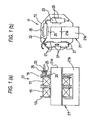
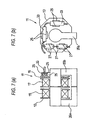
- Fig. 1 is sectional and side views showing the transformer according to the invention
- Fig. 2 is a perspective view showing the transformer
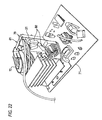
- Fig. 3 is a perspective view showing the transformer unit.
- a transformer 11 to be mounted on the transformer unit according to the invention is mainly constituted by a bobbin 13 formed of a resin, a primary winding 15, a secondary winding 17 and a heater winding 19 which are wound around the bobbin 13, and a core 21.
- the core 21 is constituted by an I-shaped core 21a having a rectangular section which is inserted through the center of the bobbin 13, and a U-shaped core 21b having a U shape seen from a side which is connected to both ends of the I-shaped core 21a, and the transformer 11 is mounted on a printed board 23 with the U-shaped core 21b turned downward.
- the bobbin 13 has a side surface provided with a plurality of (four in total according to the embodiment) component holding sections having pairs of interposing pieces 25 and 27, respectively.
- a capacitor 31 to be a high-voltage component constituting a voltage doubler rectifying circuit 81 is interposed between the pair of interposing pieces 27 and a diode 33 is interposed between the pair of interposing pieces 25.
- the component holding section according to the embodiment is formed with the pairs of interposing pieces 25 and 27 erected on the side surface of the bobbin 13 apart from each other by almost the thickness of the high-voltage component,
- the lead wires of the capacitor 31 and the diode 33 to be the high-voltage components are protruded from the outer peripheral portion excluding the mounting side on the printed board 23, and the connecting ends of the secondary winding 17 and the heater winding 19 are connected to the lead wires based on circuits, respectively. Accordingly, a connecting cord from a magnetron is directly connected without using the printed board 23 in the outer peripheral portion excluding the mounting side of the transformer 11 on the printed board 23.
- the side surface of the bobbin 13 is provided with the component holding sections for holding the high-voltage components such as the condenser 31 and the diode 33.
- the size of the transformer unit 100 can be reduced.
- the suitable transformer unit 100 can be obtained.
- the connecting ends of the secondary winding 17 and the heater winding 19 are connected to the outer peripheral portion excluding the mounting side of the transformer 11 on the printed board 23. Therefore, the connecting cord from the magnetron canbe directly connected to the transformer 11 without using the printed board 23. Consequently, it is possible to lessen circuit patterns in the printed board 23, particularly, it is possible to eliminate the high-voltage circuit pattern of the transformer 11 in which an interval between the patterns is to be increased because of a high voltage. As shown in Fig. 3 , therefore, the size of the printed board 23 can be reduced considerably.
- the circuit pattern in the printed board 23 can further be reduced and simplified.
- a direction in which the transformer 11 is mounted on the printed board 23 is not restricted to a direction in which the U-shaped core 21b of the core 21 shown in Fig. 3 described above is set onto an underside but it is also possible to employ a configuration in which the I-shaped core 21a is provided perpendicularly to the printed board 23 as shown in Fig. 4 , a configuration in which the I-shaped core 21a is provided in parallel with the printed board 23 and the U-shaped core 21b is provided on the side of the transformer 11 as shown in Fig. 5 or a configuration in which the high-voltage components are provided on the printed board 23 side in a lower part as shown in Fig. 6 .
- a clearance corresponding to the protrusion of the I-shaped core 21a from the bobbin 13 is generated between the side surface of the bobbin 13 provided on the lower side of the transformer 11 and the printed board 23, and a component 41 having a flat shape can be mounted on the clearance. Consequently, the mounting surface of the printed board 23 can effectively be utilized so that a space efficiency can be enhanced. Moreover, the height of the transformer 11 from the printed board 23 surface can be reduced so that a mounting stability can be enhanced. Furthermore, a high-voltage component generating heat is provided on an upper surface. Consequently, a heat transfer to the other portions of the transformer 11 can be suppressed during heat radiation so that the influence of the high-voltage component on the transformer 11 can be eliminated.
- a primary winding 15, a secondary winding 17 and a heater winding which have flat shapes are provided vertically in the same manner as those in the structure shown in Fig. 3 . Consequently, the installation area of the printed board 23 can be reduced so that the mounting density of the printed board 23 can be enhanced.
- a distance between each winding and a printed board is increased so that the superposition of a noise on the circuit of the printed board can be prevented as much as possible.
- terminal of the heater winding and the lead wire terminal to be connected to the magnetron are provided on the transformer 11 side in the transformer units 100 to 400, it is also possible to employ such a structure that these terminal sections are connected to the printed board 23. More specifically, these terminal sections are connected to the circuit pattern of the printed board 23 and are connected from the printed board 23 to the magnetron by a high-voltage lead wire through a tab terminal. By changing a length on the high-voltage lead wire side which carries out a connection from the printed board 23 to the magnetron, thus, it is not necessary to change a wiring length to the magnetron for each type of the unit.
- a transformer 11 shown in Fig. 7 uses two U-shaped cores 35a and 35b formed to have identical shapes to each other in place of the core 21 including the I-shaped core 21a and the U-shaped core 21b, and the U-shaped cores 35a and 35b are inserted from both end sides of a bobbin 13.
- the portions of the U-shaped cores 35a and 35b to be inserted into the bobbin 13 are formed to have circular sections.
- the cores 35a and 35b are formed to have the identical shapes to each other. Consequently, the productivity of each of the cores 35a and 35b can be enhanced and a work for assembling them can also be simplified because it is not necessary to distinguish both of them.
- the wound portion of a winding on the center of the bobbin 13 can also have a circular section. Consequently, it is possible to smoothly carry out a work for winding a primary winding 15, a secondary winding 17 and a heater winding 19 without the influence of a change in a circumferential speed in case of a square section.
- the high-voltage components of a component fixing plate 43 constituted separately from the bobbin 13 having the primary winding 15, the secondary winding 17 and the heater winding 19 wound therearound are attached to the bobbin 13.
- Interposing pieces 25 and 27 according to an example of a component holding section are formed on the component fixing plate 43, and a capacitor 31 and a diode 33 which are the high-voltage components are fixed thereto.
- the high-voltage components are assembled into the component fixing plate 43 before each winding process and the component fixing plate 43 is connected to the bobbin 13 through bonding means which is not shown.
- the winding process can be carried out in a state in which the component fixing plate 43 and the bobbin 13 are integrated with each other. Consequently, it is possible to easily carry out a processing for the end of each winding by connecting the end of the winding to the lead wire of the high-voltage component after the winding process. Thus, a workability can be enhanced, and furthermore, the handling property of the transformer itself can be improved.
- the insulating cover 45 is attached to the side of the bobbin 13 so that the high-voltage components 31 and 33 are accommodated in the insulating cover 45 and can be prevented from being exposed to the outside. Consequently, the generation of a short circuit can be prevented so that a high safety can be maintained.
- the insulating cover 45 may have a structure in which a component holding section for fixing the high-voltage components is further formed on an internal surface to fix the high-voltage components on the insulating cover 45 side. It is preferable that a radiation hole for radiating the heat of the high-voltage components should be properly provided on the insulating cover 45.
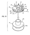
- a bobbin comprises a bobbin base member 47 for wining at least a primary winding and a second winding therearound and a side end flange section 49 attached to one of the ends of the bobbin base member 47, and a component holding section is formed in the side end flange section 49.
- the bobbin base member 47 has a core section 47a and a flange section 47b in such a manner that the primary winding and the secondary winding can be wound therearound, and the side end flange section 49 has a space for winding a heater winding which is formed by an inside flange 49a and an outside flange 49b and interposing pieces 25 and 27 according to an example of the component holding section for fixing high-voltage components are formed on the outside surface of the outside flange 49b.
- the bobbin base member 47 and the side end flange section 49 are connected to each other through bonding means which is not shown, and are thus integrated.
- the high-voltage component is assembled into the side end flange section 49 and the heater winding is attached before the process of each winding of the bobbin base member 47, the side end flange section 49 is connected to the bobbin base member 47 and the winding processes for the primary winding and the secondary winding can be carried out in a state in which the bobbin base member 47 and the side end flange section 49 are integrated. Consequently, it is possible to easily carry out the process for the end of each winding by connecting the end of the winding to the lead wire of the high-voltage component after the winding process. Thus, a workability can be enhanced, and furthermore, the handling property of the transformer itself can be improved.
- the component holding section is formed on a separate member from the bobbin base member 47. Therefore, a work for attaching components can be prevented from being complicated. Thus, the work can be simplified. Moreover, the components can easily be assembled automatically so that an assembly cost can be reduced.
- Figs. 11 to 14 show a further embodiment of the transformer unit according to the invention.
- a pair of U-shaped cores 35a and 35b are inserted fromboth end sides of abobbin 13, and a core is attached to a printed board 23 around the outside of the bobbin 13 in such a configuration as to be set in the side position of the bobbin 13 provided apart from the printed board 23 by a constant distance.
- the central axis of the bobbin 13 is parallel with the printed board 23. Therefore, a primary winding 15, a secondary winding 17 and a heater winding 19 are provided vertically with respect to the printed board 23.
- interposing pieces 26 and 28 to be component holding sections for interposing the lead wires of high-voltage components constituting a voltage doubler rectifying circuit 93 for rectifying a high voltage having a high frequency from the secondary winding 17 are protruded from the secondary winding 17 and the heater winding 19 in the bobbin 13.
- each of the interposing pieces 26 and 28 is provided with an engagement groove for tightly fitting the lead wire, and the interposing piece 26 serves to hold a diode 33 and the interposing piece 28 serves to hold a capacitor 31.
- a circuit for the transformer unit 500 according to the embodiment has a structure shown in Fig. 13 .
- a commercial power source 74 is full-wave rectified by a rectifying circuit 75 such as a diode bridge and is converted into a high-frequency voltage by an inverter 76, and the high-frequency voltage is applied to the primary winding 15 of the transformer 11. Consequently, a high voltage having a high frequency of several kV is generated on the secondary winding 17 of the transformer 11.
- the high voltage having the high frequency is rectified by the voltage doubler rectifying circuit 93 comprising the capacitor 31 and the diode 33.
- the high voltage is applied to a magnetron 82 to be a microwave generator.
- the heater winding 19 of the transformer 11 is connected to a filament 84 of the magnetron 82 to heat the filament 84.
- the magnetron 82 oscillates a microwave by heating the filament 84 and applying the high voltage.
- the capacitor 31 and the diode 33 to be the high-voltage components provided on the component holding sections have a relay terminal 51 bonded to a leadwire L connected to the secondary winding 17 and the heater winding 19 through spot welding.
- the relay terminal 51 is formed by a metal plate such as a phosphor bronze plate, for example, and includes a hook-shaped tip portion 51a winding and connecting a winding M, a base end 51b bonded to the lead wire L of the high-voltage component, and a flexible portion 51c opposed to the tip portion 51a as shown in Fig. 14(a) .
- Both the connecting end of the secondary winding 17 and that of the heater winding 19 are connected to the relay terminal 51 through a post 22 protruded from the bobbin 13.
- the relay terminal 51 is utilized to carry out the soldering.
- the soldering cannot be carried out, moreover, it is possible to perform fusing by giving a large current while causing the mutual opposed portions 51a and 51c of the relay terminal 51 to be close to each other by pressure as shown in Fig. 14(b) .
- the windings 17 and 19 are once held by the post 22.
- the post 22 receives a stress against the fragility caused by a stress in welding such as fusing so that a stress in the relay terminal 51 portion can be minimized.
- Winding connecting portions 1) to 4) obtained by the relay terminal 51 shown in Fig. 12 correspond to connecting portions 1) to 4) on a circuit diagram of Fig. 13 .
- the connecting portion 1) is provided between one of the connecting ends of the secondary winding 17 and a pair of capacitors 31, and the connecting portion 2) is provided between the other connecting end of the secondary winding 17 and a pair of diodes 33.
- the connecting portion 3) is provided between one of the leads of the heater winding 19 and a lead L of the anode of the diode 33, and the connecting portion 4) is provided between the other lead of the heater winding 19 and the lead L of the capacitor 31.
- conductor strands used in the secondary winding 17 and the heater winding 19 are very thin. For this reason, there is a possibility that the conductor strands might be cut if a constant tension or more acts on the connecting ends of the secondary winding 17 and the heater winding 19 due to the run-out and looseness of the component holding section by an operating force in assembly and a vibration generated during transportation when the transformer 11 is to be assembled into the printed board 23.
- the mutual electrical connection of the lead wires of the high-voltage components provided on the component holding section is not carried out directly but through a plate-shaped connecting terminal 53 as shown in Figs. 11 and 12 .
- the plate-shaped connecting terminal 53 is used in a portion in which a pair of diodes 33 and 33 are mutually connected in series.
- a metal plate having an excellent characteristic in a radiating property (a thermal conductivity) as well as an electrical conductivity is preferable, and a phosphor bronze plate can be used, for example.
- the connecting terminal 53 has a large radiating surface for the lead wires of the high-voltage components and has an excellent radiating property. Therefore, heat generated on each high-voltage component can be efficiently radiated into an ambient atmosphere to prevent the temperature of each high-voltage component from being raised, and at the same time, a stress generated in the connecting portion due to the thermal expansion of the component can be suppressed. Consequently, it is possible to enhance the operating stability of each high-voltage component and to prolong the life of the connecting portion.
- the diode 33 and the capacitor 31 in the voltage doubler rectifying circuit 93 to be connected to the heater winding 19 incorporated in the transformer 11 are individually connected to the heater winding 19, that is, the lead terminal of the diodes 33 connected in series is connected to one of the leads of the heater winding 19 and the lead terminal of the capacitors 31 connected in series is connected to the other lead of the heater winding 19 as shown in 3) and 4) of Fig. 13 .
- the relay terminal 51 is used for the connection of the respective lead terminals and the windings as described above.
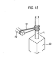
- the secondary winding 17 and the heater winding 19 are bonded to the lead wire L of the high-voltage component through the relay terminal 51 in the embodiment, it is also possible to employ a structure in which the relay terminal is omitted and the secondary winding 17 and the heater winding 19 are soldered to the lead wire L of the high-voltage component via the post 22 protruded from the bobbin 13 and are thus bonded directly as shown in Fig. 15 .
- the displacement of the lead wire L of the high-voltage component can be absorbed in the allowances of the windings 17 and 19 provided between the post 22 and the lead wire L.
- the windings 17 and 19 can be prevented from being cut.
- the windings 17 and 19 are once held by the post 22. Consequently, it is possible to eliminate the fragility of the windings 17 and 19 which is caused by high-temperature soldering corresponding to unleading.
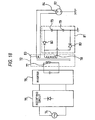
- the connecting portion of the diode 33 and the capacitor 31 is connected to one of the leads of the heater winding through a single jumper wire as shown in a circuit diagram of Fig. 18 .
- the use of a dummy terminal on the bobbin 13 is indispensable in order to support the other lead of the heater winding on a distribution path.
- the leads of the heater winding 19 can be stably supported on the distribution path by the connection of the diode 33 and the capacitor 31. Consequently, the use of the dummy terminal on the bobbin 13 can be omitted.
- the reason why the dummy terminal can be omitted is that a voltage obtained by the voltage doubler rectifying circuit 93 is 100 to 500 times as high as a voltage generated on both ends of the heater winding 19, resulting in apparently the same motion as that of the circuit shown in Fig. 18 .
- a ground connecting terminal 55 for connecting the voltage doubler rectifying circuit 93 provided on the component holding section to a ground contact 24 provided on the printed board 23 is obtained by forming a metal wire having an excellent electrical conductivity and spring property to take a predetermined shape and includes a lead connecting section 55a connected to the lead wire L of the high-voltage component constituting the voltage doubler rectifying circuit 93 (the cathode of the diode 33 in the example), and a board connecting section 55b connected to the ground contact 24 provided on the printed board 23.
- a core connecting section 55c for implementing a conduction with the core 35b of the transformer 11 in elastic contact with the external surface of the core 35b is integrally formed between the lead connecting section 55a and the board connecting section 55b.
- ground connecting terminal 55 In the case in which the ground connecting terminal 55 is used for a ground connection, one ground connecting terminal 55 serves to carry out the ground connection of the voltage doubler rectifying circuit 93 and that of the core 35b. As compared with the case in which the ground connections are to be individually carried out, therefore, the number of uses of the ground connecting terminal 55 can be decreased, and at the same time, the working steps of the ground connection can be reduced. Consequently, the productivity of the transformer unit can be enhanced and a cost can be reduced by a decrease in components.
- the ground connecting terminal 55 is attached after a breakdown voltage test for the transformer 11. Therefore, it is possible to execute the breakdown voltage test for the transformer 11 while mounting the diode 33.
- Fig. 16 shows an embodiment in which a partition wall is provided on the bobbin of the transformer unit according to the invention.
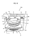
- a pair of U-shaped cores 35a and 35b are inserted fromboth end sides of abobbin 13, and a core is attached to a printed board 23 around the outside of the bobbin 13 in such a configuration as to be set in the side position of the bobbin 13 provided apart from the printed board 23 by a constant distance.
- the central axis of the bobbin 13 is parallel with the printed board 23. Therefore, a primary winding 15, a secondary winding 17 and a heater winding 19 are provided vertically with respect to the printed board 23.
- Interposing pieces 26 and 28 to be component holding sections for interposing the lead wires of high-voltage components constituting a voltage doubler rectifying circuit 93 (see Fig. 13 ) for rectifying a high voltage having a high frequency from the secondary winding 17 are protruded from the secondary winding 17 and the heater winding 19 in the bobbin 13 ( Fig. 16 shows only the interposing piece 26. See Fig. 12 for the interposing piece 28.).
- each of the interposing pieces 26 and 28 is provided with an engagement groove for tightly fitting the lead wire, and the interposing piece 26 serves to hold a diode 33 and the interposing piece 28 serves to hold a capacitor 31.
- the capacitor 31 and the diode 33 have a relay terminal 51 bonded to a lead wire connected to the secondary winding 17 and the heater winding 19 through spot welding. Both the connecting end of the secondary winding 17 and that of the heater winding 19 are connected to the relay terminal 51 via a post 22 protruded from the bobbin 13. Moreover, the mutual electrical connection of the lead wires of the high-voltage components provided on the component holding section is not carried out directly but through a plate-shaped connecting terminal 53.
- a partition wall 61 for separating the core 35b from the capacitor 31 and the diode 33 to be the high voltage components held by the interposing pieces 26 and 28 is erected in the outer peripheral portion of the bobbin 13 in which the interposing pieces 26 and 28 to be the component holding sections are formed.
- the partition wall 61 is extended to be higher than the height of protrusion of the high-voltage component from a bobbin side surface 13a holding at least the same component and is provided to be present on a straight line connecting the high-voltage component to the core 35b.
- the partition wall 61 is formed integrally with the bobbin 13, a separate member may be fixed to the bobbin 13.
- the partition wall 61 should be formed cylindrically to surround the core 35b, moreover, it is possible to divide a portion in which a very great advantage cannot be produced on the insulating effect from the high-voltage components (for example, a position corresponding to the non-electrode portion of the high-voltage component) as shown in the drawing and to form the same portion to take a U shape as in the example.
- a stopper (not shown) for preventing the core 35b from slipping from the bobbin 13 is engaged in the dividing position of the partition wall 61 according to the embodiment.
- the partition wall 61 protruded from the bobbin 13 is provided between the core 35b and the high-voltage component. Accordingly, the mutual rectilinear communication of the core 35b and the high-voltage component is lacking. Consequently, it is possible to enhance the insulating effect between the high-voltage component to which a high voltage is applied and the core 35b to be grounded. Thus, it is possible to reliably prevent an insulation from being deteriorated by a discharge between the core 35b and the high-voltage component or dust collected for a long period of time between the core 35b and the high-voltage component. Moreover, the insulating effect between the high-voltage component and the core 35b can be enhanced. As compared with a structure in which the partition wall 61 is not provided, therefore, a gap between the core 35b and the high-voltage component can be reduced and the size of the transformer unit 600 can further be decreased.
- a place in which the high-voltage component is to be held is not restricted to the side surface of the bobbin 13 but may be in any other position in the outer peripheral portion of the transformer 11 excluding the mounting side on the printed board 23.
- the component holding section can also be formed on the component fixing plate constituted separately from the bobbin 13 so as to be integrated with the bobbin 13.
- the component holding section for holding a component is provided in the outer peripheral portion excluding the mounting side on the printed board.
- the component holding section By causing the component holding section to hold the high-voltage component, therefore, it is possible to eliminate the mounting of the high-voltage component on the printed board. Accordingly, it is possible to reduce the size of the printed board without sacrificing the performance of the transformer and increasing a cost.
- the size of the transformer unit can be reduced. In use for a high-frequency heating device requiring a reduction in a size and an enhancement in a function, consequently, a suitable transformer unit can be implemented.
Landscapes
- Engineering & Computer Science (AREA)
- Power Engineering (AREA)
- Physics & Mathematics (AREA)
- Electromagnetism (AREA)
- Manufacturing & Machinery (AREA)
- Control Of High-Frequency Heating Circuits (AREA)
- Coils Of Transformers For General Uses (AREA)
Claims (16)
- Transformator (11), der umfasst:einen Spulenkörper (13), auf den wenigstens eine Primärwicklung (15) und eine Sekundärwicklung (17) gewickelt sind,einen Kern (21), der durch eine Mitte des Spulenkörpers eingeführt und auf einer Leiterplatte (23) montiert ist,dadurch gekennzeichnet, dass ein Bauteil-Halteabschnitt zum Halten eines Bauteils in einem Außenumfangsabschnitt des Spulenkörpers (13) mit Ausnahme einer Montageseite an der Leiterplatte vorhanden ist, wobei der Bauteil-Halteabschnitt Einfügestücke (25, 27) umfasst.
- Transformator nach Anspruch 1, wobei der Bauteil-Halteabschnitt an einer Seitenfläche des Spulenkörpers (13) ausgebildet ist.
- Transformator nach Anspruch 1, wobei der Bauteil-Halteabschnitt auf einer Bauteil-Befestigungsplatte (43) als ein von dem Spulenkörper (13) separates Element ausgebildet ist, und die Bauteil-Befestigungsplatte (43) an dem Spulenkörper (13) befestigt ist.
- Transformator nach Anspruch 1, wobei der Spulenkörper ein Spulenkörper-Trägerelement (47) zum Aufwickeln wenigstens der Primärwicklung und der Sekundärwicklung darauf und einen seitlichen Abschlussflanschabschnitt (49) umfasst, der an einem der Enden des Spulenkörper-Trägerabschnitts (47) anzubringen ist, und der Bauteil-Halteabschnitt in dem seitlichen Abschlussflanschabschnitt (49) ausgebildet ist.
- Transformator nach einem der Ansprüche 1 bis 4, der des Weiteren eine isolierende Abdeckung (45) zum Abdecken eines durch den Bauteil-Halteabschnitt gehaltenen Bauteils, die an der Seite des Spulenkörpers (13) angebracht ist, umfasst.
- Transformator nach einem der Ansprüche 1 bis 5, wobei ein Ende der Sekundärwicklung (17) von dem Außenumfangsabschnitt mit Ausnahme der Montageseite an der Leiterplatte (23) vorsteht.
- Transformator nach Anspruch 6, wobei wenigstens einer der Zuleitungsdrähte eines Bauteils, das von einem Bauteil-Halteabschnitt gehalten wird, und die Verbindungsenden der Sekundärwicklung mit einem Zuleitungsdraht eines Bauteils verbunden sind, das von einem anderen Bauteil-Halteabschnitt gehalten wird.
- Transformatoreinheit (100), die den Transformator nach einem der Ansprüche 1 bis 7 an einer Leiterplatte anbringt, wobei sie umfasst:eine Spannungsverdoppler-Gleichrichterschaltung (93) zum Gleichrichten einer Hochspannung mit einer hohen Frequenz von der Sekundärwicklung (17) des Transformators (11), wobei ein Hochspannungsbauteil, das die Spannungsverdoppler-Gleichrichterschaltung (93) bildet, in dem Bauteil-Halteabschnitt gehalten wird.
- Transformatoreinheit (100) nach Anspruch 8, wobei
ein Verbindungsende der Sekundärwicklung (17) über einen Ausleger (22), der von dem Spulenkörper (13) vorsteht, direkt oder indirekt mit einem Zuleitungsdraht eines Hochspannungsbauteils verbunden ist. - Transformatoreinheit nach Anspruch 9, wobei ein plattenförmiger Übertragungsanschluss (51) mit dem Zuleitungsdraht des Hochspannungsbauteils (L) verbunden ist, der Verbindung mit dem Verbindungsende der Sekundärwicklung (17) herstellt, und das Verbindungsende der Sekundärwicklung (17) mit dem Übertragungsanschluss (51) verbunden ist.
- Transformatoreinheit (100) nach einem der Ansprüche 8 bis 10, wobei eine gegenseitige elektrische Verbindung der Zuleitungsdrähte der Hochspannungsbauteile, die an dem Bauteil-Halteabschnitt vorhanden sind, über einen plattenförmigen Verbindungsanschluss (53) ausgeführt ist, der als eine Strahlungsplatte dient.
- Transformatoreinheit (100) nach einem der Ansprüche 8 bis 11, wobei bei einem Paar Dioden (33), die in Reihe verbunden sind, und einem Paar Kondensatoren (31), die in der Spannungsverdoppler-Gleichrichterschaltung in Reihe verbunden sind, ein Zuleitungsanschluss der Diode (33) mit einem der Leiter einer Heizwicklung (19) verbunden ist, die in den Transformator (11) integriert ist, und ein Zuleitungsanschluss des Kondensators (31) mit der anderen Zuleitung der Heizwicklung (19) verbunden ist.
- Transformatoreinheit (100) nach einem der Ansprüche 8 bis 12,
wobei die Spannungsverdoppler-Gleichrichterschaltung (93) und der Kern mit einem Erdanschluss an der Leiterplatte (23) über einen gemeinsamen Erdverbindungsanschluss (55) verbunden sind. - Transformatoreinheit (100) nach Anspruch 13, wobei der Erdverbindungsanschluss (55) einen Zuleitungs-Verbindungsabschnitt (55a), der mit einem Zuleitungsdraht (L) eines Hochspannungsbauteils zu verbinden ist, das die Spannungsverdoppler-Gleichrichterschaltung (93) bildet, und einen Platten-Verbindungsabschnitt (55b) enthält, der mit einem Erdkontakt (24) zu verbinden ist, und einen Kern-Verbindungsabschnitt (55c), der eine Leitung zu einem Kern (35b) herstellt, in elastischem Kontakt mit einer Außenfläche des Kerns zwischen dem Leiter-Verbindungsabschnitt (55a) und dem Platten-Verbindungsabschnitt (55b) vorhanden ist.
- Transformatoreinheit (100) nach einem der Ansprüche 8 bis 14, wobei eine Trennwand (61) zum Trennen des Kerns (35b) von dem Hochspannungsbauteil, das von dem Bauteil-Halteabschnitt gehalten wird, in einem Außenumfangsbereich des Spulenkörpers (13) aufgerichtet ist, der mit dem Bauteil-Halteabschnitt versehen ist.
- Transformatoreinheit (100) nach Anspruch 15, wobei die Trennwand (61) sich so erstreckt, dass sie höher ist als eine Höhe, um die das Hochspannungsbauteil von dem Spulenkörper (13) vorsteht.
Applications Claiming Priority (7)
| Application Number | Priority Date | Filing Date | Title |
|---|---|---|---|
| JP2002269961 | 2002-09-17 | ||
| JP2002269961 | 2002-09-17 | ||
| JP2003076138 | 2003-03-19 | ||
| JP2003076138 | 2003-03-19 | ||
| JP2003270939 | 2003-07-04 | ||
| JP2003270939A JP4184179B2 (ja) | 2002-09-17 | 2003-07-04 | トランス及びそれを備えたトランスユニット |
| PCT/JP2003/011853 WO2004027792A1 (en) | 2002-09-17 | 2003-09-17 | Transformer and transformer unit having the same |
Publications (2)
| Publication Number | Publication Date |
|---|---|
| EP1540674A1 EP1540674A1 (de) | 2005-06-15 |
| EP1540674B1 true EP1540674B1 (de) | 2008-04-02 |
Family
ID=32034066
Family Applications (1)
| Application Number | Title | Priority Date | Filing Date |
|---|---|---|---|
| EP03755678A Expired - Lifetime EP1540674B1 (de) | 2002-09-17 | 2003-09-17 | Transformator und transformatoranordnung mit solchem transformator |
Country Status (7)
| Country | Link |
|---|---|
| US (1) | US6970065B2 (de) |
| EP (1) | EP1540674B1 (de) |
| JP (1) | JP4184179B2 (de) |
| CN (2) | CN100338699C (de) |
| AU (1) | AU2003273520A1 (de) |
| DE (1) | DE60320114T2 (de) |
| WO (1) | WO2004027792A1 (de) |
Families Citing this family (17)
| Publication number | Priority date | Publication date | Assignee | Title |
|---|---|---|---|---|
| JP4184179B2 (ja) * | 2002-09-17 | 2008-11-19 | 松下電器産業株式会社 | トランス及びそれを備えたトランスユニット |
| JP3901669B2 (ja) * | 2003-07-04 | 2007-04-04 | 松下電器産業株式会社 | トランスユニット載置プリント基板 |
| JP4006369B2 (ja) * | 2003-07-08 | 2007-11-14 | 松下電器産業株式会社 | トランス装置及びその製造方法 |
| JP2006129687A (ja) * | 2004-10-01 | 2006-05-18 | Nec Tokin Corp | Acアダプタ |
| AT501054B8 (de) * | 2004-10-25 | 2007-02-15 | Moeller Gebaeudeautomation Kg | Differenzstromwandler |
| US7854616B2 (en) * | 2007-10-12 | 2010-12-21 | The L.D. Kichler Co. | Positionable lighting systems and methods |
| US8102237B2 (en) | 2008-06-12 | 2012-01-24 | Power Integrations, Inc. | Low profile coil-wound bobbin |
| US20100271159A1 (en) * | 2009-03-10 | 2010-10-28 | Nikon Corporation | Electromagnetic Coil Design for Improved Thermal Performance |
| JP2011142196A (ja) * | 2010-01-07 | 2011-07-21 | Panasonic Corp | トランスユニット |
| CN103383889B (zh) * | 2013-06-27 | 2016-02-03 | 广安市华蓥山领创电子有限公司 | 一种超薄变压器骨架 |
| TWM476419U (en) * | 2014-01-09 | 2014-04-11 | Delta Electronics Inc | Inverter and bobbin thereof |
| JP2019110145A (ja) * | 2016-03-24 | 2019-07-04 | 株式会社日立製作所 | 変圧器 |
| JP6512451B2 (ja) * | 2016-03-29 | 2019-05-15 | 株式会社オートネットワーク技術研究所 | 電源装置 |
| CN108806958B (zh) * | 2018-08-14 | 2024-07-05 | 江苏保丽洁环境科技股份有限公司 | 干式高压变压器 |
| CN109065336B (zh) * | 2018-09-20 | 2024-07-19 | 广东尚研电子科技股份有限公司 | 一种微波变频电源的变压装置及其制造方法 |
| CN112821786B (zh) * | 2021-02-04 | 2022-09-30 | 兰州大学 | 一种紧凑型负高压直流电源 |
| CN113643885B (zh) * | 2021-08-16 | 2024-05-14 | 上海激光电源设备有限责任公司 | 初级线圈结构及其高压脉冲变压器 |
Family Cites Families (13)
| Publication number | Priority date | Publication date | Assignee | Title |
|---|---|---|---|---|
| US3931549A (en) * | 1974-10-24 | 1976-01-06 | General Signal Corporation | Control circuit for electromagnetic transducer |
| US4503413A (en) * | 1982-12-09 | 1985-03-05 | Telefonbau Und Normalzeit Gmbh | Spool for transformer in power supply device |
| KR910001986B1 (ko) | 1987-04-30 | 1991-03-30 | 마쯔시다덴기산교 가부시기가이샤 | 마그네트론 급전장치 |
| US4939623A (en) * | 1989-04-25 | 1990-07-03 | Universal Data Systems, Inc. | Modem with improved transformer assembly |
| JP2734923B2 (ja) | 1993-03-10 | 1998-04-02 | 松下電器産業株式会社 | 高圧トランス |
| JP3387155B2 (ja) * | 1993-06-30 | 2003-03-17 | 松下電器産業株式会社 | 高圧発生用トランス装置 |
| US5625520A (en) | 1993-11-19 | 1997-04-29 | Daewoo Electronics Co., Ltd. | Device for preventing a high voltage transformer of a microwave oven from being overheated |
| JP3412317B2 (ja) * | 1995-02-27 | 2003-06-03 | 株式会社村田製作所 | フライバックトランス |
| JPH09162052A (ja) * | 1995-12-13 | 1997-06-20 | Murata Mfg Co Ltd | フライバックトランスおよびその組立方法 |
| JP2001189221A (ja) | 1999-12-28 | 2001-07-10 | Tabuchi Electric Co Ltd | ギャップ付コアを備えたトランス |
| JP2001244111A (ja) * | 2000-02-29 | 2001-09-07 | Sanden Corp | コイルボビン |
| US6483412B1 (en) * | 2001-05-03 | 2002-11-19 | Conev Inc. | Transformer or inductor containing a magnetic core |
| JP4184179B2 (ja) * | 2002-09-17 | 2008-11-19 | 松下電器産業株式会社 | トランス及びそれを備えたトランスユニット |
-
2003
- 2003-07-04 JP JP2003270939A patent/JP4184179B2/ja not_active Expired - Lifetime
- 2003-09-16 US US10/663,634 patent/US6970065B2/en not_active Expired - Lifetime
- 2003-09-17 DE DE60320114T patent/DE60320114T2/de not_active Expired - Lifetime
- 2003-09-17 CN CNB031255833A patent/CN100338699C/zh not_active Expired - Lifetime
- 2003-09-17 CN CNU032375476U patent/CN2659083Y/zh not_active Expired - Lifetime
- 2003-09-17 AU AU2003273520A patent/AU2003273520A1/en not_active Abandoned
- 2003-09-17 WO PCT/JP2003/011853 patent/WO2004027792A1/en not_active Ceased
- 2003-09-17 EP EP03755678A patent/EP1540674B1/de not_active Expired - Lifetime
Also Published As
| Publication number | Publication date |
|---|---|
| US6970065B2 (en) | 2005-11-29 |
| JP4184179B2 (ja) | 2008-11-19 |
| US20040113740A1 (en) | 2004-06-17 |
| DE60320114D1 (de) | 2008-05-15 |
| DE60320114T2 (de) | 2009-06-18 |
| CN1496214A (zh) | 2004-05-12 |
| EP1540674A1 (de) | 2005-06-15 |
| JP2004304142A (ja) | 2004-10-28 |
| CN2659083Y (zh) | 2004-11-24 |
| WO2004027792A1 (en) | 2004-04-01 |
| CN100338699C (zh) | 2007-09-19 |
| AU2003273520A1 (en) | 2004-04-08 |
Similar Documents
| Publication | Publication Date | Title |
|---|---|---|
| US6970065B2 (en) | Transformer and transformer unit having the same | |
| JP6893936B2 (ja) | 電解コンデンサ | |
| EP1183920B1 (de) | LEITERPLATTE MIT EINER ISOLIERBARRIERE, Herstellungsverfahren einer solchen Barriere und einer solchen Platte | |
| JP4300717B2 (ja) | Dc−dcコンバータ及びその製造方法 | |
| JP2009212141A (ja) | 電源トランス及びインダクタンス部品 | |
| KR20010029670A (ko) | 부품실장기판 및 부품실장기판의 제조방법 | |
| JP4531736B2 (ja) | トランスユニット | |
| US20120281445A1 (en) | Transformer unit | |
| KR101065454B1 (ko) | 트랜스 장치 및 그 제조 방법과 이를 갖는 고주파 가열장치 | |
| JP3329597B2 (ja) | インダクタンス装置 | |
| JPH07161462A (ja) | 高周波加熱装置 | |
| JP5451860B1 (ja) | スイッチング電源装置 | |
| CN101932151B (zh) | 微波炉的变压器搭载基板装置 | |
| JP4793758B2 (ja) | インダクタンス素子 | |
| JP3901669B2 (ja) | トランスユニット載置プリント基板 | |
| JP2893677B1 (ja) | 電源装置およびその製造方法 | |
| KR102898336B1 (ko) | 노이즈 개선을 위한 전자 제품 패키지 | |
| JP4229947B2 (ja) | 制御装置一体型回転電機およびその製造方法 | |
| JP2004063223A (ja) | 無電極放電ランプ | |
| JPH11214228A (ja) | 電源装置の主トランスおよびその製造方法 | |
| JP3126624B2 (ja) | 電源装置用トランス | |
| JP2004103351A (ja) | マグネトロン駆動電源 | |
| JP3102146B2 (ja) | フライバックトランス | |
| KR200317036Y1 (ko) | 교류발전기 회로판의 콘덴서 조립구조 | |
| JP2002151641A (ja) | 電子部品のモジュール装置 |
Legal Events
| Date | Code | Title | Description |
|---|---|---|---|
| PUAI | Public reference made under article 153(3) epc to a published international application that has entered the european phase |
Free format text: ORIGINAL CODE: 0009012 |
|
| 17P | Request for examination filed |
Effective date: 20050308 |
|
| AK | Designated contracting states |
Kind code of ref document: A1 Designated state(s): AT BE BG CH CY CZ DE DK EE ES FI FR GB GR HU IE IT LI LU MC NL PT RO SE SI SK TR |
|
| AX | Request for extension of the european patent |
Extension state: AL LT LV MK |
|
| DAX | Request for extension of the european patent (deleted) | ||
| RBV | Designated contracting states (corrected) |
Designated state(s): DE FR GB |
|
| 17Q | First examination report despatched |
Effective date: 20060825 |
|
| RIN1 | Information on inventor provided before grant (corrected) |
Inventor name: MORIKAWA, HISASHI Inventor name: SAKAI, SHINICHI Inventor name: SHIROKAWA, NOBUO Inventor name: SATOU, KEIICHI Inventor name: SUENAGA, HARUO Inventor name: YASUI, KENJI,C/O MATSUSHITA ELECTRIC IND. CO, LTD Inventor name: ODA, YOSHITAKA |
|
| GRAP | Despatch of communication of intention to grant a patent |
Free format text: ORIGINAL CODE: EPIDOSNIGR1 |
|
| GRAS | Grant fee paid |
Free format text: ORIGINAL CODE: EPIDOSNIGR3 |
|
| GRAA | (expected) grant |
Free format text: ORIGINAL CODE: 0009210 |
|
| AK | Designated contracting states |
Kind code of ref document: B1 Designated state(s): DE FR GB |
|
| REG | Reference to a national code |
Ref country code: GB Ref legal event code: FG4D |
|
| REF | Corresponds to: |
Ref document number: 60320114 Country of ref document: DE Date of ref document: 20080515 Kind code of ref document: P |
|
| ET | Fr: translation filed | ||
| RAP2 | Party data changed (patent owner data changed or rights of a patent transferred) |
Owner name: PANASONIC CORPORATION |
|
| PLBE | No opposition filed within time limit |
Free format text: ORIGINAL CODE: 0009261 |
|
| STAA | Information on the status of an ep patent application or granted ep patent |
Free format text: STATUS: NO OPPOSITION FILED WITHIN TIME LIMIT |
|
| 26N | No opposition filed |
Effective date: 20090106 |
|
| PGFP | Annual fee paid to national office [announced via postgrant information from national office to epo] |
Ref country code: FR Payment date: 20140906 Year of fee payment: 12 |
|
| REG | Reference to a national code |
Ref country code: FR Ref legal event code: ST Effective date: 20160531 |
|
| PG25 | Lapsed in a contracting state [announced via postgrant information from national office to epo] |
Ref country code: FR Free format text: LAPSE BECAUSE OF NON-PAYMENT OF DUE FEES Effective date: 20150930 |
|
| PGFP | Annual fee paid to national office [announced via postgrant information from national office to epo] |
Ref country code: GB Payment date: 20220728 Year of fee payment: 20 Ref country code: DE Payment date: 20220308 Year of fee payment: 20 |
|
| REG | Reference to a national code |
Ref country code: DE Ref legal event code: R071 Ref document number: 60320114 Country of ref document: DE |
|
| REG | Reference to a national code |
Ref country code: GB Ref legal event code: PE20 Expiry date: 20230916 |
|
| PG25 | Lapsed in a contracting state [announced via postgrant information from national office to epo] |
Ref country code: GB Free format text: LAPSE BECAUSE OF EXPIRATION OF PROTECTION Effective date: 20230916 |