EP1538636A2 - Strahlungsbildwandler und Verfahren zu seiner Herstellung - Google Patents
Strahlungsbildwandler und Verfahren zu seiner Herstellung Download PDFInfo
- Publication number
- EP1538636A2 EP1538636A2 EP04106108A EP04106108A EP1538636A2 EP 1538636 A2 EP1538636 A2 EP 1538636A2 EP 04106108 A EP04106108 A EP 04106108A EP 04106108 A EP04106108 A EP 04106108A EP 1538636 A2 EP1538636 A2 EP 1538636A2
- Authority
- EP
- European Patent Office
- Prior art keywords
- fluorescent substance
- stimulable fluorescent
- radiation image
- image conversion
- support
- Prior art date
- Legal status (The legal status is an assumption and is not a legal conclusion. Google has not performed a legal analysis and makes no representation as to the accuracy of the status listed.)
- Withdrawn
Links
Images
Classifications
-
- G—PHYSICS
- G21—NUCLEAR PHYSICS; NUCLEAR ENGINEERING
- G21K—HANDLING OF PARTICLES OR IONISING RADIATION NOT OTHERWISE PROVIDED FOR; IRRADIATION DEVICES; GAMMA RAY OR X-RAY MICROSCOPES
- G21K4/00—Conversion screens for the conversion of the spatial distribution of X-rays or particle radiation into visible images, e.g. fluoroscopic screens
-
- C—CHEMISTRY; METALLURGY
- C09—DYES; PAINTS; POLISHES; NATURAL RESINS; ADHESIVES; COMPOSITIONS NOT OTHERWISE PROVIDED FOR; APPLICATIONS OF MATERIALS NOT OTHERWISE PROVIDED FOR
- C09K—MATERIALS FOR MISCELLANEOUS APPLICATIONS, NOT PROVIDED FOR ELSEWHERE
- C09K11/00—Luminescent materials, e.g. electroluminescent or chemiluminescent
- C09K11/08—Luminescent materials, e.g. electroluminescent or chemiluminescent containing inorganic luminescent materials
- C09K11/77—Luminescent materials, e.g. electroluminescent or chemiluminescent containing inorganic luminescent materials containing rare earth metals
- C09K11/7728—Luminescent materials, e.g. electroluminescent or chemiluminescent containing inorganic luminescent materials containing rare earth metals containing europium
- C09K11/7732—Halogenides
- C09K11/7733—Halogenides with alkali or alkaline earth metals
-
- C—CHEMISTRY; METALLURGY
- C23—COATING METALLIC MATERIAL; COATING MATERIAL WITH METALLIC MATERIAL; CHEMICAL SURFACE TREATMENT; DIFFUSION TREATMENT OF METALLIC MATERIAL; COATING BY VACUUM EVAPORATION, BY SPUTTERING, BY ION IMPLANTATION OR BY CHEMICAL VAPOUR DEPOSITION, IN GENERAL; INHIBITING CORROSION OF METALLIC MATERIAL OR INCRUSTATION IN GENERAL
- C23C—COATING METALLIC MATERIAL; COATING MATERIAL WITH METALLIC MATERIAL; SURFACE TREATMENT OF METALLIC MATERIAL BY DIFFUSION INTO THE SURFACE, BY CHEMICAL CONVERSION OR SUBSTITUTION; COATING BY VACUUM EVAPORATION, BY SPUTTERING, BY ION IMPLANTATION OR BY CHEMICAL VAPOUR DEPOSITION, IN GENERAL
- C23C14/00—Coating by vacuum evaporation, by sputtering or by ion implantation of the coating forming material
- C23C14/06—Coating by vacuum evaporation, by sputtering or by ion implantation of the coating forming material characterised by the coating material
-
- C—CHEMISTRY; METALLURGY
- C23—COATING METALLIC MATERIAL; COATING MATERIAL WITH METALLIC MATERIAL; CHEMICAL SURFACE TREATMENT; DIFFUSION TREATMENT OF METALLIC MATERIAL; COATING BY VACUUM EVAPORATION, BY SPUTTERING, BY ION IMPLANTATION OR BY CHEMICAL VAPOUR DEPOSITION, IN GENERAL; INHIBITING CORROSION OF METALLIC MATERIAL OR INCRUSTATION IN GENERAL
- C23C—COATING METALLIC MATERIAL; COATING MATERIAL WITH METALLIC MATERIAL; SURFACE TREATMENT OF METALLIC MATERIAL BY DIFFUSION INTO THE SURFACE, BY CHEMICAL CONVERSION OR SUBSTITUTION; COATING BY VACUUM EVAPORATION, BY SPUTTERING, BY ION IMPLANTATION OR BY CHEMICAL VAPOUR DEPOSITION, IN GENERAL
- C23C14/00—Coating by vacuum evaporation, by sputtering or by ion implantation of the coating forming material
- C23C14/22—Coating by vacuum evaporation, by sputtering or by ion implantation of the coating forming material characterised by the process of coating
- C23C14/225—Oblique incidence of vaporised material on substrate
- C23C14/226—Oblique incidence of vaporised material on substrate in order to form films with columnar structure
-
- C—CHEMISTRY; METALLURGY
- C23—COATING METALLIC MATERIAL; COATING MATERIAL WITH METALLIC MATERIAL; CHEMICAL SURFACE TREATMENT; DIFFUSION TREATMENT OF METALLIC MATERIAL; COATING BY VACUUM EVAPORATION, BY SPUTTERING, BY ION IMPLANTATION OR BY CHEMICAL VAPOUR DEPOSITION, IN GENERAL; INHIBITING CORROSION OF METALLIC MATERIAL OR INCRUSTATION IN GENERAL
- C23C—COATING METALLIC MATERIAL; COATING MATERIAL WITH METALLIC MATERIAL; SURFACE TREATMENT OF METALLIC MATERIAL BY DIFFUSION INTO THE SURFACE, BY CHEMICAL CONVERSION OR SUBSTITUTION; COATING BY VACUUM EVAPORATION, BY SPUTTERING, BY ION IMPLANTATION OR BY CHEMICAL VAPOUR DEPOSITION, IN GENERAL
- C23C14/00—Coating by vacuum evaporation, by sputtering or by ion implantation of the coating forming material
- C23C14/22—Coating by vacuum evaporation, by sputtering or by ion implantation of the coating forming material characterised by the process of coating
- C23C14/24—Vacuum evaporation
- C23C14/26—Vacuum evaporation by resistance or inductive heating of the source
-
- C—CHEMISTRY; METALLURGY
- C23—COATING METALLIC MATERIAL; COATING MATERIAL WITH METALLIC MATERIAL; CHEMICAL SURFACE TREATMENT; DIFFUSION TREATMENT OF METALLIC MATERIAL; COATING BY VACUUM EVAPORATION, BY SPUTTERING, BY ION IMPLANTATION OR BY CHEMICAL VAPOUR DEPOSITION, IN GENERAL; INHIBITING CORROSION OF METALLIC MATERIAL OR INCRUSTATION IN GENERAL
- C23C—COATING METALLIC MATERIAL; COATING MATERIAL WITH METALLIC MATERIAL; SURFACE TREATMENT OF METALLIC MATERIAL BY DIFFUSION INTO THE SURFACE, BY CHEMICAL CONVERSION OR SUBSTITUTION; COATING BY VACUUM EVAPORATION, BY SPUTTERING, BY ION IMPLANTATION OR BY CHEMICAL VAPOUR DEPOSITION, IN GENERAL
- C23C14/00—Coating by vacuum evaporation, by sputtering or by ion implantation of the coating forming material
- C23C14/22—Coating by vacuum evaporation, by sputtering or by ion implantation of the coating forming material characterised by the process of coating
- C23C14/54—Controlling or regulating the coating process
- C23C14/541—Heating or cooling of the substrates
Definitions
- the present invention relates to a radiation image conversion panel provided with a stimulable fluorescent substance layer, which contains a stimulable fluorescent substance formed by a gas phase method, on a support, and a manufacturing method of a radiation image conversion panel.
- a so-called radiation method which applies a silver salt to obtain a radiation image has been utilized, while a method to convert a radiation image into a visual image without using a silver salt has been developed. That is, developed has been a method in which radiation, which passed through a photographic object, is absorbed by a stimulable fluorescent substance, thereafter this stimulable fluorescent substance is excited with a certain type of energy to make radiation energy accumulated in this stimulable fluorescent substance be emitted as fluorescent light, which is detected to be made into an visual image.
- a radiation image conversion panel having a higher sharpness has been required in analysis of diagnostic images, and as a means to improve sharpness, for example, an attempt to improve sensitivity and sharpness by controlling a configuration of a stimulable fluorescent substance itself, has been made.
- JP-A refers to Japanese Patent Publication Open to Public Inspection
- JP-A refers to Japanese Patent Publication Open to Public Inspection
- This invention has been made in view of the above situation, and an object of the present invention is to provide a radiation image conversion panel, having an excellent sharpness distribution in the plane, and a manufacturing method thereof.
- a stimulable fluorescent substance layer is formed by arranging an evaporation source so that all the acute angles ⁇ 1 , formed by the plane direction of a support and the normal directions, which connect arbitrary points in a unit evaporation region on a support and the center of an evaporation source, satisfy 50° ⁇ ⁇ 1 ⁇ 90°, a slope distribution of columnar crystals which constitute a stimulable fluorescent substance layer becomes uniform in a radiation image conversion panel, which results in a uniform sharpness distribution in the plane. Therefore, image characteristics can be significantly improved.
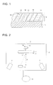
- a radiation image conversion panel of this invention is provided with support 11 and stimulable fluorescent substance layer 12 which as formed on said support 11 and contains a stimulable fluorescent substance, as shown in Fig. 1. Further, a protective layer (not shown in the drawing) is appropriately provided to protect stimulable fluorescent substance layer 12. Herein, in stimulable fluorescent substance layer 12, gaps 14 are formed between columnar crystals 13 of a stimulable fluorescent substance.
- the inventors of this invention have found that it is possible to make a sharpness distribution in the plane uniform and significantly improve image quality of a radiation image, by constituting stimulable fluorescent substance layer 12 of a columnar crystal structure as well as defining slopes D 1 and D 2 of columnar crystals at arbitrary two points in a radiation image conversion panel plane to satisfy 0 ° ⁇
- slopes D 1 and D 2 of columnar crystals into the above range is that the slope distribution shows variation resulting in a non-uniform sharpness distribution in the plane in the case of 40 ° ⁇
- each cross-section of the stimulable fluorescent substance layer with respect to arbitrary two points in a radiation image conversion panel plane is observed through an electronmicroscope (SEM) to determine the slopes.
- SEM electronmicroscope
- a support utilized in this invention can be selected from commonly known materials as conventional radiation image conversion panels, however, is preferably a quartz glass sheet, a metal sheet comprising such as aluminum, iron, tin and chromium or a carbon fiber reinforced sheet, in the case of a support for a fluorescent layer being formed by a gas phase deposition.
- a support is preferably provided with a resin layer to make the surface to be a smooth plane.
- a resin layer preferably contains a compound such as polyimide, polyethylene terephtalate, paraffin and graphite, and the thickness is preferably approximately 5 - 50 ⁇ m.
- the resin layer may be provided either on the front surface or the back surface, or on the both of them.
- a means to provide a resin layer on a support includes such as a lamination method and a coating method.
- a lamination method is performed by use of heating and pressing rollers, and the conditions are preferably heating at approximately 80 - 150 °C, pressing at 4.90 x 10 - 2.94 x 10 2 N/cm and a transport rate of 0.1 - 20 m/sec.
- a thickness of a stimulable fluorescent substance layer varies depending on the purposes of application of a radiation image conversion panel and types of a stimulable fluorescent substance, however, is 50 - 2000 ⁇ m, preferably 50 - 1000 ⁇ m and more preferably 100 - 800 ⁇ m, with respect to obtaining the effects of this invention.
- a stimulable fluorescent substance layer includes a stimulable fluorescent substance comprising an alkali halogenide represented by following general formula (1) as a mother material.
- General formula (1) M 1 X ⁇ aM 2 X' ⁇ bM 3 X" 3 : eA
- M 1 represents at least one type of an alkali metal selected from a group comprising Li, Na, K, Rb and Cs
- M 2 represents at least one type of an alkali metal selected from a group comprising Li, Na, K, Rb and Cs other than M 1
- M 3 represents at least one type of an tri-valent metal selected from a group comprising Y, La, Ce, Pr, Nd, Pm, Sm, Eu, Gd, Tb, Dy, Ho, Er, Tm, Yb and Lu
- X, X' and X" each represent at least one type of a halogen selected from a group comprising F, Cl, Br and I
- A represents at least one type of a rare earth element selected
- M 1 represents at least one type of an alkali metal selected from a group comprising each atom of Li, Na, K, Rb and Cs, among them preferably at least one type of an alkali earth metal atom selected from each atom of Rb and Cs and more preferably a Cs atom.
- M 2 represents at least one type of an alkali metal atom selected from a group comprising Li, Na, K, Rb and Cs other than M 1 , among them preferably at least one type of an alkali earth metal atom selected from each atom of Na, K and Rb.
- M 3 represents at least one type of an tri-valent metal selected from a group comprising Y, La, Ce, Pr, Nd, Pm, Sm, Eu, Gd, Tb, Dy, Ho, Er, Tm, Yb and Lu, among them preferably utilized is a tri-valent metal atom selected from each atom of Y, Ce, Sm, Eu, La, Gd and Lu.
- A represents at least one type of a rare earth element selected from Eu, Tb, In, Ce, Tm, Dy, Pr, Ho, Nd, Yb, Er, Gd, Lu, Sm and Y, among them preferable is a Eu atom.
- X, X' and X" each represent at least one type of a halogen atom selected from a group comprising each atom of F, Cl, Br and I, preferably a halogen atom selected from each atom of F, Cl and Br and more preferably a Br atom, with respect to improving stimulated emission luminance of a stimulable fluorescent substance.
- b value satisfies 0 ⁇ b ⁇ 0.5 and preferably 0 ⁇ b ⁇ 10 -2 .
- Stimulable fluorescent substances represented by general formula (1) are manufactured by a method described below.
- Fluorescent substance raw materials of aforesaid (a) - (c) are weighed to make a mixing composition having the aforesaid value range, and dissolved in pure water.
- they may be sufficiently mixed by utilizing such as a mortar, a ball mill or a mixer mill.
- the obtained raw material mixture is charged in a heat-resistant vessel such as a quartz crucible or an alumina crucible to be burned in an electric oven.
- the burning temperature is preferably 500 - 1000 °C.
- the burning time varies depending on the charging amount of raw materials and the burning temperature, however, is preferably 0.5 - 6 hours.
- the burning atmosphere is preferably a weakly reducing atmosphere such as a nitrogen gas atmosphere including a small amount of a hydrogen gas and carbon dioxide gas atmosphere including a small amount of carbon monoxide, a neutral atmosphere such as a nitrogen atmosphere and an argon gas atmosphere, or a weakly oxidizing atmosphere including a small amount of oxygen gas.
- a weakly reducing atmosphere such as a nitrogen gas atmosphere including a small amount of a hydrogen gas and carbon dioxide gas atmosphere including a small amount of carbon monoxide
- a neutral atmosphere such as a nitrogen atmosphere and an argon gas atmosphere
- a weakly oxidizing atmosphere including a small amount of oxygen gas.
- the burned product is taken out of an electric oven to be ground. Thereafter, the burned product powder may be filled in a heat-resistant vessel and charged into an electric oven to be burned again under the same burning conditions described above, which enables further enhancement of emission luminance of a stimulable fluorescent substance. Further, at the time of cooling the burned product from a burning temperature to room temperature, a desired stimulable fluorescent substance can be obtained by taking the burned product out of an electric oven to be cooled while being left in the air, however, it may be cooled while being kept in a weakly reducing atmosphere or in a neutral atmosphere which is the same condition as during burning.
- the burned product in a weakly reducing atmosphere, a neutral atmosphere or a weakly oxidizing atmosphere by transferring from a heating section to a cooling section inside an electric oven, because further enhancement of emission luminance at stimulation of the obtained stimulable fluorescent substance is possible.
- a stimulable fluorescent substance layer of this invention is formed by a gas phase accumulation method.
- a gas phase accumulation method of a stimulable fluorescent substance utilized can be an evaporation method, a spattering method, a CVD method, an ion plating method and others, however, specifically preferable in this invention is an evaporation method.
- evaporation equipment 1 is equipped with vacuum chamber 2, evaporation source 3 which is installed in said vacuum chamber 2 and evaporates a vapor on support 11, support holder 4 which holds support 11, support rotating mechanism 5 which rotates said support holder 4 against evaporation source 3 and evaporates a vapor from said evaporation source 3, and vacuum pump 6 which performs evacuation and introduction of the atmosphere inside vacuum chamber 2.
- Evaporation source 3 may be constituted of an alumina crucible wounded with a heater to contain and heat a stimulable fluorescent substance by means of a resistance heating method, of a boat, or of a heater comprising a high melting point metal.
- a method to heat a stimulable fluorescent substance may be one by means of electron beam or high frequency induction other than a resistance heating method, however, in this invention, preferable is a resistance heating method with respect to a relatively simple constitution and easy handling, being low-priced as well as applicability to great many substances.
- evaporation source 3 may be a molecular beam source by means of a molecular source epitaxial method.
- This evaporation source 3 is preferably arranged in vacuum chamber 2 so as to make an acute angle ⁇ 1 , formed by the plane direction of support 11 and the normal line which connects an arbitrary point in a unit evaporation region on support 11 and the center of an evaporation source 3, satisfy 50° ⁇ ⁇ 1 ⁇ 90°.
- the reason to define the acute angle ⁇ 1 to be 50° ⁇ ⁇ 1 ⁇ 90° is because
- Support rotation mechanism 5 is constituted of such as rotation axis 5a which supports support holder 4 as well as rotates support holder 4 and a motor (not shown in the drawing) which is arranged outside vacuum chamber 2 and works as a driving source of rotation axis 5a.
- support surface temperature controlling heater 7 which heats support 11 is installed in vacuum chamber 2.
- absorbed substances on the surface of support 11 can be released and eliminated, generation of an impurity layer between support 11 and a stimulable fluorescent substance can be prevented, and enhancement of adhesion and adjustment of layer properties of a stimulable fluorescent substance layer can be performed.
- a shutter (not shown in the drawing), which shut the space being spread from evaporation source to support 11, may be equipped between support 11 and evaporation source 3.
- the shutter can prevent substances other than the object substances, which are adhered on the surface of a stimulable fluorescent substance, from evaporating and being adhered on support 11 at the initial stage of evaporation.
- evaporation source 3 is arranged in vacuum chamber 2 so as to make an acute angle ⁇ 1 satisfy a desired acute angle ⁇ 1 within 50° ⁇ ⁇ 1 ⁇ 90°, and support 11 is attached to support holder 4.
- vacuum chamber 2 is evacuated.
- support holder 4 is rotated against evaporation source 3 by support rotation mechanism 5, and a stimulable fluorescent substance is evaporated from heated evaporation source 3 when vacuum chamber 2 reaches a vacuum degree at which evaporation is possible, to grow the stimulable fluorescent substance on the surface of support 11 up to a desired thickness.
- distance d1 between support 11 and evaporation source 3 is preferably arranged at 100 - 1500 mm.
- a stimulable fluorescent substance utilized as an evaporation source is preferably finished into a tablet form by means of pressure compression.
- a raw material thereof or a raw material mixture thereof is possible to be utilized.
- stimulable fluorescent layer 12 without containing a binder is formed as shown in Fig. 1, however, fillers such as a binder may be filled in gap 14 formed between columnar crystals 13, which reinforces stimulable fluorescent substance layer 12, in addition to this a high light absorptive substance or a high light reflective substance also may be filled. This can provide a reinforcement effect, as well as is effective to reduce a lateral light diffusion of exciting light for stimulation being incident into stimulable fluorescent substance layer 12.
- a stimulable fluorescent substance layer can be also formed by dividing into plural times. In addition to this, it is also possible to form a stimulable fluorescent layer simultaneously with synthesizing a stimulable fluorescent substance on a support.
- an object to be evaporated (a support, a protective layer or an intermediate layer) may be appropriately cooled or heated at the time of evaporation.
- a stimulable fluorescent layer may be heat processed.
- a reactive evaporation may be performed by appropriately introducing a gas such as O 2 and H 2 .
- a temperature of forming a stimulable fluorescent layer is preferably set at room temperature (rt) - 300 °C and more preferably at 50 - 200 °C.
- a radiation image conversion panel of this invention is manufactured by appropriately providing a protective layer on the opposite side to the support of a stimulable fluorescent substance layer after forming a stimulable fluorescent substance layer provided with a layer comprising a columnar crystal structure.
- a protective layer may be formed by directly coating a protective layer coating solution on the surface of a stimulable fluorescent susbstance layer, or by adhering a protective layer prepared separately in advance on a stimulable fluorescent substance layer.
- a protective layer As materials for a protective layer, utilized are ordinary protective layer materials such as cellulose acetate, nitro cellulose, polymethylmethacrylate, polyvinyl butyral, polyvinyl formal, polycarbonate, polyester, polyethylene terephthalate, polyethylene, polyvinylidene chloride, nylon, polytetrafluoroethylene, polytrifluorochloroethylene, a tetrafluoroethylene-hexafluoropropyrene copolymer, vinylidene chloride-vinyl chloride copolymer and a vinylidene chloride-acrylonitrile copolymer.
- a transparent glass substrate can be also utilized as a protective layer.
- the protective layer may be also formed by accumulating an inorganic substance such as SiC, Si02, SiN and Al 2 O 3 by such as an evaporation method or a spattering method. These protective layer preferably has a layer thickness of 0.1 - 2000 ⁇ m.
- a stimulable fluorescent substance layer having a columnar structure comprising a stimulable fluorescent substance (CsBr : Eu) was formed on the one side of a support utilizing evaporation equipment 1 shown in Fig. 2.
- CFPR support having a size of 500 mm x 500 mm was utilized.
- the above fluorescent substance raw material as an evaporation material was filled in a resistance heating crucible while support 11 was mounted on rotating support holder 4, and evaporation source 3 was arranged so as to make acute angle ⁇ 1 , which is formed by the plane direction of support 11 and a normal line connecting the center of support 11 and the center of evaporation source 3, of 50° as well as distance d1 between support 11 and evaporation source 3 was adjusted to 420 mm.
- a temperature of support 11 was kept at 100 °C while rotating support 11 at a rate of 10 rpm.
- a stimulable fluorescent substance was evaporated by heating the resistance heating crucible and evaporation was finished when a thickness of a stimulable fluorescent substance layer reached 400 ⁇ m.
- the stimulable fluorescent substance layer was put into a protective bag under a dry air atmosphere, resulting in preparation of a radiation image conversion panel having a structure comprising a stimulable fluorescent substance being sealed.
- a radiation image conversion panel was prepared in a similar manner to example 1, except that distance d1 between a support and an evaporation source was adjusted to 610 mm and acute angle ⁇ 1 to 60°.
- a radiation image conversion panel was prepared in a similar manner to example 1, except that distance d1 between a support and an evaporation source was adjusted to 970 mm and acute angle ⁇ 1 to 70°.
- a radiation image conversion panel was prepared in a similar manner to example 1, except that distance d1 between a support and an evaporation source was adjusted to 130 mm and acute angle ⁇ 1 to 20°.
- a radiation image conversion panel was prepared in a similar manner to example 1, except that distance d1 between a support and an evaporation source was adjusted to 205 mm and acute angle ⁇ 1 to 30°.
- a radiation image conversion panel was prepared in a similar manner to example 1, except that distance d1 between a support and an evaporation source was adjusted to 300 mm and acute angle ⁇ 1 to 40°.
- the radiation image conversion panel was excited by scanning with a semi-conductor laser (680 nm) of 100 mW, and a stimulated emission from a stimulable fluorescent substance layer was received with a photomultiplier tube (manufactured by Hamamatsu Photonics K.K.) to be converted to an electrical signal, which was analogue/digital converted and recorded on a magnetic tape.
- the recorded magnetic tape was analyzed by a computer to determine a modulation transfer function (MTF) value of an X-ray image recorded on a magnetic tape.
- the MTF was represented by a special frequency at 1 cycle (lines pair)/mm.
- Sharpness distribution (%) ⁇ MTF (Max. value) - MTF (Center value) ⁇ /MTF (Center value) x 100
- examples 1 - 3 in which slopes of columnar crystals at arbitrary two points in a radiation image conversion panel, D 1 and D 2 , satisfy 0° ⁇
Landscapes
- Chemical & Material Sciences (AREA)
- Engineering & Computer Science (AREA)
- Organic Chemistry (AREA)
- Materials Engineering (AREA)
- Mechanical Engineering (AREA)
- Metallurgy (AREA)
- Chemical Kinetics & Catalysis (AREA)
- Physics & Mathematics (AREA)
- General Engineering & Computer Science (AREA)
- High Energy & Nuclear Physics (AREA)
- Inorganic Chemistry (AREA)
- Conversion Of X-Rays Into Visible Images (AREA)
- Luminescent Compositions (AREA)
- Radiography Using Non-Light Waves (AREA)
- Physical Vapour Deposition (AREA)
Applications Claiming Priority (2)
| Application Number | Priority Date | Filing Date | Title |
|---|---|---|---|
| JP2003407338A JP2005164534A (ja) | 2003-12-05 | 2003-12-05 | 放射線像変換パネル及び放射線像変換パネルの製造方法 |
| JP2003407338 | 2003-12-05 |
Publications (2)
| Publication Number | Publication Date |
|---|---|
| EP1538636A2 true EP1538636A2 (de) | 2005-06-08 |
| EP1538636A3 EP1538636A3 (de) | 2007-08-22 |
Family
ID=34464023
Family Applications (1)
| Application Number | Title | Priority Date | Filing Date |
|---|---|---|---|
| EP04106108A Withdrawn EP1538636A3 (de) | 2003-12-05 | 2004-11-26 | Strahlungsbildwandler und Verfahren zu seiner Herstellung |
Country Status (3)
| Country | Link |
|---|---|
| US (1) | US7253421B2 (de) |
| EP (1) | EP1538636A3 (de) |
| JP (1) | JP2005164534A (de) |
Families Citing this family (1)
| Publication number | Priority date | Publication date | Assignee | Title |
|---|---|---|---|---|
| JP6030068B2 (ja) | 2011-12-16 | 2016-11-24 | 東芝電子管デバイス株式会社 | 放射線検出パネルの製造装置 |
Family Cites Families (15)
| Publication number | Priority date | Publication date | Assignee | Title |
|---|---|---|---|---|
| US4947046A (en) * | 1988-05-27 | 1990-08-07 | Konica Corporation | Method for preparation of radiographic image conversion panel and radiographic image conversion panel thereby |
| US5786600A (en) * | 1995-12-19 | 1998-07-28 | Eastman Kodak Company | (Barium hafnate:Ti, Ce, Pb) phosphors phosphor screens and phosphor preparation methods |
| US5693254A (en) * | 1996-06-28 | 1997-12-02 | Eastman Kodak Company | Cesium-zinc halide phosphors, phosphor screens, and preparation methods |
| EP0869533B1 (de) * | 1996-09-18 | 2003-11-19 | Kabushiki Kaisha Toshiba | Röntgenbildröhre und herstellungsverfahren für dieselbe |
| US6452203B1 (en) * | 1998-11-10 | 2002-09-17 | Agfa-Gevaert | Method for monitoring a dose of penetrating radiation absorbed by an object |
| US6396066B1 (en) * | 2000-09-21 | 2002-05-28 | Eastman Kodak Company | Image storage phosphor panels having flexible supports |
| US7022477B2 (en) * | 2001-05-18 | 2006-04-04 | Fuji Photo Film Co., Ltd. | Detection of target substances utilizing biochemically specific binding reaction |
| DE10234732A1 (de) * | 2001-07-30 | 2003-06-05 | Fuji Photo Film Co Ltd | Herstellung einer Strahlungsbild-Speicherplatte |
| JP2003050298A (ja) * | 2001-08-06 | 2003-02-21 | Fuji Photo Film Co Ltd | 放射線像変換パネルおよびその製造方法 |
| US6864491B2 (en) * | 2002-02-14 | 2005-03-08 | Konica Corporation | Radiation image conversion panel |
| US7091501B2 (en) * | 2002-03-08 | 2006-08-15 | Agfa-Gevaert | Binderless storage phosphor screen on a dedicated support |
| US6967339B2 (en) * | 2002-03-26 | 2005-11-22 | Agfa-Gevaert | Needle-shaped cylindrical storage phosphor crystals |
| US6921909B2 (en) * | 2002-08-27 | 2005-07-26 | Radiation Monitoring Devices, Inc. | Pixellated micro-columnar films scintillator |
| US7057200B2 (en) * | 2003-07-24 | 2006-06-06 | Eastman Kodak Company | Storage phosphor erase |
| JP2006271700A (ja) * | 2005-03-29 | 2006-10-12 | Fuji Photo Film Co Ltd | 放射線像変換パネルおよび放射線画像診断システム |
-
2003
- 2003-12-05 JP JP2003407338A patent/JP2005164534A/ja active Pending
-
2004
- 2004-11-26 EP EP04106108A patent/EP1538636A3/de not_active Withdrawn
- 2004-11-30 US US10/999,689 patent/US7253421B2/en not_active Expired - Fee Related
Also Published As
| Publication number | Publication date |
|---|---|
| JP2005164534A (ja) | 2005-06-23 |
| US20050121622A1 (en) | 2005-06-09 |
| EP1538636A3 (de) | 2007-08-22 |
| US7253421B2 (en) | 2007-08-07 |
Similar Documents
| Publication | Publication Date | Title |
|---|---|---|
| EP2261303B1 (de) | Strahlungsbildwandler und Verfahren zu seiner Herstellung | |
| JP2005106682A (ja) | 放射線像変換パネル及び放射線像変換パネルの製造方法 | |
| US6864491B2 (en) | Radiation image conversion panel | |
| JP2006113007A (ja) | 放射線画像変換パネル | |
| US7253421B2 (en) | Radiation image conversion panel and manufacturing method thereof | |
| EP1526553B1 (de) | Strahlungsbildwandler | |
| EP1517340B1 (de) | Strahlungsbildwandler und Verfahren zu seiner Herstellung | |
| JP3952012B2 (ja) | 放射線像変換パネル及び放射線像変換パネルの製造方法 | |
| US7081333B2 (en) | Radiation image conversion panel and preparation method thereof | |
| JP4345460B2 (ja) | 放射線像変換パネル | |
| JP2006090851A (ja) | 放射線画像変換パネルの製造装置及び放射線画像変換パネルの製造方法 | |
| JP2005091146A (ja) | 放射線像変換パネル及び放射線像変換パネルの製造方法 | |
| JP3997978B2 (ja) | 放射線画像変換パネル | |
| JP2005098717A (ja) | 放射線像変換パネル及び放射線像変換パネルの製造方法 | |
| EP1518914A2 (de) | Strahlungsbildwandler und Verfahren zu seiner Herstellung | |
| JP4830280B2 (ja) | 放射線画像変換パネルの製造装置及び放射線画像変換パネルの製造方法 | |
| JP2006010617A (ja) | 放射線変換パネルの製造方法とその製造装置 | |
| JP5136662B2 (ja) | 放射線画像変換パネルの製造装置及び放射線画像変換パネルの製造方法 | |
| JP2005098716A (ja) | 放射線像変換パネル及び放射線像変換パネルの製造方法 | |
| JP2005106770A (ja) | 放射線像変換パネル及び放射線像変換パネルの製造方法 | |
| JP2004212189A (ja) | 放射線画像変換パネル及び放射線画像変換パネルの製造方法 | |
| JP2005106771A (ja) | 放射線像変換パネル及び放射線像変換パネルの製造方法 | |
| JP2005164535A (ja) | 放射線像変換パネル | |
| JP2005114721A (ja) | 放射線画像変換パネルおよび放射線画像変換パネルの製造方法 | |
| JP2006152199A (ja) | 放射線画像変換パネル、その製造方法及び製造装置 |
Legal Events
| Date | Code | Title | Description |
|---|---|---|---|
| PUAI | Public reference made under article 153(3) epc to a published international application that has entered the european phase |
Free format text: ORIGINAL CODE: 0009012 |
|
| AK | Designated contracting states |
Kind code of ref document: A2 Designated state(s): AT BE BG CH CY CZ DE DK EE ES FI FR GB GR HU IE IS IT LI LU MC NL PL PT RO SE SI SK TR |
|
| AX | Request for extension of the european patent |
Extension state: AL HR LT LV MK YU |
|
| PUAL | Search report despatched |
Free format text: ORIGINAL CODE: 0009013 |
|
| AK | Designated contracting states |
Kind code of ref document: A3 Designated state(s): AT BE BG CH CY CZ DE DK EE ES FI FR GB GR HU IE IS IT LI LU MC NL PL PT RO SE SI SK TR |
|
| AX | Request for extension of the european patent |
Extension state: AL HR LT LV MK YU |
|
| RIC1 | Information provided on ipc code assigned before grant |
Ipc: C23C 14/50 20060101ALI20070719BHEP Ipc: G21K 4/00 20060101AFI20050419BHEP |
|
| RIN1 | Information on inventor provided before grant (corrected) |
Inventor name: MAEZAWA, AKIHIROIKONICA MINOLTA MED.&GRAPHIC INC Inventor name: YANAGITA, TAKAFUMIKONICA MINOLTA MED.&GRAPHICINC Inventor name: MISHINA, NORIYUKIKONICA MINOLTA MED.&GRAPHIC INC |
|
| RAP1 | Party data changed (applicant data changed or rights of an application transferred) |
Owner name: KONICA MINOLTA MEDICAL & GRAPHIC, INC. |
|
| 17P | Request for examination filed |
Effective date: 20080130 |
|
| AKX | Designation fees paid |
Designated state(s): DE FR GB |
|
| 17Q | First examination report despatched |
Effective date: 20080721 |
|
| STAA | Information on the status of an ep patent application or granted ep patent |
Free format text: STATUS: THE APPLICATION IS DEEMED TO BE WITHDRAWN |
|
| 18D | Application deemed to be withdrawn |
Effective date: 20100601 |