EP1536673B1 - Composite multi-layer substrate and module using the substrate - Google Patents
Composite multi-layer substrate and module using the substrate Download PDFInfo
- Publication number
- EP1536673B1 EP1536673B1 EP03733093.3A EP03733093A EP1536673B1 EP 1536673 B1 EP1536673 B1 EP 1536673B1 EP 03733093 A EP03733093 A EP 03733093A EP 1536673 B1 EP1536673 B1 EP 1536673B1
- Authority
- EP
- European Patent Office
- Prior art keywords
- core member
- electronic component
- resin layer
- layer
- side resin
- Prior art date
- Legal status (The legal status is an assumption and is not a legal conclusion. Google has not performed a legal analysis and makes no representation as to the accuracy of the status listed.)
- Expired - Lifetime
Links
Images






Classifications
-
- H—ELECTRICITY
- H05—ELECTRIC TECHNIQUES NOT OTHERWISE PROVIDED FOR
- H05K—PRINTED CIRCUITS; CASINGS OR CONSTRUCTIONAL DETAILS OF ELECTRIC APPARATUS; MANUFACTURE OF ASSEMBLAGES OF ELECTRICAL COMPONENTS
- H05K1/00—Printed circuits
- H05K1/18—Printed circuits structurally associated with non-printed electric components
- H05K1/182—Printed circuits structurally associated with non-printed electric components associated with components mounted in printed circuit boards [PCB], e.g. insert-mounted components [IMC]
- H05K1/185—Printed circuits structurally associated with non-printed electric components associated with components mounted in printed circuit boards [PCB], e.g. insert-mounted components [IMC] associated with components encapsulated in the insulating substrate of the PCBs; associated with components incorporated in internal layers of multilayer circuit boards
-
- H—ELECTRICITY
- H05—ELECTRIC TECHNIQUES NOT OTHERWISE PROVIDED FOR
- H05K—PRINTED CIRCUITS; CASINGS OR CONSTRUCTIONAL DETAILS OF ELECTRIC APPARATUS; MANUFACTURE OF ASSEMBLAGES OF ELECTRICAL COMPONENTS
- H05K1/00—Printed circuits
- H05K1/02—Details
- H05K1/0201—Thermal arrangements, e.g. for cooling, heating or preventing overheating
- H05K1/0203—Cooling of mounted components
- H05K1/021—Components thermally connected to metal substrates or heat-sinks by insert mounting
-
- H—ELECTRICITY
- H10—SEMICONDUCTOR DEVICES; ELECTRIC SOLID-STATE DEVICES NOT OTHERWISE PROVIDED FOR
- H10W—GENERIC PACKAGES, INTERCONNECTIONS, CONNECTORS OR OTHER CONSTRUCTIONAL DETAILS OF DEVICES COVERED BY CLASS H10
- H10W70/00—Package substrates; Interposers; Redistribution layers [RDL]
- H10W70/01—Manufacture or treatment
- H10W70/05—Manufacture or treatment of insulating or insulated package substrates, or of interposers, or of redistribution layers
- H10W70/08—Manufacture or treatment of insulating or insulated package substrates, or of interposers, or of redistribution layers by depositing layers on the chip or wafer, e.g. "chip-first" RDLs
- H10W70/09—Manufacture or treatment of insulating or insulated package substrates, or of interposers, or of redistribution layers by depositing layers on the chip or wafer, e.g. "chip-first" RDLs extending onto an encapsulation that laterally surrounds the chip or wafer, e.g. fan-out wafer level package [FOWLP] RDLs
-
- H—ELECTRICITY
- H10—SEMICONDUCTOR DEVICES; ELECTRIC SOLID-STATE DEVICES NOT OTHERWISE PROVIDED FOR
- H10W—GENERIC PACKAGES, INTERCONNECTIONS, CONNECTORS OR OTHER CONSTRUCTIONAL DETAILS OF DEVICES COVERED BY CLASS H10
- H10W70/00—Package substrates; Interposers; Redistribution layers [RDL]
- H10W70/01—Manufacture or treatment
- H10W70/05—Manufacture or treatment of insulating or insulated package substrates, or of interposers, or of redistribution layers
- H10W70/093—Connecting or disconnecting other interconnections thereto or therefrom, e.g. connecting bond wires or bumps
-
- H—ELECTRICITY
- H10—SEMICONDUCTOR DEVICES; ELECTRIC SOLID-STATE DEVICES NOT OTHERWISE PROVIDED FOR
- H10W—GENERIC PACKAGES, INTERCONNECTIONS, CONNECTORS OR OTHER CONSTRUCTIONAL DETAILS OF DEVICES COVERED BY CLASS H10
- H10W70/00—Package substrates; Interposers; Redistribution layers [RDL]
- H10W70/60—Insulating or insulated package substrates; Interposers; Redistribution layers
- H10W70/611—Insulating or insulated package substrates; Interposers; Redistribution layers for connecting multiple chips together
- H10W70/614—Insulating or insulated package substrates; Interposers; Redistribution layers for connecting multiple chips together the multiple chips being integrally enclosed
-
- H—ELECTRICITY
- H10—SEMICONDUCTOR DEVICES; ELECTRIC SOLID-STATE DEVICES NOT OTHERWISE PROVIDED FOR
- H10W—GENERIC PACKAGES, INTERCONNECTIONS, CONNECTORS OR OTHER CONSTRUCTIONAL DETAILS OF DEVICES COVERED BY CLASS H10
- H10W70/00—Package substrates; Interposers; Redistribution layers [RDL]
- H10W70/60—Insulating or insulated package substrates; Interposers; Redistribution layers
- H10W70/67—Insulating or insulated package substrates; Interposers; Redistribution layers characterised by their insulating layers or insulating parts
- H10W70/68—Shapes or dispositions thereof
- H10W70/685—Shapes or dispositions thereof comprising multiple insulating layers
-
- H—ELECTRICITY
- H05—ELECTRIC TECHNIQUES NOT OTHERWISE PROVIDED FOR
- H05K—PRINTED CIRCUITS; CASINGS OR CONSTRUCTIONAL DETAILS OF ELECTRIC APPARATUS; MANUFACTURE OF ASSEMBLAGES OF ELECTRICAL COMPONENTS
- H05K2201/00—Indexing scheme relating to printed circuits covered by H05K1/00
- H05K2201/09—Shape and layout
- H05K2201/09209—Shape and layout details of conductors
- H05K2201/09654—Shape and layout details of conductors covering at least two types of conductors provided for in H05K2201/09218 - H05K2201/095
- H05K2201/0969—Apertured conductors
-
- H—ELECTRICITY
- H05—ELECTRIC TECHNIQUES NOT OTHERWISE PROVIDED FOR
- H05K—PRINTED CIRCUITS; CASINGS OR CONSTRUCTIONAL DETAILS OF ELECTRIC APPARATUS; MANUFACTURE OF ASSEMBLAGES OF ELECTRICAL COMPONENTS
- H05K2201/00—Indexing scheme relating to printed circuits covered by H05K1/00
- H05K2201/09—Shape and layout
- H05K2201/09209—Shape and layout details of conductors
- H05K2201/09654—Shape and layout details of conductors covering at least two types of conductors provided for in H05K2201/09218 - H05K2201/095
- H05K2201/09745—Recess in conductor, e.g. in pad or in metallic substrate
-
- H—ELECTRICITY
- H05—ELECTRIC TECHNIQUES NOT OTHERWISE PROVIDED FOR
- H05K—PRINTED CIRCUITS; CASINGS OR CONSTRUCTIONAL DETAILS OF ELECTRIC APPARATUS; MANUFACTURE OF ASSEMBLAGES OF ELECTRICAL COMPONENTS
- H05K3/00—Apparatus or processes for manufacturing printed circuits
- H05K3/44—Manufacturing insulated metal core circuits or other insulated electrically conductive core circuits
- H05K3/445—Manufacturing insulated metal core circuits or other insulated electrically conductive core circuits having insulated holes or insulated via connections through the metal core
-
- H—ELECTRICITY
- H05—ELECTRIC TECHNIQUES NOT OTHERWISE PROVIDED FOR
- H05K—PRINTED CIRCUITS; CASINGS OR CONSTRUCTIONAL DETAILS OF ELECTRIC APPARATUS; MANUFACTURE OF ASSEMBLAGES OF ELECTRICAL COMPONENTS
- H05K3/00—Apparatus or processes for manufacturing printed circuits
- H05K3/46—Manufacturing multilayer circuits
- H05K3/4611—Manufacturing multilayer circuits by laminating two or more circuit boards
- H05K3/4641—Manufacturing multilayer circuits by laminating two or more circuit boards having integrally laminated metal sheets or special power cores
-
- H—ELECTRICITY
- H10—SEMICONDUCTOR DEVICES; ELECTRIC SOLID-STATE DEVICES NOT OTHERWISE PROVIDED FOR
- H10W—GENERIC PACKAGES, INTERCONNECTIONS, CONNECTORS OR OTHER CONSTRUCTIONAL DETAILS OF DEVICES COVERED BY CLASS H10
- H10W70/00—Package substrates; Interposers; Redistribution layers [RDL]
- H10W70/099—Connecting interconnections to insulating or insulated package substrates, interposers or redistribution layers
-
- H—ELECTRICITY
- H10—SEMICONDUCTOR DEVICES; ELECTRIC SOLID-STATE DEVICES NOT OTHERWISE PROVIDED FOR
- H10W—GENERIC PACKAGES, INTERCONNECTIONS, CONNECTORS OR OTHER CONSTRUCTIONAL DETAILS OF DEVICES COVERED BY CLASS H10
- H10W70/00—Package substrates; Interposers; Redistribution layers [RDL]
- H10W70/60—Insulating or insulated package substrates; Interposers; Redistribution layers
-
- H—ELECTRICITY
- H10—SEMICONDUCTOR DEVICES; ELECTRIC SOLID-STATE DEVICES NOT OTHERWISE PROVIDED FOR
- H10W—GENERIC PACKAGES, INTERCONNECTIONS, CONNECTORS OR OTHER CONSTRUCTIONAL DETAILS OF DEVICES COVERED BY CLASS H10
- H10W70/00—Package substrates; Interposers; Redistribution layers [RDL]
- H10W70/60—Insulating or insulated package substrates; Interposers; Redistribution layers
- H10W70/67—Insulating or insulated package substrates; Interposers; Redistribution layers characterised by their insulating layers or insulating parts
- H10W70/68—Shapes or dispositions thereof
- H10W70/682—Shapes or dispositions thereof comprising holes having chips therein
-
- H—ELECTRICITY
- H10—SEMICONDUCTOR DEVICES; ELECTRIC SOLID-STATE DEVICES NOT OTHERWISE PROVIDED FOR
- H10W—GENERIC PACKAGES, INTERCONNECTIONS, CONNECTORS OR OTHER CONSTRUCTIONAL DETAILS OF DEVICES COVERED BY CLASS H10
- H10W72/00—Interconnections or connectors in packages
- H10W72/071—Connecting or disconnecting
- H10W72/073—Connecting or disconnecting of die-attach connectors
-
- H—ELECTRICITY
- H10—SEMICONDUCTOR DEVICES; ELECTRIC SOLID-STATE DEVICES NOT OTHERWISE PROVIDED FOR
- H10W—GENERIC PACKAGES, INTERCONNECTIONS, CONNECTORS OR OTHER CONSTRUCTIONAL DETAILS OF DEVICES COVERED BY CLASS H10
- H10W72/00—Interconnections or connectors in packages
- H10W72/851—Dispositions of multiple connectors or interconnections
- H10W72/874—On different surfaces
-
- H—ELECTRICITY
- H10—SEMICONDUCTOR DEVICES; ELECTRIC SOLID-STATE DEVICES NOT OTHERWISE PROVIDED FOR
- H10W—GENERIC PACKAGES, INTERCONNECTIONS, CONNECTORS OR OTHER CONSTRUCTIONAL DETAILS OF DEVICES COVERED BY CLASS H10
- H10W72/00—Interconnections or connectors in packages
- H10W72/90—Bond pads, in general
- H10W72/941—Dispositions of bond pads
- H10W72/9413—Dispositions of bond pads on encapsulations
-
- H—ELECTRICITY
- H10—SEMICONDUCTOR DEVICES; ELECTRIC SOLID-STATE DEVICES NOT OTHERWISE PROVIDED FOR
- H10W—GENERIC PACKAGES, INTERCONNECTIONS, CONNECTORS OR OTHER CONSTRUCTIONAL DETAILS OF DEVICES COVERED BY CLASS H10
- H10W74/00—Encapsulations, e.g. protective coatings
-
- H—ELECTRICITY
- H10—SEMICONDUCTOR DEVICES; ELECTRIC SOLID-STATE DEVICES NOT OTHERWISE PROVIDED FOR
- H10W—GENERIC PACKAGES, INTERCONNECTIONS, CONNECTORS OR OTHER CONSTRUCTIONAL DETAILS OF DEVICES COVERED BY CLASS H10
- H10W90/00—Package configurations
- H10W90/701—Package configurations characterised by the relative positions of pads or connectors relative to package parts
- H10W90/731—Package configurations characterised by the relative positions of pads or connectors relative to package parts of die-attach connectors
- H10W90/734—Package configurations characterised by the relative positions of pads or connectors relative to package parts of die-attach connectors between a chip and a stacked insulating package substrate, interposer or RDL
-
- H—ELECTRICITY
- H10—SEMICONDUCTOR DEVICES; ELECTRIC SOLID-STATE DEVICES NOT OTHERWISE PROVIDED FOR
- H10W—GENERIC PACKAGES, INTERCONNECTIONS, CONNECTORS OR OTHER CONSTRUCTIONAL DETAILS OF DEVICES COVERED BY CLASS H10
- H10W90/00—Package configurations
- H10W90/701—Package configurations characterised by the relative positions of pads or connectors relative to package parts
- H10W90/731—Package configurations characterised by the relative positions of pads or connectors relative to package parts of die-attach connectors
- H10W90/736—Package configurations characterised by the relative positions of pads or connectors relative to package parts of die-attach connectors between a chip and a stacked lead frame, conducting package substrate or heat sink
Definitions
- This invention relates to a composite multi-layer substrate andmoduleusinga substrate designedtomake high density mounting of electronic components feasible.
- a mounting method using embedded mounting of the electronic components in a substrate (more specifically, not only the substrate face) but also the inner section of the substrate attracts attention.
- the electronic components are mounted in the front surface of the organic substrate serving as the core (hereinafter "core substrate”).
- core substrate a structure which encapsulates electronic components in a dielectric (nonconductive) prepreg resin is known (hereinafter “first prior art example”).
- second prior art example a structure in which grooves are formed in an organic system substrate wherein electronic components are embedded.
- a structure (hereinafter "third prior art example") in which holes corresponding to the size of electronic components are drilled in the prepreg and the electronic components are inserted and embedded in the holes of the prepreg when multi-layering or a structure (hereinafter “fourth prior art example”) with embedded sintered components by transfer in organic resin are known.
- the first prior art example and the fourth prior art example have a drawback of being disadvantageous to thin-sizing the substrate. Also, in the second prior art example and the third prior art example, there is a drawback mentioned which involves the processing cost of the grooves or holes. Moreover, because electronic component heat dissipation countermeasures are not entirely taken into consideration, any of the prior art examples (first through fourth prior art examples) have a drawback causing inconvenience in mounting electronic components especially in regard to heat generation in larger semiconductor chips, etc.
- Japanese Laid-Open Patent Application (Kokai) (A) No. S54-008871 (1979 ) titled “SEMICONDUCTOR DEVICE” discloses that in order to provide a solid electronic clock that is thin-shaped and a small size, while forming a pattern in one side of a printed circuit board, the device is made of a printed circuit board and a semiconductor chip of almost the equivalent thickness by adhering a metal plate to the rear surface, forming a "hole” in one or both directions in the pattern or metal plate and mounting a semiconductor chip in the hole.
- this prior art example when performing a resin seal of the semiconductor chip and multi-layering, there is a drawback of having to grind off the excess resin requiring additional work and making manufacturing costs more expensive.
- mounting in a hole and electronic component having multiple electrodes, such as the five-sided electrode, etc. there is a drawback that the type of electronic component which can be mounted has limitations and this constitution was not taken into consideration at all.
- Japanese Laid-Open Patent Application (Kokai) (A) No. S61-287194 (1986 ) titled "CHIP CARRIER FOR USE IN ELECTRONIC DEVICES” discloses elevation of the heat dissipation effect in electronic components.
- An insulating resin is laminated on a metal core front surface of a printed circuit board with a metal core base. While forming "concave portions" which reach to the metal core of that insulating resin, the device uses the metal core as a heat sink by mounting in the concave portions in order for the rear surface of an electronic component to be in contact to the metal core.
- This prior art example describes concave portions that are formed so the insulating resin laminated to the metal core rear surface (opposite side of the mounting surface of the electronic components) also reaches the metal core and the heat dissipation effect is elevated.
- Japanese Laid-Open Patent Application (Kokai) (A) No. S64-011400 (1989 ) titled "MULTILAYERED PLATE FOR MOUNTING IC CHIP” discloses a means to dissipate the heat of semiconductor chips from adjacent positions and to provide a multi-layer substrate for mounting semiconductor chips without generating improper bonding with the metal plate for heat dissipation by way of "holes" for semiconductor chip mounting formed in metal foil or a metal sheet.
- a printed circuit board is used in which the wiring network containing the above-mentioned holes are formed in one side or both sides of a metal base copper clad laminate inwhichprepregor copper foil is superimposed.
- the relationship between the metal foil in the side walls of the holes for mounting semiconductor chips or the height of the metal sheet and the thickness of the semiconductor chips is not defined.
- the configuration having taken into consideration heat dissipation of the semiconductor chips is not defined.
- consideration of thin-sizing is regarded to be insufficient.
- the increased manufacturing cost is readily anticipated.
- Japanese Laid-Open Patent Application (Kokai) (A) No. S64-012598 (1989 ) titled "IC CHIP MOUNTING MULTILAYER BOARD” discloses the use of a metal sheet with a thickness of 0 .1 ⁇ 1. 0mm, preferably 0.2 ⁇ 0.5mm, and with a thermal expansion coefficient of not more than 9x10 -6 cm/cm/°C. Although performing surface treatment suitably and improving the adhesive property is mentioned, these can also be considered similar problems (namely, consideration of thin-shaping is insufficient and increased manufacturing cost) relative to the seventh prior art example.
- Japanese Laid-Open Patent Application (Kokai) (A) No. H02-122534 (1990 ) titled "HYBRID INTEGRATED CIRCUIT” discloses a means to provide a hybrid integrated circuit in which high current can flow and miniaturized high density mounting is made possible.
- the wiring pattern is formed with "openings" for mounting semiconductor chips in a thermoplastic resin plate, and further consists of semiconductor chips and a metal plate of the same thickness arranged on either side of the semiconductor chips.
- the thermoplastic resin plate in which the wiring layer is formed in a multi-layer is united with another thermoplastic resin plate by means of thermocompression bonding.
- the lead terminals of the semiconductor chips are inserted in the openings provided between the thermoplastic resin plates formed in the multi-layer wiring layer and electrically connects with the wiring layer.
- the measures relative to heat dissipation of the semiconductor chips are not clear.
- the resin seal around the circumference of the semiconductor chips is problematic from thermocompression bonding with the thermoplastic resin plates in which the openings are formed and the thermoplastic resin plates with which the multi-layer wiring layer is formed.
- thermocompression bonding is performed in the state of fusing the thermoplastic resin plates, fluctuation of the thickness between layers of the section which forms the multi-layer wiring layer can be anticipated, and electrical specification control can be presumed to be difficult.
- FIG. 12A is a cross sectional plan view of the composite multi-layer substrate described in the official gazette.
- This composite multi-layer substrate 1 has a stacked multi-layer structure of a plurality of layers.
- the illustrated example has four layers (described later "resin layers") 2 ⁇ 5 which are composed of resin material.
- These resin layers 2 ⁇ 5 are common in that all use resin materials, such as epoxy, etc., for the material (so-called glass cloth 7) and only the layer of the resin layer 2 (drawing top layer) is different in the respect that a glass fiber 6 is contained within the braided (knitted) shape of a net as shown in FIG. 12B .
- the glass cloth 7 is reinforcement for enhancing the physical strength of the composite multi-layer substrate 1.
- the resin layer 2 which "has" the glass cloth 7 is denoted as "glass cloth layer 2”
- the resin layers 3 ⁇ 5 which "do not have” the glass cloth 7 are denoted as "glass clothless layers 3-5.”
- this composite multi-layer substrate 1 is bonded to copper foil on the bottommost surface (underside of the glass clothless layer 5) as the mounting side.
- the conductor pattern of copper foil is created by etching techniques, and the conductor pattern 8 of the required shape is formed.
- some of the glass cloth layer 2 is eliminated wherein a concavity 9 (It is called a mold cavity whereas an opening is generally closed.) is formed and the electronic components 10 (for example, semiconductor chips) are mounted in the concavity 9.
- the electronic components 10 are embedded" by using the inner section of the composite multi-layer substrate 1. Accordingly, other components can be mounted to the composite multi-layer substrate 1 front surface along with components mounted in higher density.
- JP 2001 298273 A relates to a mounting substrate incorporating electronic parts and a semiconductor package using the same.
- JP 06 140461 A relates to a mounting method and structure for semiconductor chip.
- the present invention's purpose is to prevent deterioration of the electrical characteristic accompanying the generation of migration and aiming at reduction of the manufacturing cost by using other reinforcement as a substitute for the glass cloth.
- the invention is defined in claim 1 and 2.
- the present invention has been made in view of the conventional prior art drawbacks mentioned above.
- the present invention is constituted with a composite multi-layer substrate comprising a flat plate-like core member formed of a material having excellent electric conductivity, excellent heat conductivity and high rigidity; a front side resin layer and a rear side resin layer covering at least a front surface and a rear surface of the core member; and a bottomless hole formed in the core member penetrates the front and rear of the core member, wherein an electronic component is mounted in the bottomless hole.
- the present invention is constituted with a composite multi-layer substrate comprising a flat plate-like core member formed of a material having excellent electrical conductivity, excellent heat conductivity and high rigidity; a front side resin layer and a rear side resin layer covering
- the present invention is not limited in particular. What is essential is just to have a combination of the three above-stated properties: "material which has excellent electrical conductivity, excellent heat conductivity and high rigidity.”
- the core member consists of"materialwhich has excellent electrical conductivity, excellent heat conductivity and high rigidity," typically, a core member made from metal (metallic) is preferred, but copper, Alloy 42, Invar, etc. are particularly preferred.
- each "bottomless hole” and “bottomed hole” are used to mount an electronic component (an electronic component is a general term of a passive component part, such as a semiconductor chip, a transistor, a resistance element, a capacitative element, an inductance element or other electronic components), the first is different in terms of a “a hole without a bottom (or a through hole) " and the latter "a hole with a bottom (or a concave portion)".
- the opening shape of a “bottomless hole” and a “bottomed hole” should just have an appropriate shape (for example, a little higher shape than the outside of the electronic component) which can conveniently mount a target electronic component.
- the composite multi-layer substrate further comprises a side surface resin material which covers the side surfaces of the core member; and the core member is entirely covered by the side surface resin material, the front side resin layer and the rear side resin layer.
- the composite multi-layer substrate comprises a column segment which divides the structure of the core member and penetrates the front and rear surfaces in the thickness direction of the core member; and the column segment is used as part of the electrical signal transmission path or power supply voltage transmission path to the direction of the front and rear surfaces of the substrate.
- the core member is used as a heat dissipation path of an electronic component through the inner wall of the bottomless hole or the flat bottomed hole when an electronic component is mounted in the bottomless hole or the flat bottomed hole.
- the composite multi-layer substrate wherein the upper surface height position of an electronic component after mounting in the bottomless hole or the bottomed hole, at least, does not cross the upper surface height position of the core member.
- the composite multi-layer substrate wherein a height size adjustment member is interposed between the bottom of an electronic component when an electronic component height size is lower than the depth size of the core member mounted in the bottomless hole; and the height size adjustment member performs mounting height adjustment of an electronic component.
- the composite multi-layer substrate wherein the height size adjustment member constitutes material which has heat conductivity.
- a module is constituted using the composite multi-layer substrate.
- FIGs. 1A-1C are main cross sectional plan views and a main perspective view of a composite multi-layer substrate in the form of the embodiment.
- the composite multi-layer substrate 20 has a "multi-layer structure.
- the composite multi-layer substrate 20 has a three-layer structure comprising a core member 21, a resin layer 22 (hereinafter “substrate front side resin layer”) and a resin layer 23 (hereinafter “substrate rear side resin layer. "
- the core member 21 in the shape of a flat plate-like board is composed of a material which has excellent electrical conductivity, excellent heat conductivity and high rigidity.
- the substrate front side resin layer 22 covers the front surface of the core member 21 (in the direction of the drawing, the upper surface).
- the substrate rear side resin layer 23 covers the rear surface of the core member 21 (in the direction of the drawing, the lower surface).
- the essential physical characteristics for the core member 21 are the above-mentioned three: excellent electrical conductivity, excellent heat conductivity and high rigidity.
- "Excellent electrical conductivity” pertains to the property of a material that allows electricity to pass through easily (that is, electrical resistance is low).
- “Excellent thermal conductivity” pertains to the ability to convey heat easily (that is, thermal conductivity is high).
- “High rigidity” pertains to minimal stress deformations due to bending or compressing.
- the construction material is not limited. What is essential is just to have the above-mentioned physical characteristics. Typically, metal (metallic) is preferred and especially more preferable when metals such as Cu (copper), Alloy 42, Invar, etc., are used which simultaneously satisfy the above-mentioned three physical characteristics.
- the material of the resin layers (the substrate front side resin layer 22 and the substrate rear side resin layer 23) covering the front and rear of the core member 21 has electrical insulating and environmental capabilities (water resistant, acid resistant, etc.), and if required further has the necessary dielectric constant.
- An insulating material for example, such as epoxy, polyimide, cyanate ester, Teflon (registered trademark), etc., used for a resin material or printed circuit boards can be used.
- a through hole 24 (hereinafter “bottomless hole”) of predetermined opening shape is formed in the core member 21 and penetrates the front and rear (refer to FIGs. 1A and 1B ).
- the bottomless hole 24 is used as a mounting hole of an electronic component 25.
- an electronic component 25 is mounted (embedded) in the inner part of the composite multi-layer substrate 20 and improvement of high density packaging can be achieved.
- the composite multi-layer substrate 20 which has such a structure, physical strength (flexural rigidity, etc.) of the composite multi-layer substrate 20 can be acquired with the rigidity of the core member 21. Therefore, the reinforcing material (glass cloth 7; refer to FIG. 12 ) used in the past can be made redundant and various inconveniences related to the application of the glass cloth can be avoided.
- the core member 21 which has "high rigidity” at least uses other reinforcement material which replaces the glass cloth
- the problem of ion migration explained earlier [Ion migration occurs relative to the interface of the glass fiber 6 front surface and the resin, whereby the insulation becomes destroyed and the electrical characteristic is deteriorated.]
- the problem of increased manufacturing cost [In order to form a bottomed hole 9 for a cavity, it is necessary to physically remove a portion of the resin layer 2. In that case, even though the inner part glass fiber 6 of resin layer 2 must be severed and such a cutting operation uses a precision processing apparatus, for example generally a laser, etc., a truncation error cannot be denied and considerable work hours are required.
- an electronic component mounting hole does not necessarily have to be a hole (namely, a bottomless hole) which "penetrates front and rear.”
- a concave portion 26 (hereinafter “flat bottomed hole”) may be formed in the core member 21 and an electronic component 25 can be mounted in a bottomed hole 26.
- the core member 21 can be used for heat dissipation of an electronic component 25.
- the resin layer structure (selection, thickness, etc.) for the front and rear surface sides of the core member 21 be approximately the same.
- the composite multi-layer substrate 20 front and rear surfaces are made into a symmetrical structure. Because the resin layers on the front and rear surface sides (front side resin layer 22 and rear side resin layer 23) of the core member 21 lessen differential thermal expansion, "curvature" of the composite multi-layer substrate 20 can be controlled.
- the front and rear surface sides of the core member 21 are each covered by the front side resin layer 22 and the rear side resin layer 23, it is desirable when the sides of the core member 21 are also covered by resin, etc. That is, it is desirable to completely enclose (sealant or coating) "all the surfaces" of the core member 21 with an environmentally resistant material equivalent to resin or thereto. Since the front and rear surfaces of the core member 21 each covered by the front side resin layer 22 and the rear side resin layer 23 are not unprotected to ambient air, there is no concern about oxidation. However, when the sides of the core member 21 are exposed, there is a possibility that the surfaces may oxidize gradually and generate an electrical short circuit, etc. causing a malfunction between the mounted components adjoining this exposure.
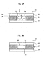
- FIGs. 2A and 2B are composition diagrams when mounting an electronic component 25 in a bottomless hole 24 of the core member 21.
- the upper surface height position La of the core member 21 constitutes a position always higher than the upper surface height position Lb of an electronic component 25, it can respond to the loading (load added when the front side resin layer 22, etc. is laminated) to an electronic component 25 on the core member 21 at the time of manufacturing the composite multi-layer substrate 20 and damage to an electronic component 25 is avoidable.
- FIG. 2B is a composition diagram when mounting the electronic component 25 in a bottomless hole 24 of the core member 21.
- the variation in FIG. 2B places a thermally conductive resin 28 interposed between an electronic component 25 and the rear side layer 23 which are in contact with a side edge of the thermally conductive resin to the internal surface of a bottomless hole 24 of the core member 21.
- the heat generated by an electronic component 25 can be dissipated efficiently to the core member 21 from the internal surface of a bottomless hole 24 via the thermally conductive resin 28.
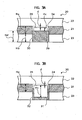
- FIG. 3A is a composition diagram when mounting an electronic component 25 in a bottomless hole 24 of the core member 21.
- the variation in FIG. 3A places a bottomless hole 29 also in the rear side resin layer 23 loaded with a height size adjustment member 30 which constitutes two bottomless holes 24, 29 from good thermally conductive material (for example, copper, etc.) and an electronic component 25 is placed and mounted on this height size adjustment member 30.
- the above-stated size differential d can be readily set to a desired value and various electronic components with different height sizes can be conveniently embedded in the composite multi-layer substrate 20.
- good thermally conductive material is used as the height size adjustment member 30, heat generated by an electronic component 25 can be dissipated from the height size adjustment member 30 to the core member 21 via the internal surface of a bottomless hole 29. Further, heat can be dissipated also to the exterior from the underside of the height size adjustment member 30 and the heat dissipation effect of an electronic component 25 can be improved much more.
- FIG. 3B is a composition diagram when mounting an electronic component 25 in a bottomless hole 24 of the core member 21.
- the variation in FIG. 3B makes it possible to apply an electronic component 25 with a large height size.
- the height size Hc of an electronic component 25 exceeds the depth size Ha of the core member 21 (Ha ⁇ Hc).
- This electronic component 25 is mounted on both sides of a bottomless hole 24 formed in the core member 21, a bottomless hole is formed in the rear side resin layer 23. A portion of the underside of an electronic component 25 and the sides are held via a thermally conductive resin 32 in two holes (a bottomless hole 24 and bottomless hole 31).
- the above-stated size differential d can be readily set as the desired value.
- Heat generated by an electronic component 25 can be dissipated from the thermally conductive resin 32 to the core member 21 via the internal surface of a bottomless hole and can also be dissipated from the underside of the thermally conductive resin 32 to the exterior.
- the heat dissipation effect of an electronic component 25 can be improved still more.
- FIGs. 4A and 4B is a main cross sectional plan view in another section of the core member 21 and an external perspective view of the section.
- a column segment 33 is set in an optional position (although adjacent to a bottomless hole 24 in the drawing, it is not limited to this) of the core member 21.
- the column segment 33 is originally a portion of the core member 21. Specifically, it is a "remaining part" of the core member 21 produced by having formed a cylindrical dividing groove 34 in an optional position of the core member 21.
- a column segment 33 can be used as follows. Namely, when a via hole 35, 36 is formed in both the front side resin layer 22 and the rear side resin layer 23 and an electrode 37, 38 is formed in the via hole 35, 36 in both directions of one end side and the other end side of the column segment 33 (island-shaped sections), the electrode 37, 38 are electrically connected via a column segment 33.
- each of the electrode 37, 38 is exposed to the front and rear surfaces of the composite multi-layer substrate 20
- the electrode 37, 38 and the column segment 33 can be used as double-sided penetration wiring of the composite multi-layer substrate 20.
- an electrical signal or power supply voltage transmission path can be obtained.
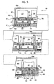
- FIG. 5 is a cross sectional plan view of a module 40 applied to the present invention.
- module (the United Kingdom: module) signifies "a standardized unit.” Although a module is interpreted as a type of unit or component, a unit is usually situated as an exchangeable integrant part. Amodule does not assume replacement parts being situated as a minimum configuration module by itself and further is designed and manufactured as an apparatus with a specific function in most cases. However, since in actuality that precise categorization is not defined, in the description it is assumed that this terminology (“module”) is defined as follows.
- a module 40 as shown in FIG. 5 can function as a power amplifier module which is an integral part of an Radio Frequency (RF; high-frequency wave) section in a portable telephone or a Personal Digital Assistant (PDA) with a wireless communications device, an antenna switch module or an RF module which unifies these and can be distributed in the marketplace by itself as a product.
- RF Radio Frequency
- PDA Personal Digital Assistant
- Amodule 40 actualizes desired circuitry (a power amplifier module, an antenna switch module or an RF module that unified these) by mounting the necessary electronic components in the front surface and inner section of a composite multi-layer substrate having a structure which applies the technical concept of the above-mentioned embodiments (first through third embodiments).
- the module 40 structure can be roughly divided into an intermediate layer A, a upper rank layer B laminated to the intermediate layer A upper surface, and a lower rank layer C laminated to the intermediate layer A lower surface.
- the intermediate layer A is laminated to a front side resin layer 42 and a rear side resin layer 43 respectively to both sides of a core member 41.
- a plurality (cross sectional plan view shows four) of bottomless holes 44 ⁇ 47 are formed in the core member 41 and has a structure embedded with suitable electronic components 48 ⁇ 51 for each of the bottomless hole 44 ⁇ 47.
- the electronic component 48 on the left end is a semiconductor chip with a short height size
- the electronic component 49 which is second from the left is a capacitor (the height size is the depth size level of the core member 41)
- the electronic component 50 which is third from the left is a resistor (the height size is the depth size level of the core member 41)
- the electronic component 51 is a semiconductor chip with a tall height size.
- the electronic component 49, 50 with a height size about the depth size of the core member 41 are embedded and mounted in the bottomless hole 45, 46 respectively.
- the electronic component 49, 50 are a capacitor and a resistor respectively. Since these components generate relatively little heat, the limitations of particular heat countermeasures are not required.
- An adhesive 52, 53 may be filled in between the rear side resin layer 43 to perform adhesion of the electronic component 49, 50. When heat generation of the component is severe, a good heat conductor should be used for the adhesive 52, 53 respectively.
- a height size adjustment member 54 is put in and the height size is adjusted.
- a good heat conductor is used for the material of the height size adjustment member 54.
- the height size is adjusted by embedding so that the rear side resin layer can be reached.
- the sides and underside of the electronic component 51 are covered and laminated with a thermally conductive resin 55.
- the height size adjustment member 54 and a thermally conductive resin 55 which borders the portion of the core member 41 and the portion of the base section exposed from the intermediate layer A underside.
- a column segment 56, 57 is set in an optional position of the core member 41. Also, the column segment 56, 57 constitute signal transmission paths or power supply transmission paths which penetrate the intermediate layer A front and rear with an electrode 58, 59, 60, 61 established so as to connect to both sides. In the intermediate layer A, 62 ⁇ 75 are electrodes.
- the lower rank layer C forms an electrode pattern (described later in detail) of the required shape in both sides of a resin layer 76 and the upper rank layer B also forms an electrode pattern (described later in detail) of the required shape in both sides of a resin layer 77. Also, surface mounting of an electronic component 78 ⁇ 82 is performed on a predetermined electrode pattern. A covering cover 40a (desirable for functioning as electromagnetic shielding for EMI measures) is attached for the electronic component 78 ⁇ 82.
- the electronic component 78, 79 and 81 is a capacitor and the electronic component 80, 82 is a resistor.
- the module 40 uses a plate-like core member 41 consisting of material (Cu (copper), Alloy 42, Invar, etc.) having excellent electrical conductivity, excellent heat conductivity and high rigidity, as well as a structure built up with the resin layers 76, 77 in the front and rear surfaces of the core member 41.
- the two resin layers 76, 77 for example, are both made with a resin, such as epoxy, polyimide, polycyanate ester, Teflon (trademark), etc. as the main ingredients (functional powder, such as dielectric powder and magnetic substance powder mixed in by desire is also good) or an insulating material used for a printed circuit board can be used.
- the characteristic is in the point of view (namely, the point of view which is a glass cloth less layer) of not having a glass cloth 7 (referring to FIG. 12 ) explained at the beginning.
- the flexural rigidity of the module 50 is obtained by the core member 41 which mainly has an intermediate layer A base, it does not require the glass cloth 7 as reinforcing material.
- the four cavities (those which form the bottomless hole 44 ⁇ 47) of the core member 41, a semiconductor chip (electronic component 48, 51), a capacitor (electronic component 49) and a resistor (electronic component 50) are each embedded. Then, among those electronic components which generate a large amount of heat (electronic component 48, 51), the bottom portion of each component and side surfaces (when required) are each connected to the core member 41 via a good thermally conductive material (height size adjustment member 54 and thermally conductive resin 55) and also connected with the upper surface electrode pattern 82, 83 of the lower rank layer C.
- the core member 41 dissipates via the internal surface of the bottomless holes. Furthermore, an electronic device substrate which mounts the module 40 will dissipate heat via the underside of an electrode pattern 86 of the lower rank layer C. Thus, sufficient heat dissipation can be acquired.
- a semiconductor chip electronic component 48
- the height size adjustment member 54 An independent member or built up with plating. It has excellent heat conductivity and the height size adjustment of the electronic component 48 is carried out.
- a cavity those which are formed in the bottomless hole 44 of the core section 41 and a through hole of the same position.
- the lower rank layer C it can be raised to a mounting height in the desired position and the relation (refer to the relation of La and Lb of FIG. 2 ) between the upper surface height position of the electronic component 48 and the upper surface height position of the core member 41 can be maintained appropriately.
- the relation (refer to the relation of La and Lb of FIG. 2 ) between the upper surface height position of the electronic component 51 and the upper surface height position of the core member 41 can be maintained appropriately by placing an electronic component into a cavity (those which are formed in the bottomless hole 47 of the core part 41 and a through hole of the same position) formed in the lower rank layer C.
- Patterning formation of the bottomless hole 44 ⁇ 47 or the column segment 56, 57
- the intermediate layer A of the core member 41 should be performed in the state where the rear side resin layer 43 emulates the underside of the core member 41. Because of the "island" shaped sections which are not removed in particular, the sections can be used as the column segment 56, 57 when the core member 41 is patterned in this state. Therefore, a columnar structure (what is called a "mailbox”: those which are formed of the electrode 58, 59, 60 and 61 connected with the column segment 56, 57 to both ends) for connecting the front and rear of the intermediate layer A can be readily formed by physical processing (for example, etching) of the core member 41.
- the core member 41 material can be made from Cu (copper), Alloy 42, Invar, etc. from a relation of physical properties.
- a common etchant such as Ferric Chloride, etc.
- the core member 41 material can be made from Cu (copper), Alloy 42, Invar, etc. from a relation of physical properties.
- Alloy 42 and Invar it is preferred to perform Cu plating to the front surface of Alloy 42 or Invar from the prevention standpoint of ion migration, etc.
- a plate-like core member 41 having excellent electrical conductivity, excellent heat conductivity and high rigidity comprising, a laminated resin layer (rear side resin layer 43) on the underside (referring to the upper and lower side directions in the drawing) of core member 41, for example, Cu, Alloy 42 or Invar, etc. and further, a thin film 90 having excellent electrical conductivity, excellent heat conductivity and high rigidity on the underside of the rear side resin layer 43 is glued together.
- an insulating material for example, such as epoxy, polyimide, cyanate ester, Teflon (registered trademark), etc. used for a resin material or printed circuit boards can be used.
- an insulating material for example, such as epoxy, polyimide, cyanate ester, Teflon (registered trademark), etc. used for a resin material or printed circuit boards can be used.
- the thin film 90 having the above-mentioned characteristics typically copper foil can be used.
- solutions which unify the rear side resin layer 43 and the thin film 90 may be used.
- an apparatus which uses copper foil with resin or copper foil glued together to dry film can be used.
- the core member 41 is patterned and the bottomless hole 44 ⁇ 47 and the column segment 56, 57 are formed.
- the bottomless hole 44 ⁇ 47 each constitute a cavity for embedding the electronic component 48 ⁇ 51.
- Patterning of the core member 41 can be carried out, for example, by applying a subtractive process.
- an etchant current used with ordinary printed circuit boards such as Ferric Chloride or Cupric Chloride (acid based) etchant, etc. can be used.
- the rear side resin layer 43 underneath is removed in the same opening shape as the bottomless hole 44, 47 (refer to the dotted line section) and the thin film 90 is exposed. Removal of the rear side resin layer 43, for example, canbe carried out, for example, by laser abrasion, plasma etching, etc.
- FIGs. 7 shows outline views after the third process in which FIG. 7A illustrates the upper surface side perspective view and FIG. 7B is the lower surface side perspective view. Also, FIG. 7 and the above-stated process diagrams ( FIG. 6A ⁇ 6C ) do not strictly correspond.
- the points of view that shouldbe understood in FIG. 7 are the "cavities" and the "mailbox" which are formed in the core member 41. Accordingly, as shown in FIGs. 7A and 7B , the resin layer 91 (equivalent to the rear side resin layer 43 of FIG. 6 ) and copper foil 92 (equivalent to the thin film 90 of FIG. 6 ) are glued together on the underside of the core member 41.
- the core member 41 is patterned with several of the cavity 93 ⁇ 95 (equivalent to the bottomless hole 44 ⁇ 47 in FIG. 6 ) and several mailbox 96 ⁇ 103 (equivalent to the column segment 56, 57 in FIG. 6 ) are formed.
- the height size adjustment member 54 is inserted into the bottomless hole 44 on the left end and thermally conductive resin 104 is applied to the height size adjustment member 54.
- the adhesive 52, 53 is applied to the second and third of the bottomless hole 45, 46 from the left and further the thermally conductive resin 55 is applied to the right end bottomless hole 47.
- the height size adjustment member 54 may be independent (stand-alone) or may be built up with plating, such as Cu, etc. It only has to have excellent heat conductivity and be able to perform height size adjustment of the electronic component 48.
- the thermally conductive resin 104, 55 has a function which performs temporary fastening of the embedded electronic component 48, 51 while also having a heat dissipation effect.
- the adhesive 52, 53 only need to have a function which mainly fixes (bonds) the embedded electronic component 49, 50.
- the embodiment is not limited to this.
- the first process FIG. 6A
- lamination is completed wherein non-hardened sections remain without performing a full cure of the resin layer when the core member 41 and the resin layer (rear side resin layer 43) are glued and laminated.
- the electronic component 49, 50 mounted in the fourth process FIG. 8A
- the adhesive 52, 53 coating operation can be considered unnecessary.
- the electronic component 48 ⁇ 51 respectively corresponding to each of the bottomless hole 44 ⁇ 47 are mounted.
- heat can be dissipated to the core member 41 and the thin film 90 via the thermally conductive resin 104 and the height size adjustment member 54.
- heat can be dissipated to the core member 41 and the thin film 90 via the thermally conductive resin 55.
- the coremember 41 is encapsulated by a resin.
- the front side resin layer 42 in the first through third embodiments is formed and the crevices surrounding the front surface of the core member 41, cavities (bottomless hole 44 ⁇ 47) and through mailboxes (column segment 56, 57) are completely covered by the front side resin layer 42.
- the side resin layer may be set in another body with the front side resin layer.
- an insulating material for example, a resin material, such as an epoxy, polyimide, cyanate ester, Teflon (registered trademark), etc. for printed circuit boards can be used.
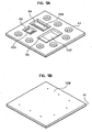
- FIGs. 9A and 9B are outline views after the fifth process and after the sixth process respectively. Also, FIG. 9 and the above-stated process diagrams ( FIG. 8A ⁇ 8C ) do not strictly correspond.
- the point of view that should be understood in FIG. 9 is the mounted state of the electronic components to a "cavities" formed in the core member 41 and the sealed state by means of a resin (front side resin layer 42). Accordingly, as shown in FIG. 9 , the electronic component 105 ⁇ 107 (equivalent to the electronic component 48 ⁇ 51 of FIG. 8 ) are mounted correspondingly in each of the cavity 93 ⁇ 95 formed in the core member 41.
- the core member 41 in the state whereby the electronic components 105 ⁇ 107 are mounted is completely encapsulated by a resin 108 (equivalent to the front side resin layer 42 of FIG. 8 ).
- a resin 108 equivalent to the front side resin layer 42 of FIG. 8 .
- FIG. 9B for convenience of the diagram, the sides of the core member 41 after encapsulating by a resin 108 are exposed. The sides are also actually covered completely by the resin 108.
- the thin film 90 is patterned.
- the heat dissipation pattern 83 for dissipating direct heat to the thin film 90 via thermally conductive resin 55 among the electronic component 48, 51 which require heat dissipation countermeasures is formed. That is, etching of the thin film 90 is performed so that the heat dissipation pattern 83 remains.
- the groove 109 ⁇ 125 are made in each of the front side resin layer 42 and the rear side resin layer 43.
- a groove 109 ⁇ 125 is formed by removing the residual substance of the resin by permanganic acid, plasma ashing, etc.
- the resin front surface may be roughened by permanganic acid, etc. and enhancement processing of the surface areas may be performed.
- 126 ⁇ 154 are an electrode or a circuit pattern which are formed in each exposed surface of the front side resin layer 42 and the rear side resin layer 43.
- the intermediate layer A in FIG. 5 is produced by this tenth process.
- the upper rank layer B and the lower rank layer C in FIG. 5 are formed by lamination in resin of each of the front side resin layer 42 and the rear side resin layer 43 and by forming a necessary solder resist pattern for the front and rear of those resin.
- FIGs. 11A and 11B are outline views after the tenth process which illustrates an upper surface side perspective view and an underside perspective view respectively.
- the point of view that should be understood in FIG. 11 is the upper rank layer B is laminated on the intermediate layer A and the lower rank layer C is laminated under the intermediate layer A.
- the necessary electric conductivity pattern 155 ⁇ 170 formed in the exposed surface of the upper rank layer B and the lower rank layer C should be understood. Those which are positioned in the exposed surface of the lower rank layer C among the electric conductivity pattern 155 ⁇ 170 and has the greatest area (electric conductivity pattern 166) is used as a heat dissipation pattern for dissipating the heat of the electronic component 48 and 51.
- the module 50 shown in FIG. 5 is completed by attaching necessary surface mount components (electronic component 78 ⁇ 82 of FIG. 5 ) after performing the above processes and attaching a cover 40a when needed.
- the module 40 which has such a structure has the following results.
- the present invention comprises a core member having sufficient rigidity to resolve and eliminate various inconveniences (Namely, aggravation of electrical properties by accompanying generation of ion migration and the increased manufacturing cost accompanying the glass cloth cutting process) that accompany the use of conventional art type glass cloth as a reinforcing fabric material.
- the present invention comprises a core member having sufficient rigidity to resolve and eliminate various inconveniences (Namely, aggravation of electrical properties by accompanying generation of ion migration and the increased manufacturing cost accompanying the glass cloth cutting process.) that accompany the use of conventional art type glass cloth as a reinforcing fabric material.
- the core member uses a metallic core material the desired rigidity can be ensured and thus making the glass cloth fabric no longer necessary, and further the core member can be used also as an electrical signal path and as a heat dissipation path.
- the core member is entirely covered by resin material and the core member is isolated from ambient air.
- deterioration by oxidization, etc. can be prevented and durability can be improved.
- using other sections of the core member and divided column segments can be used as a part of the electrical signal transmission path or power supply voltage transmission path to the direction of the front and rear surfaces of the substrate and flexibility of the wiring design can be improved.
- the core member can be used as a heat dissipation path of electronic components, and especially in cases when embedding electronic components which generate a large amount of heat can be considered as a suitable object.
- the upper surface height position of electronic components can respond to loading at the time of manufacturing the composite multi-layer substrate and breakage of the electronic components can be prevented.
- the height relation between electronic components and the core member can be adjusted and the upper surface height position of the core member can be made higher than the upper surface height position of an electronic component.
- the height size adjustment member used for the height size adjustment can be used also as a heat dissipation member.
Landscapes
- Engineering & Computer Science (AREA)
- Microelectronics & Electronic Packaging (AREA)
- Production Of Multi-Layered Print Wiring Board (AREA)
- Cooling Or The Like Of Electrical Apparatus (AREA)
- Cooling Or The Like Of Semiconductors Or Solid State Devices (AREA)
- Structure Of Printed Boards (AREA)
Description
- This invention relates to a composite multi-layer substrate andmoduleusinga substrate designedtomake high density mounting of electronic components feasible.
- Conventionally, package miniaturization has been vigorously carried out as the approach for high density mounting of electronic components. For example, recently the Chip Size Package (CSP) and ultimately bare chip mounting which makes the package itself redundant have been realized. However, each of these is premised on arranging and mounting (flat surface mounting method) a plurality of electronic components in a two-dimensional (surface) array. By simple calculation, the fundamental limitation of not being able to reduce the mounting surface areas to less than the size of the added area of each electronic component is retained.
- Therefore, a mounting method using embedded mounting of the electronic components in a substrate (more specifically, not only the substrate face) but also the inner section of the substrate attracts attention.
- Hereafter, widely known technologies of embedded mounting and their associated drawbacks will be explained.
- As an electronic component embedded structure using an organic system substrate, the electronic components are mounted in the front surface of the organic substrate serving as the core (hereinafter "core substrate"). In the case of multi-layering, a structure which encapsulates electronic components in a dielectric (nonconductive) prepreg resin is known (hereinafter "first prior art example"). Furthermore, a structure in which grooves are formed in an organic system substrate wherein electronic components are embedded is known (hereinafter "second prior art example").
- Furthermore, as for mounting electronic components on the front surface of a core substrate, a structure (hereinafter "third prior art example") in which holes corresponding to the size of electronic components are drilled in the prepreg and the electronic components are inserted and embedded in the holes of the prepreg when multi-layering or a structure (hereinafter "fourth prior art example") with embedded sintered components by transfer in organic resin are known.
- However, the first prior art example and the fourth prior art example have a drawback of being disadvantageous to thin-sizing the substrate. Also, in the second prior art example and the third prior art example, there is a drawback mentioned which involves the processing cost of the grooves or holes. Moreover, because electronic component heat dissipation countermeasures are not entirely taken into consideration, any of the prior art examples (first through fourth prior art examples) have a drawback causing inconvenience in mounting electronic components especially in regard to heat generation in larger semiconductor chips, etc.
- Japanese Laid-Open Patent Application (Kokai) (A) No.
S54-008871 (1979 - Japanese Laid-Open Patent Application (Kokai) (A) No.
S61-287194 (1986 - Japanese Laid-Open Patent Application (Kokai) (A) No.
S64-011400 (1989 - Japanese Laid-Open Patent Application (Kokai) (A) No.
S64-012598 (1989 - Japanese Laid-Open Patent Application (Kokai) (A) No.
H02-122534 (1990 - Japanese Laid-Open Patent Application (Kokai) (A) No.
2002-111226 -
FIG. 12A is a cross sectional plan view of the composite multi-layer substrate described in the official gazette. This compositemulti-layer substrate 1 has a stacked multi-layer structure of a plurality of layers. The illustrated example has four layers (described later "resin layers") 2~5 which are composed of resin material. Theseresin layers 2~5 are common in that all use resin materials, such as epoxy, etc., for the material (so-called glass cloth 7) and only the layer of the resin layer 2 (drawing top layer) is different in the respect that aglass fiber 6 is contained within the braided (knitted) shape of a net as shown inFIG. 12B . Theglass cloth 7 is reinforcement for enhancing the physical strength of the compositemulti-layer substrate 1. For convenience of explanation hereinafter, while theresin layer 2 which "has" theglass cloth 7 is denoted as "glass cloth layer 2," theresin layers 3~5 which "do not have" theglass cloth 7 are denoted as "glass clothless layers 3-5." - Further, this composite
multi-layer substrate 1 is bonded to copper foil on the bottommost surface (underside of the glass clothless layer 5) as the mounting side. The conductor pattern of copper foil is created by etching techniques, and the conductor pattern 8 of the required shape is formed. Also, some of theglass cloth layer 2 is eliminated wherein a concavity 9 (It is called a mold cavity whereas an opening is generally closed.) is formed and the electronic components 10 (for example, semiconductor chips) are mounted in theconcavity 9. - The
electronic components 10 "are embedded" by using the inner section of the compositemulti-layer substrate 1. Accordingly, other components can be mounted to the compositemulti-layer substrate 1 front surface along with components mounted in higher density. - However, since the invention described in the above-mentioned official gazette (tenth prior art example) uses the
glass cloth 7 as reinforcement for enhancing the physical strength of the composite multi-layer substrate 1: - (1) There is a problem of ion migration occurring relative to the interface of the
glass fiber 6 and the resin (the main material of the glass cloth layer 2), whereby the insulation becomes destroyed depending on the intensity of the electrolysis and resultant deterioration in the electrical properties. - (2) In order to form the
concavity 9 for the mold cavity, it is necessary to physically remove some of theresin layer 2. In that case, theglass fiber 6 within theresin layer 2 must be severed. Although such a cutting operation commonly uses precision processing machines, such as laser, etc., truncation errors are undeniable and considerable production time is also required. Moreover, when a plurality of theconcavity 9 is required, there is a problem that the production time proportionately increases which incurs higher manufacturing costs. -
JP 2001 298273 A JP 06 140461 A - Therefore, the present invention's purpose is to prevent deterioration of the electrical characteristic accompanying the generation of migration and aiming at reduction of the manufacturing cost by using other reinforcement as a substitute for the glass cloth.
- The invention is defined in
claim - Various embodiments are defined in the dependent claims.
- The present invention has been made in view of the conventional prior art drawbacks mentioned above. The present invention is constituted with a composite multi-layer substrate comprising a flat plate-like core member formed of a material having excellent electric conductivity, excellent heat conductivity and high rigidity; a front side resin layer and a rear side resin layer covering at least a front surface and a rear surface of the core member; and a bottomless hole formed in the core member penetrates the front and rear of the core member, wherein an electronic component is mounted in the bottomless hole.
- Further, the present invention is constituted with a composite multi-layer substrate comprising a flat plate-like core member formed of a material having excellent electrical conductivity, excellent heat conductivity and high rigidity; a front side resin layer and a rear side resin layer covering
- at least a front surface and a rear surface of the core member; and a flat bottomed hole formed in the core member opening in either the front surface side or rear surface side of the core member wherein an electronic component is mounted in the flat bottomed hole.
- Here, the present invention is not limited in particular. What is essential is just to have a combination of the three above-stated properties: "material which has excellent electrical conductivity, excellent heat conductivity and high rigidity."
- According to the present invention, as the core member consists of"materialwhich has excellent electrical conductivity, excellent heat conductivity and high rigidity," typically, a core member made from metal (metallic) is preferred, but copper,
Alloy 42, Invar, etc. are particularly preferred. - Additionally, though each "bottomless hole" and "bottomed hole" are used to mount an electronic component (an electronic component is a general term of a passive component part, such as a semiconductor chip, a transistor, a resistance element, a capacitative element, an inductance element or other electronic components), the first is different in terms of a "a hole without a bottom (or a through hole) " and the latter "a hole with a bottom (or a concave portion)". Also, the opening shape of a "bottomless hole" and a "bottomed hole" should just have an appropriate shape (for example, a little higher shape than the outside of the electronic component) which can conveniently mount a target electronic component.
- In a composite multi-layer substrate which has these characteristics, in order to have a core member which has rigidity, it is not necessary to use glass cloth as a reinforcing material. Therefore, various kinds of inconveniences (namely, aggravation of electrical properties by an accompanying generation of ion migration and the increased manufacturing cost accompanying the glass cloth cutting process) which accompany glass cloth are avoided.
- According to the present invention, the composite multi-layer substrate further comprises a side surface resin material which covers the side surfaces of the core member; and the core member is entirely covered by the side surface resin material, the front side resin layer and the rear side resin layer.
- According to the present invention, the composite multi-layer substrate comprises a column segment which divides the structure of the core member and penetrates the front and rear surfaces in the thickness direction of the core member; and the column segment is used as part of the electrical signal transmission path or power supply voltage transmission path to the direction of the front and rear surfaces of the substrate.
- According to the present invention in the composite multi-layer substrate, the core member is used as a heat dissipation path of an electronic component through the inner wall of the bottomless hole or the flat bottomed hole when an electronic component is mounted in the bottomless hole or the flat bottomed hole.
- According to the present invention, the composite multi-layer substrate wherein the upper surface height position of an electronic component after mounting in the bottomless hole or the bottomed hole, at least, does not cross the upper surface height position of the core member.
- According to the present invention, the composite multi-layer substrate wherein a height size adjustment member is interposed between the bottom of an electronic component when an electronic component height size is lower than the depth size of the core member mounted in the bottomless hole; and the height size adjustment member performs mounting height adjustment of an electronic component.
- According to the present invention, the composite multi-layer substrate wherein the height size adjustment member constitutes material which has heat conductivity.
- According to the present invention, a module is constituted using the composite multi-layer substrate.
- The above and further objects and novel features of the present invention will more fully appear from the following detailed description when the same is read in conjunction with the accompanying drawings. It is to be expressly understood, however, that the drawings are for the purpose of illustration only and are not intended as a definition of the limits of the invention.
-
-
FIGs. 1A~1C are main cross sectional plan views and a main perspective view of a composite multi-layer substrate in the embodiment; -
FIGs. 2A and 2B are composition diagrams when mounting anelectronic component 25 in abottomless hole 24 of thecore member 21; -
FIGs. 3A and 3B are composition diagrams when mounting anelectronic component 25 in abottomless hole 24 of thecore member 21; -
FIGs . 4A and 4B is a main cross sectional plan view in another section of thecore member 21 and an external perspective view of the section; -
FIG. 5 is a cross sectional plan view of amodule 40 applied to the present invention; -
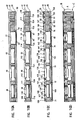
FIGs. 6A~6C are manufacturing process diagrams (first through third processes) of amodule 40; -
FIGs. 7A and 7B are outline views after the third process; -
FIGs. 8A~8C are manufacturing process diagrams (fourth through sixth process) of amodule 40; -
FIGs. 9A and 9B are outline views after the fifth and sixth processes; -
FIGs. 10A~10D are manufacturing process diagrams (seventh through tenth processes) of amodule 40; -
FIGs. 11A and 11B are outline views after the tenth process; and -
FIGs. 12A and 12B show a cross sectional plan view of a conventional prior art composite multi-layer substrate and an enlarged plan view of the glass cloth. - Hereinafter, the embodiments of the present invention will be explained with reference to the drawings.
-
FIGs. 1A-1C are main cross sectional plan views and a main perspective view of a composite multi-layer substrate in the form of the embodiment. In this cross sectional view, the compositemulti-layer substrate 20 has a "multi-layer structure. " Referring to the example illustration, the compositemulti-layer substrate 20 has a three-layer structure comprising acore member 21, a resin layer 22 (hereinafter "substrate front side resin layer") and a resin layer 23 (hereinafter "substrate rear side resin layer. " Thecore member 21 in the shape of a flat plate-like board is composed of a material which has excellent electrical conductivity, excellent heat conductivity and high rigidity. The substrate frontside resin layer 22 covers the front surface of the core member 21 (in the direction of the drawing, the upper surface). The substrate rearside resin layer 23 covers the rear surface of the core member 21 (in the direction of the drawing, the lower surface). - The essential physical characteristics for the
core member 21 are the above-mentioned three: excellent electrical conductivity, excellent heat conductivity and high rigidity. "Excellent electrical conductivity" pertains to the property of a material that allows electricity to pass through easily (that is, electrical resistance is low). "Excellent thermal conductivity" pertains to the ability to convey heat easily (that is, thermal conductivity is high). "High rigidity" pertains to minimal stress deformations due to bending or compressing. The construction material is not limited. What is essential is just to have the above-mentioned physical characteristics. Typically, metal (metallic) is preferred and especially more preferable when metals such as Cu (copper),Alloy 42, Invar, etc., are used which simultaneously satisfy the above-mentioned three physical characteristics. - Additionally, the material of the resin layers (the substrate front
side resin layer 22 and the substrate rear side resin layer 23) covering the front and rear of thecore member 21 has electrical insulating and environmental capabilities (water resistant, acid resistant, etc.), and if required further has the necessary dielectric constant. An insulating material, for example, such as epoxy, polyimide, cyanate ester, Teflon (registered trademark), etc., used for a resin material or printed circuit boards can be used. - A through hole 24 (hereinafter "bottomless hole") of predetermined opening shape is formed in the
core member 21 and penetrates the front and rear (refer toFIGs. 1A and 1B ). Thebottomless hole 24 is used as a mounting hole of anelectronic component 25. Hence, anelectronic component 25 is mounted (embedded) in the inner part of the compositemulti-layer substrate 20 and improvement of high density packaging can be achieved. - According to the composite
multi-layer substrate 20 which has such a structure, physical strength (flexural rigidity, etc.) of the compositemulti-layer substrate 20 can be acquired with the rigidity of thecore member 21. Therefore, the reinforcing material (glass cloth 7; refer toFIG. 12 ) used in the past can be made redundant and various inconveniences related to the application of the glass cloth can be avoided. - Namely, as the
core member 21 which has "high rigidity" at least uses other reinforcement material which replaces the glass cloth, the problem of ion migration explained earlier [Ion migration occurs relative to the interface of theglass fiber 6 front surface and the resin, whereby the insulation becomes destroyed and the electrical characteristic is deteriorated.]; and the problem of increased manufacturing cost [In order to form a bottomedhole 9 for a cavity, it is necessary to physically remove a portion of theresin layer 2. In that case, even though the innerpart glass fiber 6 ofresin layer 2 must be severed and such a cutting operation uses a precision processing apparatus, for example generally a laser, etc., a truncation error cannot be denied and considerable work hours are required. Moreover, when a plurality of the bottomedhole 9 is necessary, the number of needed work hours only redoubles which causes a rise in manufacturing cost. ] can be solved. Thus, the ultimate objects of the present invention (to avoid deterioration of the electrical characteristic accompanying generation of migration and to cutback the manufacturing cost) can be achieved. - In addition, although the above explanation showed an example of mounting an
electronic component 25 in thebottomless hole 24 formed in thecore member 21, an electronic component mounting hole does not necessarily have to be a hole (namely, a bottomless hole) which "penetrates front and rear." For example, as shown inFIG. 1C , a concave portion 26 (hereinafter "flat bottomed hole") may be formed in thecore member 21 and anelectronic component 25 can be mounted in a bottomedhole 26. In this manner, by direct contact or via heat conductive adhesive, etc. between anelectronic component 25 and the base of a flat bottomedhole 26, etc., the heat generated by anelectronic component 25 can efficiently escape to thecore member 21. Thus, thecore member 21 can be used for heat dissipation of anelectronic component 25. - Also, it isdesirable to presume that the resin layer structure (selection, thickness, etc.) for the front and rear surface sides of the
core member 21 be approximately the same. The compositemulti-layer substrate 20 front and rear surfaces are made into a symmetrical structure. Because the resin layers on the front and rear surface sides (frontside resin layer 22 and rear side resin layer 23) of thecore member 21 lessen differential thermal expansion, "curvature" of the compositemulti-layer substrate 20 can be controlled. - As stated above, even though the front and rear surface sides of the
core member 21 are each covered by the frontside resin layer 22 and the rearside resin layer 23, it is desirable when the sides of thecore member 21 are also covered by resin, etc. That is, it is desirable to completely enclose (sealant or coating) "all the surfaces" of thecore member 21 with an environmentally resistant material equivalent to resin or thereto. Since the front and rear surfaces of thecore member 21 each covered by the frontside resin layer 22 and the rearside resin layer 23 are not unprotected to ambient air, there is no concern about oxidation. However, when the sides of thecore member 21 are exposed, there is a possibility that the surfaces may oxidize gradually and generate an electrical short circuit, etc. causing a malfunction between the mounted components adjoining this exposure. -
FIGs. 2A and 2B are composition diagrams when mounting anelectronic component 25 in abottomless hole 24 of thecore member 21. Referring toFIG. 2A , when the upper surface height position of thecore member 21 is assumed to be La and the upper surface height position of anelectronic component 25 is assumed to be Lb, as for the differential d (d = La - Lb) of the height, it is desirable to formulate a value of zero or more than zero (namely, La = Lb or any relation of La > Lb). In this manner, since the upper surface height position La of thecore member 21 constitutes a position always higher than the upper surface height position Lb of anelectronic component 25, it can respond to the loading (load added when the frontside resin layer 22, etc. is laminated) to anelectronic component 25 on thecore member 21 at the time of manufacturing the compositemulti-layer substrate 20 and damage to anelectronic component 25 is avoidable. -
FIG. 2B is a composition diagram when mounting theelectronic component 25 in abottomless hole 24 of thecore member 21. The variation inFIG. 2B places a thermallyconductive resin 28 interposed between anelectronic component 25 and therear side layer 23 which are in contact with a side edge of the thermally conductive resin to the internal surface of abottomless hole 24 of thecore member 21. In this manner, the heat generated by anelectronic component 25 can be dissipated efficiently to thecore member 21 from the internal surface of abottomless hole 24 via the thermallyconductive resin 28. - Furthermore,
FIG. 3A is a composition diagram when mounting anelectronic component 25 in abottomless hole 24 of thecore member 21. The variation inFIG. 3A places abottomless hole 29 also in the rearside resin layer 23 loaded with a heightsize adjustment member 30 which constitutes twobottomless holes electronic component 25 is placed and mounted on this heightsize adjustment member 30. - Here, when calculating the depth size Ha of the
core member 21, the height size Hb of theresin side layer 23 and the height size Hc of the heightsize adjustment member 30, in order to adjust the differential d of the height of the upper surface position La of thecore member 21 and the upper surface height position Lb of anelectronic component 25 to the desired value, it only has to satisfy the relation of:

size adjustment member 30 is suitable as:
- Based on this, even if it is a case that the height size Hc of an
electronic component 25 is extremely small as compared with the depth size Ha of thecore member 21, the above-stated size differential d can be readily set to a desired value and various electronic components with different height sizes can be conveniently embedded in the compositemulti-layer substrate 20. Also, if good thermally conductive material is used as the heightsize adjustment member 30, heat generated by anelectronic component 25 can be dissipated from the heightsize adjustment member 30 to thecore member 21 via the internal surface of abottomless hole 29. Further, heat can be dissipated also to the exterior from the underside of the heightsize adjustment member 30 and the heat dissipation effect of anelectronic component 25 can be improved much more. -
FIG. 3B is a composition diagram when mounting anelectronic component 25 in abottomless hole 24 of thecore member 21. The variation inFIG. 3B makes it possible to apply anelectronic component 25 with a large height size. Referring toFIG. 3B , the height size Hc of anelectronic component 25 exceeds the depth size Ha of the core member 21 (Ha < Hc). Thiselectronic component 25 is mounted on both sides of abottomless hole 24 formed in thecore member 21, a bottomless hole is formed in the rearside resin layer 23. A portion of the underside of anelectronic component 25 and the sides are held via a thermallyconductive resin 32 in two holes (abottomless hole 24 and bottomless hole 31). - In this manner, even if an
electronic component 25 has a large height size, the above-stated size differential d can be readily set as the desired value. Heat generated by anelectronic component 25 can be dissipated from the thermallyconductive resin 32 to thecore member 21 via the internal surface of a bottomless hole and can also be dissipated from the underside of the thermallyconductive resin 32 to the exterior. Thus, the heat dissipation effect of anelectronic component 25 can be improved still more. -
FIGs. 4A and 4B is a main cross sectional plan view in another section of thecore member 21 and an external perspective view of the section. Referring to these drawings, acolumn segment 33 is set in an optional position (although adjacent to abottomless hole 24 in the drawing, it is not limited to this) of thecore member 21. - The
column segment 33 is originally a portion of thecore member 21. Specifically, it is a "remaining part" of thecore member 21 produced by having formed acylindrical dividing groove 34 in an optional position of thecore member 21. Acolumn segment 33 can be used as follows. Namely, when a viahole side resin layer 22 and the rearside resin layer 23 and anelectrode hole electrode column segment 33. Furthermore, because the end face of each of theelectrode multi-layer substrate 20, theelectrode column segment 33 can be used as double-sided penetration wiring of the compositemulti-layer substrate 20. Thus, an electrical signal or power supply voltage transmission path can be obtained. -
FIG. 5 is a cross sectional plan view of amodule 40 applied to the present invention. - A "module (the United Kingdom: module)" signifies "a standardized unit." Although a module is interpreted as a type of unit or component, a unit is usually situated as an exchangeable integrant part. Amodule does not assume replacement parts being situated as a minimum configuration module by itself and further is designed and manufactured as an apparatus with a specific function in most cases. However, since in actuality that precise categorization is not defined, in the description it is assumed that this terminology ("module") is defined as follows. Namely, a module which can be said to comprise one or more (a combination of electronic components of different kinds is included) electronic components (these are named generically and called an "electronic component") of a semiconductor chip, a resistance element, a capacitative element or others are mounted in the inner sections and a necessary electronic circuit function is actualized, as well as an apparatus which can be distributed individually in the marketplace. Subsequent replacement simplicity including (installing) optional electronic devices is not especially considered. It may have a mounting configuration which can be attached and detached by a connector, etc. and may be formedmountedmostly in a fixed state by soldering, etc.
- A
module 40 as shown inFIG. 5 , for example, can function as a power amplifier module which is an integral part of an Radio Frequency (RF; high-frequency wave) section in a portable telephone or a Personal Digital Assistant (PDA) with a wireless communications device, an antenna switch module or an RF module which unifies these and can be distributed in the marketplace by itself as a product. -
Amodule 40 actualizes desired circuitry (a power amplifier module, an antenna switch module or an RF module that unified these) by mounting the necessary electronic components in the front surface and inner section of a composite multi-layer substrate having a structure which applies the technical concept of the above-mentioned embodiments (first through third embodiments). - As shown in
FIG. 5 , themodule 40 structure can be roughly divided into an intermediate layer A, a upper rank layer B laminated to the intermediate layer A upper surface, and a lower rank layer C laminated to the intermediate layer A lower surface. - The intermediate layer A is laminated to a front
side resin layer 42 and a rearside resin layer 43 respectively to both sides of acore member 41. A plurality (cross sectional plan view shows four) ofbottomless holes 44~47 are formed in thecore member 41 and has a structure embedded with suitableelectronic components 48~51 for each of thebottomless hole 44~47. - Next, as an explanation for convenience, assume the
electronic component 48 on the left end is a semiconductor chip with a short height size, theelectronic component 49 which is second from the left is a capacitor (the height size is the depth size level of the core member 41), theelectronic component 50 which is third from the left is a resistor (the height size is the depth size level of the core member 41) and theelectronic component 51 is a semiconductor chip with a tall height size. - The
electronic component core member 41 are embedded and mounted in thebottomless hole electronic component side resin layer 43 to perform adhesion of theelectronic component - Moreover, if it is the
electronic component 48 with a short height size, a heightsize adjustment member 54 is put in and the height size is adjusted. When heat generation of theelectronic component 48 is severe, a good heat conductor is used for the material of the heightsize adjustment member 54. Further, if it is theelectronic component 51 with a tall height size, the height size is adjusted by embedding so that the rear side resin layer can be reached. When heat generation of the electronic component is severe, the sides and underside of theelectronic component 51 are covered and laminated with a thermallyconductive resin 55. In any case, the heightsize adjustment member 54 and a thermallyconductive resin 55 which borders the portion of thecore member 41 and the portion of the base section exposed from the intermediate layer A underside. - Besides, a
column segment core member 41. Also, thecolumn segment electrode - The lower rank layer C forms an electrode pattern (described later in detail) of the required shape in both sides of a
resin layer 76 and the upper rank layer B also forms an electrode pattern (described later in detail) of the required shape in both sides of aresin layer 77. Also, surface mounting of anelectronic component 78∼82 is performed on a predetermined electrode pattern. Acovering cover 40a (desirable for functioning as electromagnetic shielding for EMI measures) is attached for theelectronic component 78~82. Although not limited in particular, theelectronic component electronic component - Thus, the
module 40 uses a plate-like core member 41 consisting of material (Cu (copper),Alloy 42, Invar, etc.) having excellent electrical conductivity, excellent heat conductivity and high rigidity, as well as a structure built up with the resin layers 76, 77 in the front and rear surfaces of thecore member 41. Here, the tworesin layers FIG. 12 ) explained at the beginning. As the flexural rigidity of themodule 50 is obtained by thecore member 41 which mainly has an intermediate layer A base, it does not require theglass cloth 7 as reinforcing material. - The four cavities (those which form the
bottomless hole 44~47) of thecore member 41, a semiconductor chip (electronic component 48, 51), a capacitor (electronic component 49) and a resistor (electronic component 50) are each embedded. Then, among those electronic components which generate a large amount of heat (electronic component 48, 51), the bottom portion of each component and side surfaces (when required) are each connected to thecore member 41 via a good thermally conductive material (heightsize adjustment member 54 and thermally conductive resin 55) and also connected with the uppersurface electrode pattern core member 41 dissipates via the internal surface of the bottomless holes. Furthermore, an electronic device substrate which mounts themodule 40 will dissipate heat via the underside of an electrode pattern 86 of the lower rank layer C. Thus, sufficient heat dissipation can be acquired. - Additionally, as for a semiconductor chip (electronic component 48) with a short height size with the height size adjustment member 54 (An independent member or built up with plating. It has excellent heat conductivity and the height size adjustment of the
electronic component 48 is carried out.) which is placed in a cavity (Those which are formed in thebottomless hole 44 of thecore section 41 and a through hole of the same position.) formed in the lower rank layer C, it can be raised to a mounting height in the desired position and the relation (refer to the relation of La and Lb ofFIG. 2 ) between the upper surface height position of theelectronic component 48 and the upper surface height position of thecore member 41 can be maintained appropriately. - As for a semiconductor chip with a tall height size (electronic component 51), the relation (refer to the relation of La and Lb of
FIG. 2 ) between the upper surface height position of theelectronic component 51 and the upper surface height position of thecore member 41 can be maintained appropriately by placing an electronic component into a cavity (those which are formed in thebottomless hole 47 of thecore part 41 and a through hole of the same position) formed in the lower rank layer C. - Patterning (formation of the
bottomless hole 44~47 or thecolumn segment 56, 57) in the intermediate layer A of thecore member 41 should be performed in the state where the rearside resin layer 43 emulates the underside of thecore member 41. Because of the "island" shaped sections which are not removed in particular, the sections can be used as thecolumn segment core member 41 is patterned in this state. Therefore, a columnar structure (what is called a "mailbox": those which are formed of theelectrode column segment core member 41. When etching thecore member 41 with a common etchant, such as Ferric Chloride, etc., thecore member 41 material can be made from Cu (copper),Alloy 42, Invar, etc. from a relation of physical properties. However, whenAlloy 42 and Invar are selected, it is preferred to perform Cu plating to the front surface ofAlloy 42 or Invar from the prevention standpoint of ion migration, etc. - Next, the manufacturing process of the above-stated
module 40 will be explained. - A plate-
like core member 41 having excellent electrical conductivity, excellent heat conductivity and high rigidity comprising, a laminated resin layer (rear side resin layer 43) on the underside (referring to the upper and lower side directions in the drawing) ofcore member 41, for example, Cu,Alloy 42 or Invar, etc. and further, athin film 90 having excellent electrical conductivity, excellent heat conductivity and high rigidity on the underside of the rearside resin layer 43 is glued together. - Here, as the material of the rear
side resin layer 43, an insulating material, for example, such as epoxy, polyimide, cyanate ester, Teflon (registered trademark), etc. used for a resin material or printed circuit boards can be used. Also, as for thethin film 90 having the above-mentioned characteristics, typically copper foil can be used. - Basically, solutions which unify the rear
side resin layer 43 and thethin film 90 may be used. For example, an apparatus which uses copper foil with resin or copper foil glued together to dry film can be used. - Next, the
core member 41 is patterned and thebottomless hole 44~47 and thecolumn segment bottomless hole 44~47 each constitute a cavity for embedding theelectronic component 48~51. Patterning of thecore member 41 can be carried out, for example, by applying a subtractive process. In this case, an etchant current used with ordinary printed circuit boards, such as Ferric Chloride or Cupric Chloride (acid based) etchant, etc. can be used. - Next, as for the
bottomless hole electronic component 48, 51) which generate a large amount of heat, the rearside resin layer 43 underneath is removed in the same opening shape as thebottomless hole 44, 47 (refer to the dotted line section) and thethin film 90 is exposed. Removal of the rearside resin layer 43, for example, canbe carried out, for example, by laser abrasion, plasma etching, etc. -
FIGs. 7 shows outline views after the third process in whichFIG. 7A illustrates the upper surface side perspective view andFIG. 7B is the lower surface side perspective view. Also,FIG. 7 and the above-stated process diagrams (FIG. 6A~6C ) do not strictly correspond. The points of view that shouldbe understood inFIG. 7 are the "cavities" and the "mailbox" which are formed in thecore member 41. Accordingly, as shown inFIGs. 7A and 7B , the resin layer 91 (equivalent to the rearside resin layer 43 ofFIG. 6 ) and copper foil 92 (equivalent to thethin film 90 ofFIG. 6 ) are glued together on the underside of thecore member 41. Thecore member 41 is patterned with several of thecavity 93~95 (equivalent to thebottomless hole 44~47 inFIG. 6 ) andseveral mailbox 96~103 (equivalent to thecolumn segment FIG. 6 ) are formed. - Next, the height
size adjustment member 54 is inserted into thebottomless hole 44 on the left end and thermallyconductive resin 104 is applied to the heightsize adjustment member 54. Moreover, the adhesive 52, 53 is applied to the second and third of thebottomless hole conductive resin 55 is applied to the right endbottomless hole 47. The heightsize adjustment member 54 may be independent (stand-alone) or may be built up with plating, such as Cu, etc. It only has to have excellent heat conductivity and be able to perform height size adjustment of theelectronic component 48. As the name suggests, the thermallyconductive resin electronic component electronic component - Here, although the
electronic component FIG. 6A ), lamination is completed wherein non-hardened sections remain without performing a full cure of the resin layer when thecore member 41 and the resin layer (rear side resin layer 43) are glued and laminated. In the case of theelectronic component FIG. 8A ), it is possible to fix theelectronic component - Next, the
electronic component 48~51 respectively corresponding to each of thebottomless hole 44~47 are mounted. As for the firstelectronic component 48 wherein heat dissipation is necessary, heat can be dissipated to thecore member 41 and thethin film 90 via the thermallyconductive resin 104 and the heightsize adjustment member 54. Also, as for the secondelectronic component 51 wherein heat dissipation is necessary, heat can be dissipated to thecore member 41 and thethin film 90 via the thermallyconductive resin 55. - Next, after mounting the
electronic component 48∼51, thecoremember 41 is encapsulated by a resin. By means of this sealing, the frontside resin layer 42 in the first through third embodiments is formed and the crevices surrounding the front surface of thecore member 41, cavities (bottomless hole 44~47) and through mailboxes (column segment 56, 57) are completely covered by the frontside resin layer 42. Here, it is desirable to also encapsulate completely in resin the side edges (refer to the dotted line enclosure parts A and B inFIG. 8C ) of thecore member 41. As a resin which encapsulates the side edges, although it may function as a portion of the front side resin layer, the side resin layer may be set in another body with the front side resin layer. When produced in such a manner, all the surfaces of thecore member 41 are insulated from the environmental atmosphere (air) and oxidation of thecore member 41 by oxygen, moisture, etc. in the environment can be prevented. Also, electrical short circuits between adjacent mounted components, etc. is prevented and malfunctioning can be avoided. - Here, as for the material of the front
side resin layer 42, an insulating material, for example, a resin material, such as an epoxy, polyimide, cyanate ester, Teflon (registered trademark), etc. for printed circuit boards can be used. -
FIGs. 9A and 9B are outline views after the fifth process and after the sixth process respectively. Also,FIG. 9 and the above-stated process diagrams (FIG. 8A~8C ) do not strictly correspond. The point of view that should be understood inFIG. 9 is the mounted state of the electronic components to a "cavities" formed in thecore member 41 and the sealed state by means of a resin (front side resin layer 42). Accordingly, as shown inFIG. 9 , theelectronic component 105∼107 (equivalent to theelectronic component 48~51 ofFIG. 8 ) are mounted correspondingly in each of thecavity 93~95 formed in thecore member 41. Thecore member 41 in the state whereby theelectronic components 105~107 are mounted is completely encapsulated by a resin 108 (equivalent to the frontside resin layer 42 ofFIG. 8 ). InFIG. 9B , for convenience of the diagram, the sides of thecore member 41 after encapsulating by aresin 108 are exposed. The sides are also actually covered completely by theresin 108. - Next, the
thin film 90 is patterned. By this patterning, theheat dissipation pattern 83 for dissipating direct heat to thethin film 90 via thermallyconductive resin 55 among theelectronic component thin film 90 is performed so that theheat dissipation pattern 83 remains. - Next, the
groove 109∼125 are made in each of the frontside resin layer 42 and the rearside resin layer 43. For example, after partially removing each class of resin by a Carbon Dioxide (CO2) gas laser, Ultra Violet (UV) laser or excimer laser, etc., agroove 109∼125 is formed by removing the residual substance of the resin by permanganic acid, plasma ashing, etc. - Next, coppering and etching are performed to the
groove 109∼125, anelectrode 62∼75 for performing the interlayer electric connection with terminals of theelectronic component 48~49, anelectrode 58∼61 for carrying out interlayer connection through thecore member 41, etc. are formed. When necessary, in order to ensure the best adhesion of a resin and plating copper, the resin front surface may be roughened by permanganic acid, etc. and enhancement processing of the surface areas may be performed. Also, 126∼154 are an electrode or a circuit pattern which are formed in each exposed surface of the frontside resin layer 42 and the rearside resin layer 43. The intermediate layer A inFIG. 5 is produced by this tenth process. - Next, the upper rank layer B and the lower rank layer C in
FIG. 5 are formed by lamination in resin of each of the frontside resin layer 42 and the rearside resin layer 43 and by forming a necessary solder resist pattern for the front and rear of those resin. -
FIGs. 11A and 11B are outline views after the tenth process which illustrates an upper surface side perspective view and an underside perspective view respectively. The point of view that should be understood inFIG. 11 is the upper rank layer B is laminated on the intermediate layer A and the lower rank layer C is laminated under the intermediate layer A. Also, the necessaryelectric conductivity pattern 155~170 formed in the exposed surface of the upper rank layer B and the lower rank layer C should be understood. Those which are positioned in the exposed surface of the lower rank layer C among theelectric conductivity pattern 155~170 and has the greatest area (electric conductivity pattern 166) is used as a heat dissipation pattern for dissipating the heat of theelectronic component - The
module 50 shown inFIG. 5 is completed by attaching necessary surface mount components (electronic component 78~82 ofFIG. 5 ) after performing the above processes and attaching acover 40a when needed. - The
module 40 which has such a structure has the following results. - (1) Since the plate-
like core member 41 consisting of material (Cu,Alloy 42, Invar, etc.) having excellent electric conductivity, excellent heat conductivity and high rigidity is constituted as a base, bending stress of the substrate can be minimized with the rigidity of thecore member 41 and substrate deformation which is not preferred can be avoided or controlled. Therefore, since conventional reinforcement (glass cloth) in thecore member 41 is not needed, the exceptional effect of not producing associated problems related to the glass cloth (Notably, the problem of ion migration and the problem of the increased manufacturing cost accompanying the glass cloth cutting process at the time of cavity shaping.) is acquired. - (2) Since the "island" shaped sections are not removed when the column segments are formed in a needed section wherein a resin (rear side resin layer 43) is affixed on one side (embodiment rear surface) of the
core member 41, these can be used as the island-shapedsection 56, 57 (column segments). Then, the electrical signal transmission paths and power supply transmission paths between layers can easily be constituted via the island-shapedsections - (3) A cavity (
bottomless hole 44~47) can be formed in thecore member 21, as well as theelectronic components 48~51 can be readily embedded in the cavity and high density packaging of the substrate can be conjointly improved with surface mounting. - (4) When an electronic component with a short height size or tall height size is embedded, a height
size adjustment member 54 is inserted or a hole in the rear side resin layer is used. The height size of electronic components can be readily adjusted and set properly so that the upper surface height position of an electronic component does not exceed the upper surface height position of thecore member 41. For this reason, it can respond to loading at the time of manufacturing the composite multi-layer substrate and breakage of the electronic components can be prevented. - (5) When dissipating the heat of the electronic components, the
core member 41 can be used for a heat dissipation path or a heat dissipation pattern (electrode pattern 166 ofFIG. 11B ) formed in the exposed surface of the lower rank layer C can be used for heat dissipation. Especially theelectronic component module 40 constituted by embedding and can be considered as a suitable object. - (6) Curvature of the substrate can be avoided or controlled to the intermediate layer A by making the intermediate rank layer A, upper rank layer B and lower rank layer C into a substantially symmetrical structure.
- As set forth above, the advantages of the present invention will now be explained.
- The present invention comprises a core member having sufficient rigidity to resolve and eliminate various inconveniences (Namely, aggravation of electrical properties by accompanying generation of ion migration and the increased manufacturing cost accompanying the glass cloth cutting process) that accompany the use of conventional art type glass cloth as a reinforcing fabric material.
- The present invention comprises a core member having sufficient rigidity to resolve and eliminate various inconveniences (Namely, aggravation of electrical properties by accompanying generation of ion migration and the increased manufacturing cost accompanying the glass cloth cutting process.) that accompany the use of conventional art type glass cloth as a reinforcing fabric material.
- According to the present invention, since the core member uses a metallic core material the desired rigidity can be ensured and thus making the glass cloth fabric no longer necessary, and further the core member can be used also as an electrical signal path and as a heat dissipation path.
- According to the present invention, the core member is entirely covered by resin material and the core member is isolated from ambient air. Thus, deterioration by oxidization, etc. can be prevented and durability can be improved.
- According to the present invention, using other sections of the core member and divided column segments can be used as a part of the electrical signal transmission path or power supply voltage transmission path to the direction of the front and rear surfaces of the substrate and flexibility of the wiring design can be improved.
- According to the present invention, the core member can be used as a heat dissipation path of electronic components, and especially in cases when embedding electronic components which generate a large amount of heat can be considered as a suitable object.
- According to the present invention, the upper surface height position of electronic components can respond to loading at the time of manufacturing the composite multi-layer substrate and breakage of the electronic components can be prevented.
- According to the present invention, the height relation between electronic components and the core member can be adjusted and the upper surface height position of the core member can be made higher than the upper surface height position of an electronic component.
- According to the present invention, the height size adjustment member used for the height size adjustment can be used also as a heat dissipation member.
- According to the present invention, a module which has the effects of the present invention according to the claims can be produced.
- While the present invention has been described with reference to the preferred embodiments, it is intended that the invention be not limited by any of the details of the description therein but includes all the embodiments which fall within the scope of the appended claims.
Claims (5)
- A composite multi-layer substrate (20) comprising:a flat plate-like core member (21, 41) formed of a material having electric conductivity, heat conductivity and rigidity;a front side resin layer (22, 42) covering a front surface of said core member(21, 41);a rear side resin layer (23, 43) covering a rear surface of said core member (2141);a bottomless hole (24, 44) formed in said core member (21, 41) penetrating said front and rear of said core member (21, 41), andan electronic component (25, 48) mounted in said bottomless hole (24, 44), the thickness (Hc) of the electronic component (25, 48) after mounting in said bottomless hole (24, 44) is thinner than the thickness (Ha) of said core member (21, 41);
characterised in thata first groove (110, 111) which is formed in either one or both of said front side resin layer (22, 42) and said rear side resin layer (23, 43), is located directly above or directly below said electronic component (25, 48), and extends in a vertical direction of the front surface and the rear surface of said core member (21, 41);a first electrode (63, 64) is formed on an interior portion of said first groove (110, 111);a second groove (35, 36) which is formed in either one or both of said front side resin layer (22, 42) and said rear side resin layer (23, 43), is located in areas directly above or directly below said core member (21, 41) excluding areas directly above and directly below said electronic component (25, 48), and extends in the vertical direction of the front surface and the rear surface of said core member (21, 41);a second electrode (37, 38) is formed on an interior portion of said second groove (35, 36),wherein an electrical connection to said electronic component (25, 48) is provided via said first electrode (63, 64), and an electrical connection to said core member (21, 41) is provided via said second groove (35, 36), andwherein said electronic component (25, 48) is structured such that, in a state where said electronic component (25, 48) is mounted in said bottomless hole (24, 44) with reference to a position of a surface in which an opening of said bottomless hole (24, 44) is formed, a position of at least one surface facing the opening among two surfaces of said electronic component (25, 48) is embedded within an interior portion of said bottomless hole (24, 44). - A composite multi-layer substrate (20) comprising:a flat plate-like core member (21, 41) formed of a material having electrical conductivity, heat conductivity and rigidity;a resin layer (22,42;23,43) is covering a surface of said core member;a flat bottomed hole (26) formed in an opening of either one of said front surface of said core member (21, 41) or rear surface of said core member (21, 41); andan electronic component (25, 48) mounted in said flat bottomed hole (26), the thickness (Hc) of the electronic component (25, 48) after mounting in said flat bottomed hole (26) isthinner than the thickness (Ha) of said core member (21, 41);
characterised in thata front side resin layer (22, 42) is covering a front surface of said core member;a rear side resin layer (23, 43) is covering a rear surface of said core member (21, 41);a first groove (110, 111) which is formed in either one or both of said front side resin layer (22, 42) and said rear side resin layer (23, 43), is located directly above or directly below said electronic component (25, 48), and extends in a vertical direction of the front surface and the rear surface of said core member (21, 41);a first electrode (63, 64) is formed on an interior portion of said first groove (110, 111);a second groove (35, 36) which is formed in either one or both of said front side resin layer (22, 42) and said rear side resin layer (23, 43), is located in areas directly above or directly below said core member (21, 41) excluding areas directly above and directly below said electronic component (25, 48), and extends in the vertical direction of the front surface and the rear surface of said core member (21, 41);a second electrode (37, 38) is formed on an interior portion of said second groove (35, 36),wherein an electrical connection to said electronic component (25, 48) is provided via said first electrode (63, 64), and an electrical connection to said core member (21, 41) is provided via said second groove (35, 36), andwherein said electronic component (25, 48) is structured such that, in a state where said electronic component (25, 48) is mounted in said flat bottomed hole (26) with reference to a position of a surface in which an opening of said flat bottomed hole (26) is formed, a position of at least one surface facing the opening among two surface of said electronic component (25, 48) is embedded within an interior portion of said flat bottomed hole (26). - The composite multi-layer substrate (20) according to claims 1 or 2, comprises a cylindrical column segment (33) which divides said core member (21, 41) and penetrates said front and rear surfaces in the thickness direction of said core member (21, 41); and said cylindrical column segment (33) is used as part of an electrical signal transmission path or a power supply voltage transmission path to the direction of the front and rear surfaces of said substrate (20).
- The composite multi-layer substrate (20) according to claim 1, wherein said electronic component (25, 48) includes at least one electronic component (25, 48) structured such that, when said electronic component (25, 48) has an electrode on only either one of an upper surface and a lower surface of said electronic component (25, 48) and said electrode is on the upper surface, the lower surface of said electronic component (25, 48) is embedded within an interior portion of said bottomless hole (24).
- A module is constituted using said composite multi-layer substrate (20) in claims 1 through 4.
Applications Claiming Priority (3)
| Application Number | Priority Date | Filing Date | Title |
|---|---|---|---|
| JP2002156796A JP2003347741A (en) | 2002-05-30 | 2002-05-30 | Composite multilayer substrate and module using the same |
| JP2002156796 | 2002-05-30 | ||
| PCT/JP2003/006597 WO2003103355A1 (en) | 2002-05-30 | 2003-05-27 | Composite multi-layer substrate and module using the substrate |
Publications (3)
| Publication Number | Publication Date |
|---|---|
| EP1536673A1 EP1536673A1 (en) | 2005-06-01 |
| EP1536673A4 EP1536673A4 (en) | 2008-08-27 |
| EP1536673B1 true EP1536673B1 (en) | 2015-07-08 |
Family
ID=29706448
Family Applications (1)
| Application Number | Title | Priority Date | Filing Date |
|---|---|---|---|
| EP03733093.3A Expired - Lifetime EP1536673B1 (en) | 2002-05-30 | 2003-05-27 | Composite multi-layer substrate and module using the substrate |
Country Status (6)
| Country | Link |
|---|---|
| US (4) | US7348662B2 (en) |
| EP (1) | EP1536673B1 (en) |
| JP (1) | JP2003347741A (en) |
| CN (1) | CN100435604C (en) |
| AU (1) | AU2003241801A1 (en) |
| WO (1) | WO2003103355A1 (en) |
Families Citing this family (75)
| Publication number | Priority date | Publication date | Assignee | Title |
|---|---|---|---|---|
| JP4339739B2 (en) * | 2004-04-26 | 2009-10-07 | 太陽誘電株式会社 | Multi-layer board with built-in components |
| JP3914239B2 (en) * | 2005-03-15 | 2007-05-16 | 新光電気工業株式会社 | Wiring board and method for manufacturing wiring board |
| KR100726240B1 (en) | 2005-10-04 | 2007-06-11 | 삼성전기주식회사 | Electronic circuit board and manufacturing method |
| KR100704919B1 (en) * | 2005-10-14 | 2007-04-09 | 삼성전기주식회사 | Substrate without core layer and its manufacturing method |
| CN100379328C (en) * | 2005-10-20 | 2008-04-02 | 浙江大学 | Sealing frame for flat panel display device sealing and preparation method |
| KR101049389B1 (en) * | 2005-12-16 | 2011-07-14 | 이비덴 가부시키가이샤 | Multilayer printed wiring plate, and method for fabricating the same |
| KR100751995B1 (en) * | 2006-06-30 | 2007-08-28 | 삼성전기주식회사 | Printed Circuit Board and Manufacturing Method |
| KR100796522B1 (en) | 2006-09-05 | 2008-01-21 | 삼성전기주식회사 | Manufacturing Method of Electronic Circuit Board |
| KR100789530B1 (en) * | 2006-11-20 | 2007-12-28 | 삼성전기주식회사 | Chip embedded printed circuit board and its manufacturing method |
| JP4518113B2 (en) * | 2007-07-25 | 2010-08-04 | Tdk株式会社 | Electronic component built-in substrate and manufacturing method thereof |
| US8314343B2 (en) * | 2007-09-05 | 2012-11-20 | Taiyo Yuden Co., Ltd. | Multi-layer board incorporating electronic component and method for producing the same |
| JP5292847B2 (en) * | 2008-02-20 | 2013-09-18 | 住友ベークライト株式会社 | Semiconductor device mounting substrate |
| US8963016B2 (en) | 2008-10-31 | 2015-02-24 | Taiyo Yuden Co., Ltd. | Printed wiring board and method for manufacturing same |
| JP5488783B2 (en) * | 2009-01-30 | 2014-05-14 | Tdk株式会社 | Electronic component built-in substrate and manufacturing method thereof |
| KR101077410B1 (en) * | 2009-05-15 | 2011-10-26 | 삼성전기주식회사 | Printed circuit board with electronic components embedded therein including cooling member and method for fabricating the same |
| TWI405511B (en) * | 2009-07-08 | 2013-08-11 | Samsung Electro Mech | Printed circuit board with electronic components and method of manufacturing same |
| TWI501376B (en) * | 2009-10-07 | 2015-09-21 | 精材科技股份有限公司 | Chip package and method of manufacturing same |
| JP5182448B2 (en) * | 2010-02-18 | 2013-04-17 | 株式会社村田製作所 | Component built-in board |
| JPWO2011102561A1 (en) * | 2010-02-22 | 2013-06-17 | 三洋電機株式会社 | Multilayer printed wiring board and manufacturing method thereof |
| TWI530241B (en) * | 2010-03-16 | 2016-04-11 | 燿華電子股份有限公司 | A multi - layer circuit board manufacturing method for embedded electronic components |
| JP5685012B2 (en) * | 2010-06-29 | 2015-03-18 | 新光電気工業株式会社 | Manufacturing method of semiconductor package |
| KR101167453B1 (en) * | 2010-12-23 | 2012-07-26 | 삼성전기주식회사 | A printed circuit board comprising embeded electronic component within and a method for manufacturing |
| JP5370445B2 (en) | 2011-09-09 | 2013-12-18 | 株式会社村田製作所 | Power control circuit module |
| US20130258623A1 (en) * | 2012-03-29 | 2013-10-03 | Unimicron Technology Corporation | Package structure having embedded electronic element and fabrication method thereof |
| WO2014020479A2 (en) * | 2012-08-03 | 2014-02-06 | Ecole Polytechnique Federale De Lausanne (Epfl) | Post-CMOS Processing and 3D Integration Based on Dry-Film Lithography |
| JP5236826B1 (en) | 2012-08-15 | 2013-07-17 | 太陽誘電株式会社 | Electronic component built-in board |
| TW201410106A (en) * | 2012-08-24 | 2014-03-01 | Kinsus Interconnect Tech Corp | Method for build-up layers on circuit boards |
| US9293426B2 (en) | 2012-09-28 | 2016-03-22 | Intel Corporation | Land side and die side cavities to reduce package Z-height |
| KR101420526B1 (en) * | 2012-11-29 | 2014-07-17 | 삼성전기주식회사 | Substrate embedding electronic component and manufacturing mehtod thereof |
| US20140254101A1 (en) * | 2013-03-05 | 2014-09-11 | Qualcomm Incorporated | Smart phone on a chip and method making same |
| JP6105358B2 (en) * | 2013-04-02 | 2017-03-29 | 太陽誘電株式会社 | Circuit board |
| JP5888786B2 (en) * | 2013-04-02 | 2016-03-22 | 太陽誘電株式会社 | Circuit board |
| KR101497230B1 (en) * | 2013-08-20 | 2015-02-27 | 삼성전기주식회사 | Electronic component embedded substrate and method of manufacturing electronic component embedded substrate |
| KR102086792B1 (en) * | 2013-09-02 | 2020-03-09 | 삼성전자주식회사 | An electronic device including removable component |
| DE102014008148B4 (en) * | 2014-05-23 | 2020-06-04 | Continental Automotive Gmbh | Process for manufacturing a printed circuit board and printed circuit board |
| JP6742682B2 (en) | 2014-09-03 | 2020-08-19 | 太陽誘電株式会社 | Multilayer wiring board |
| JP6587796B2 (en) * | 2014-10-02 | 2019-10-09 | 太陽誘電株式会社 | Circuit module |
| US9613843B2 (en) * | 2014-10-13 | 2017-04-04 | General Electric Company | Power overlay structure having wirebonds and method of manufacturing same |
| US10433424B2 (en) * | 2014-10-16 | 2019-10-01 | Cyntec Co., Ltd | Electronic module and the fabrication method thereof |
| US9402301B2 (en) * | 2014-12-10 | 2016-07-26 | Raytheon Company | Vertical radio frequency module |
| US10109588B2 (en) | 2015-05-15 | 2018-10-23 | Samsung Electro-Mechanics Co., Ltd. | Electronic component package and package-on-package structure including the same |
| KR102021886B1 (en) * | 2015-05-15 | 2019-09-18 | 삼성전자주식회사 | Electronic component package and package on package structure |
| US9781819B2 (en) | 2015-07-31 | 2017-10-03 | Laird Technologies, Inc. | Multifunctional components for electronic devices and related methods of providing thermal management and board level shielding |
| US9852971B1 (en) * | 2016-06-09 | 2017-12-26 | Advanced Semiconductor Engineering, Inc. | Interposer, semiconductor package structure, and semiconductor process |
| JP6693441B2 (en) * | 2017-02-27 | 2020-05-13 | オムロン株式会社 | Electronic device and manufacturing method thereof |
| JP2019067858A (en) * | 2017-09-29 | 2019-04-25 | イビデン株式会社 | Printed wiring board and manufacturing method thereof |
| KR102070090B1 (en) * | 2018-03-15 | 2020-01-29 | 삼성전자주식회사 | Semiconductor package |
| US10727212B2 (en) * | 2018-03-15 | 2020-07-28 | Samsung Electronics Co., Ltd. | Semiconductor package |
| CN111341750B (en) * | 2018-12-19 | 2024-03-01 | 奥特斯奥地利科技与系统技术有限公司 | Component carrier including conductive base structure and method of manufacturing |
| US11342256B2 (en) | 2019-01-24 | 2022-05-24 | Applied Materials, Inc. | Method of fine redistribution interconnect formation for advanced packaging applications |
| US11289412B2 (en) | 2019-03-13 | 2022-03-29 | Texas Instruments Incorporated | Package substrate with partially recessed capacitor |
| US10939562B2 (en) | 2019-03-26 | 2021-03-02 | Taiyo Yuden Co., Ltd. | Multilayer board and manufacturing method of the same |
| IT201900006740A1 (en) | 2019-05-10 | 2020-11-10 | Applied Materials Inc | SUBSTRATE STRUCTURING PROCEDURES |
| IT201900006736A1 (en) | 2019-05-10 | 2020-11-10 | Applied Materials Inc | PACKAGE MANUFACTURING PROCEDURES |
| US11931855B2 (en) | 2019-06-17 | 2024-03-19 | Applied Materials, Inc. | Planarization methods for packaging substrates |
| US11862546B2 (en) | 2019-11-27 | 2024-01-02 | Applied Materials, Inc. | Package core assembly and fabrication methods |
| JP7434888B2 (en) * | 2019-12-26 | 2024-02-21 | セイコーエプソン株式会社 | Liquid ejection device and circuit board |
| KR102815727B1 (en) * | 2020-01-03 | 2025-06-02 | 삼성전자주식회사 | Semiconductor package |
| US11257790B2 (en) | 2020-03-10 | 2022-02-22 | Applied Materials, Inc. | High connectivity device stacking |
| US11454884B2 (en) | 2020-04-15 | 2022-09-27 | Applied Materials, Inc. | Fluoropolymer stamp fabrication method |
| US11400545B2 (en) | 2020-05-11 | 2022-08-02 | Applied Materials, Inc. | Laser ablation for package fabrication |
| US11232951B1 (en) | 2020-07-14 | 2022-01-25 | Applied Materials, Inc. | Method and apparatus for laser drilling blind vias |
| US11676832B2 (en) | 2020-07-24 | 2023-06-13 | Applied Materials, Inc. | Laser ablation system for package fabrication |
| US11521937B2 (en) | 2020-11-16 | 2022-12-06 | Applied Materials, Inc. | Package structures with built-in EMI shielding |
| US11404318B2 (en) | 2020-11-20 | 2022-08-02 | Applied Materials, Inc. | Methods of forming through-silicon vias in substrates for advanced packaging |
| KR20220130916A (en) * | 2021-03-19 | 2022-09-27 | 삼성전기주식회사 | Electronic component built-in board |
| US11705365B2 (en) | 2021-05-18 | 2023-07-18 | Applied Materials, Inc. | Methods of micro-via formation for advanced packaging |
| CN113141703A (en) * | 2021-05-28 | 2021-07-20 | 四会富仕电子科技股份有限公司 | Metal-based rigid-flex board and production method thereof |
| US12183684B2 (en) | 2021-10-26 | 2024-12-31 | Applied Materials, Inc. | Semiconductor device packaging methods |
| JP7766484B2 (en) * | 2021-12-07 | 2025-11-10 | 株式会社トーキン | magnetic structure |
| US12557711B2 (en) | 2022-02-18 | 2026-02-17 | Unimicron Technology Corp. | Electronic package structure and manufacturing method thereof |
| US12506056B2 (en) | 2022-02-21 | 2025-12-23 | Unimicron Technology Corp. | Electronic package structure and manufacturing method thereof |
| US20230422411A1 (en) * | 2022-06-24 | 2023-12-28 | Subtron Technology Co., Ltd. | Substrate structure |
| CN115497834A (en) * | 2022-08-17 | 2022-12-20 | 珠海越亚半导体股份有限公司 | Manufacturing method of device embedded packaging structure |
| CN116209179A (en) * | 2023-02-13 | 2023-06-02 | 无锡深南电路有限公司 | Circuit board preparation method and circuit board |
Family Cites Families (39)
| Publication number | Priority date | Publication date | Assignee | Title |
|---|---|---|---|---|
| US2923860A (en) * | 1957-08-22 | 1960-02-02 | Miller John Dawson | Printed circuit board |
| JPS548871A (en) | 1977-06-23 | 1979-01-23 | Suwa Seikosha Kk | Semiconductor device |
| JPS5688398A (en) * | 1979-12-20 | 1981-07-17 | Sony Corp | Method of manufacturing hybrid integrated circuit |
| US4544989A (en) * | 1980-06-30 | 1985-10-01 | Sharp Kabushiki Kaisha | Thin assembly for wiring substrate |
| JPS5885372A (en) | 1981-11-13 | 1983-05-21 | Tsuneo Kurachi | Heavy pressure rotary device associated with startor |
| JPS5885372U (en) * | 1981-12-04 | 1983-06-09 | 株式会社フジクラ | enameled printed circuit board |
| JPS6022655A (en) * | 1983-07-18 | 1985-02-05 | Nissan Motor Co Ltd | Structure for attaching lead wire of base plate for sensor element |
| JPS61140593A (en) | 1984-12-12 | 1986-06-27 | Kanebo Ltd | Novel benzylphosphinic acid ester derivative, preparation thereof, and pharmaceutical composition containing said derivative as active component |
| JPS61140593U (en) * | 1985-02-21 | 1986-08-30 | ||
| JPS61287194A (en) | 1985-06-13 | 1986-12-17 | 松下電工株式会社 | Chip carrier for electronic element |
| JPS61287192A (en) * | 1985-06-13 | 1986-12-17 | 松下電工株式会社 | Chip carrier for electronic element |
| JPS6411400A (en) | 1987-07-06 | 1989-01-13 | Mitsubishi Gas Chemical Co | Multilayered plate for mounting ic chip |
| JPS6412598A (en) | 1987-07-07 | 1989-01-17 | Mitsubishi Gas Chemical Co | Ic chip mounting multilayer board |
| JPH02122534A (en) * | 1988-10-31 | 1990-05-10 | Toshiba Lighting & Technol Corp | Hybrid integrated circuit |
| JPH05129742A (en) * | 1991-10-31 | 1993-05-25 | Sanyo Electric Co Ltd | Hybrid integrated circuit device and manufacture thereof |
| JPH06140461A (en) * | 1992-10-29 | 1994-05-20 | Fujitsu Ltd | Mounting method and structure for semiconductor chip |
| US5375041A (en) * | 1992-12-02 | 1994-12-20 | Intel Corporation | Ra-tab array bump tab tape based I.C. package |
| EP0647090B1 (en) * | 1993-09-03 | 1999-06-23 | Kabushiki Kaisha Toshiba | Printed wiring board and a method of manufacturing such printed wiring boards |
| JP3516965B2 (en) | 1993-09-09 | 2004-04-05 | 株式会社東芝 | Printed wiring board |
| US6093970A (en) * | 1994-11-22 | 2000-07-25 | Sony Corporation | Semiconductor device and method for manufacturing the same |
| AU7096696A (en) * | 1995-11-28 | 1997-06-19 | Hitachi Limited | Semiconductor device, process for producing the same, and packaged substrate |
| US5868887A (en) * | 1996-11-08 | 1999-02-09 | W. L. Gore & Associates, Inc. | Method for minimizing warp and die stress in the production of an electronic assembly |
| JP3661343B2 (en) * | 1997-03-26 | 2005-06-15 | 株式会社トッパンNecサーキットソリューションズ | Semiconductor device substrate and method of manufacturing the same |
| US6020637A (en) * | 1997-05-07 | 2000-02-01 | Signetics Kp Co., Ltd. | Ball grid array semiconductor package |
| TW449844B (en) * | 1997-05-17 | 2001-08-11 | Hyundai Electronics Ind | Ball grid array package having an integrated circuit chip |
| JPH1117348A (en) * | 1997-06-25 | 1999-01-22 | Kyocera Corp | Wiring board and method of manufacturing the same |
| JPH11307689A (en) * | 1998-02-17 | 1999-11-05 | Seiko Epson Corp | Semiconductor device, substrate for semiconductor device, manufacturing method thereof, and electronic equipment |
| JP3635205B2 (en) * | 1998-10-29 | 2005-04-06 | 新光電気工業株式会社 | Wiring board |
| JP3792445B2 (en) * | 1999-03-30 | 2006-07-05 | 日本特殊陶業株式会社 | Wiring board with capacitor |
| JP2001053447A (en) * | 1999-08-05 | 2001-02-23 | Iwaki Denshi Kk | Component built-in multilayer wiring board and method of manufacturing the same |
| JP3809053B2 (en) | 2000-01-20 | 2006-08-16 | 新光電気工業株式会社 | Electronic component package |
| US6452255B1 (en) * | 2000-03-20 | 2002-09-17 | National Semiconductor, Corp. | Low inductance leadless package |
| WO2001076330A1 (en) * | 2000-03-31 | 2001-10-11 | Dyconex Patente Ag | Electrical connecting element and method of fabricating the same |
| JP2001298273A (en) | 2000-04-17 | 2001-10-26 | Hitachi Ltd | Electronic component built-in mounting board and semiconductor package using the same |
| JP2002016327A (en) * | 2000-04-24 | 2002-01-18 | Ngk Spark Plug Co Ltd | Wiring board and method of manufacturing the same |
| JP2002111226A (en) | 2000-09-26 | 2002-04-12 | Tdk Corp | Composite multilayer substrate and module using the same |
| TW457663B (en) * | 2000-11-08 | 2001-10-01 | Advanced Semiconductor Eng | Substrate structure of heat spreader and its package |
| US6555906B2 (en) * | 2000-12-15 | 2003-04-29 | Intel Corporation | Microelectronic package having a bumpless laminated interconnection layer |
| CA2533674A1 (en) * | 2006-01-23 | 2007-07-23 | Itf Technologies Optiques Inc./Itf Optical Technologies Inc. | Optical fiber component package for high power dissipation |
-
2002
- 2002-05-30 JP JP2002156796A patent/JP2003347741A/en active Pending
-
2003
- 2003-05-27 US US10/515,953 patent/US7348662B2/en not_active Expired - Lifetime
- 2003-05-27 CN CNB038163500A patent/CN100435604C/en not_active Expired - Lifetime
- 2003-05-27 WO PCT/JP2003/006597 patent/WO2003103355A1/en not_active Ceased
- 2003-05-27 AU AU2003241801A patent/AU2003241801A1/en not_active Abandoned
- 2003-05-27 EP EP03733093.3A patent/EP1536673B1/en not_active Expired - Lifetime
-
2007
- 2007-08-29 US US11/896,013 patent/US7745926B2/en active Active
-
2010
- 2010-05-14 US US12/780,501 patent/US7928560B2/en not_active Ceased
-
2013
- 2013-03-18 US US13/846,941 patent/USRE45146E1/en not_active Expired - Lifetime
Also Published As
| Publication number | Publication date |
|---|---|
| US20100300736A1 (en) | 2010-12-02 |
| US7348662B2 (en) | 2008-03-25 |
| WO2003103355A1 (en) | 2003-12-11 |
| AU2003241801A1 (en) | 2003-12-19 |
| JP2003347741A (en) | 2003-12-05 |
| US20080006928A1 (en) | 2008-01-10 |
| HK1075575A1 (en) | 2005-12-16 |
| CN100435604C (en) | 2008-11-19 |
| CN1669374A (en) | 2005-09-14 |
| USRE45146E1 (en) | 2014-09-23 |
| EP1536673A4 (en) | 2008-08-27 |
| US7745926B2 (en) | 2010-06-29 |
| EP1536673A1 (en) | 2005-06-01 |
| US20060255440A1 (en) | 2006-11-16 |
| US7928560B2 (en) | 2011-04-19 |
Similar Documents
| Publication | Publication Date | Title |
|---|---|---|
| US7745926B2 (en) | Composite multi-layer substrate and module using the substrate | |
| US7929316B2 (en) | Composite electronic component | |
| US11058007B2 (en) | Component carrier with two component carrier portions and a component being embedded in a blind opening of one of the component carrier portions | |
| TWI434377B (en) | A high frequency module having shielding property and heat dissipation property and a manufacturing method thereof | |
| WO1995008189A1 (en) | Multi-chip module | |
| KR20060003078A (en) | Circuit element built-in module | |
| EP3479662B1 (en) | Cooling component carrier material by carbon structure within dielectric shell | |
| US20050270748A1 (en) | Substrate structure integrated with passive components | |
| JPH09199823A (en) | Chip on board printed wiring board | |
| JP5394560B2 (en) | Composite multilayer substrate and module using the same | |
| JP5091021B2 (en) | Composite multilayer substrate and module using the same | |
| EP1776002B1 (en) | Composite electronic component and method for manufacturing the same | |
| JP4283523B2 (en) | Composite multilayer substrate and module using the same | |
| JP2001189403A (en) | Wiring board | |
| US20070230146A1 (en) | Printed-wiring board with built-in component, manufacturing method of printed-wiring board with built-in component, and electronic device | |
| JPH0263141A (en) | Manufacture of substrate for electronic component loading use | |
| JP5515755B2 (en) | Heat dissipation multilayer substrate, electronic device, and method of manufacturing heat dissipation multilayer substrate | |
| HK1075575B (en) | Composite multi-layer substrate and module using the substrate | |
| JPH08330733A (en) | Multilayered printed-wiring board |
Legal Events
| Date | Code | Title | Description |
|---|---|---|---|
| PUAI | Public reference made under article 153(3) epc to a published international application that has entered the european phase |
Free format text: ORIGINAL CODE: 0009012 |
|
| 17P | Request for examination filed |
Effective date: 20041130 |
|
| AK | Designated contracting states |
Kind code of ref document: A1 Designated state(s): AT BE BG CH CY CZ DE DK EE ES FI FR GB GR HU IE IT LI LU MC NL PT RO SE SI SK TR |
|
| AX | Request for extension of the european patent |
Extension state: AL LT LV MK |
|
| DAX | Request for extension of the european patent (deleted) | ||
| A4 | Supplementary search report drawn up and despatched |
Effective date: 20080730 |
|
| RIC1 | Information provided on ipc code assigned before grant |
Ipc: H01L 23/538 20060101ALI20080724BHEP Ipc: H05K 1/18 20060101ALI20080724BHEP Ipc: H05K 3/46 20060101AFI20031216BHEP |
|
| 17Q | First examination report despatched |
Effective date: 20100803 |
|
| REG | Reference to a national code |
Ref country code: DE Ref legal event code: R079 Ref document number: 60347790 Country of ref document: DE Free format text: PREVIOUS MAIN CLASS: H05K0003460000 Ipc: H01L0023498000 |
|
| RIC1 | Information provided on ipc code assigned before grant |
Ipc: H01L 23/538 20060101ALI20141222BHEP Ipc: H05K 3/44 20060101ALI20141222BHEP Ipc: H05K 1/18 20060101ALI20141222BHEP Ipc: H01L 23/498 20060101AFI20141222BHEP Ipc: H05K 3/46 20060101ALI20141222BHEP Ipc: H01L 23/00 20060101ALI20141222BHEP Ipc: H05K 1/02 20060101ALI20141222BHEP |
|
| GRAP | Despatch of communication of intention to grant a patent |
Free format text: ORIGINAL CODE: EPIDOSNIGR1 |
|
| INTG | Intention to grant announced |
Effective date: 20150213 |
|
| RIN1 | Information on inventor provided before grant (corrected) |
Inventor name: MIYAZAKI, MASASHI Inventor name: TAKAYAMA, MITSUHIRO Inventor name: SAWATARI, TATSURO |
|
| GRAS | Grant fee paid |
Free format text: ORIGINAL CODE: EPIDOSNIGR3 |
|
| GRAA | (expected) grant |
Free format text: ORIGINAL CODE: 0009210 |
|
| AK | Designated contracting states |
Kind code of ref document: B1 Designated state(s): AT BE BG CH CY CZ DE DK EE ES FI FR GB GR HU IE IT LI LU MC NL PT RO SE SI SK TR |
|
| REG | Reference to a national code |
Ref country code: GB Ref legal event code: FG4D |
|
| REG | Reference to a national code |
Ref country code: AT Ref legal event code: REF Ref document number: 735977 Country of ref document: AT Kind code of ref document: T Effective date: 20150715 Ref country code: CH Ref legal event code: EP |
|
| REG | Reference to a national code |
Ref country code: IE Ref legal event code: FG4D |
|
| REG | Reference to a national code |
Ref country code: DE Ref legal event code: R096 Ref document number: 60347790 Country of ref document: DE |
|
| REG | Reference to a national code |
Ref country code: AT Ref legal event code: MK05 Ref document number: 735977 Country of ref document: AT Kind code of ref document: T Effective date: 20150708 |
|
| REG | Reference to a national code |
Ref country code: NL Ref legal event code: MP Effective date: 20150708 |
|
| PG25 | Lapsed in a contracting state [announced via postgrant information from national office to epo] |
Ref country code: GR Free format text: LAPSE BECAUSE OF FAILURE TO SUBMIT A TRANSLATION OF THE DESCRIPTION OR TO PAY THE FEE WITHIN THE PRESCRIBED TIME-LIMIT Effective date: 20151009 Ref country code: FI Free format text: LAPSE BECAUSE OF FAILURE TO SUBMIT A TRANSLATION OF THE DESCRIPTION OR TO PAY THE FEE WITHIN THE PRESCRIBED TIME-LIMIT Effective date: 20150708 |
|
| PG25 | Lapsed in a contracting state [announced via postgrant information from national office to epo] |
Ref country code: PT Free format text: LAPSE BECAUSE OF FAILURE TO SUBMIT A TRANSLATION OF THE DESCRIPTION OR TO PAY THE FEE WITHIN THE PRESCRIBED TIME-LIMIT Effective date: 20151109 Ref country code: AT Free format text: LAPSE BECAUSE OF FAILURE TO SUBMIT A TRANSLATION OF THE DESCRIPTION OR TO PAY THE FEE WITHIN THE PRESCRIBED TIME-LIMIT Effective date: 20150708 Ref country code: ES Free format text: LAPSE BECAUSE OF FAILURE TO SUBMIT A TRANSLATION OF THE DESCRIPTION OR TO PAY THE FEE WITHIN THE PRESCRIBED TIME-LIMIT Effective date: 20150708 Ref country code: SE Free format text: LAPSE BECAUSE OF FAILURE TO SUBMIT A TRANSLATION OF THE DESCRIPTION OR TO PAY THE FEE WITHIN THE PRESCRIBED TIME-LIMIT Effective date: 20150708 |
|
| REG | Reference to a national code |
Ref country code: DE Ref legal event code: R097 Ref document number: 60347790 Country of ref document: DE |
|
| PG25 | Lapsed in a contracting state [announced via postgrant information from national office to epo] |
Ref country code: SK Free format text: LAPSE BECAUSE OF FAILURE TO SUBMIT A TRANSLATION OF THE DESCRIPTION OR TO PAY THE FEE WITHIN THE PRESCRIBED TIME-LIMIT Effective date: 20150708 Ref country code: DK Free format text: LAPSE BECAUSE OF FAILURE TO SUBMIT A TRANSLATION OF THE DESCRIPTION OR TO PAY THE FEE WITHIN THE PRESCRIBED TIME-LIMIT Effective date: 20150708 Ref country code: IT Free format text: LAPSE BECAUSE OF FAILURE TO SUBMIT A TRANSLATION OF THE DESCRIPTION OR TO PAY THE FEE WITHIN THE PRESCRIBED TIME-LIMIT Effective date: 20150708 Ref country code: CZ Free format text: LAPSE BECAUSE OF FAILURE TO SUBMIT A TRANSLATION OF THE DESCRIPTION OR TO PAY THE FEE WITHIN THE PRESCRIBED TIME-LIMIT Effective date: 20150708 Ref country code: EE Free format text: LAPSE BECAUSE OF FAILURE TO SUBMIT A TRANSLATION OF THE DESCRIPTION OR TO PAY THE FEE WITHIN THE PRESCRIBED TIME-LIMIT Effective date: 20150708 |
|
| PLBE | No opposition filed within time limit |
Free format text: ORIGINAL CODE: 0009261 |
|
| STAA | Information on the status of an ep patent application or granted ep patent |
Free format text: STATUS: NO OPPOSITION FILED WITHIN TIME LIMIT |
|
| PG25 | Lapsed in a contracting state [announced via postgrant information from national office to epo] |
Ref country code: RO Free format text: LAPSE BECAUSE OF FAILURE TO SUBMIT A TRANSLATION OF THE DESCRIPTION OR TO PAY THE FEE WITHIN THE PRESCRIBED TIME-LIMIT Effective date: 20150708 |
|
| 26N | No opposition filed |
Effective date: 20160411 |
|
| PGFP | Annual fee paid to national office [announced via postgrant information from national office to epo] |
Ref country code: DE Payment date: 20160524 Year of fee payment: 14 |
|
| PG25 | Lapsed in a contracting state [announced via postgrant information from national office to epo] |
Ref country code: BE Free format text: LAPSE BECAUSE OF NON-PAYMENT OF DUE FEES Effective date: 20160531 Ref country code: SI Free format text: LAPSE BECAUSE OF FAILURE TO SUBMIT A TRANSLATION OF THE DESCRIPTION OR TO PAY THE FEE WITHIN THE PRESCRIBED TIME-LIMIT Effective date: 20150708 |
|
| PG25 | Lapsed in a contracting state [announced via postgrant information from national office to epo] |
Ref country code: BE Free format text: LAPSE BECAUSE OF FAILURE TO SUBMIT A TRANSLATION OF THE DESCRIPTION OR TO PAY THE FEE WITHIN THE PRESCRIBED TIME-LIMIT Effective date: 20150708 Ref country code: LU Free format text: LAPSE BECAUSE OF FAILURE TO SUBMIT A TRANSLATION OF THE DESCRIPTION OR TO PAY THE FEE WITHIN THE PRESCRIBED TIME-LIMIT Effective date: 20160527 |
|
| REG | Reference to a national code |
Ref country code: CH Ref legal event code: PL |
|
| GBPC | Gb: european patent ceased through non-payment of renewal fee |
Effective date: 20160527 |
|
| PG25 | Lapsed in a contracting state [announced via postgrant information from national office to epo] |
Ref country code: LI Free format text: LAPSE BECAUSE OF NON-PAYMENT OF DUE FEES Effective date: 20160531 Ref country code: CH Free format text: LAPSE BECAUSE OF NON-PAYMENT OF DUE FEES Effective date: 20160531 |
|
| REG | Reference to a national code |
Ref country code: IE Ref legal event code: MM4A |
|
| REG | Reference to a national code |
Ref country code: FR Ref legal event code: ST Effective date: 20170131 |
|
| PG25 | Lapsed in a contracting state [announced via postgrant information from national office to epo] |
Ref country code: FR Free format text: LAPSE BECAUSE OF NON-PAYMENT OF DUE FEES Effective date: 20160531 |
|
| PG25 | Lapsed in a contracting state [announced via postgrant information from national office to epo] |
Ref country code: GB Free format text: LAPSE BECAUSE OF NON-PAYMENT OF DUE FEES Effective date: 20160527 Ref country code: IE Free format text: LAPSE BECAUSE OF NON-PAYMENT OF DUE FEES Effective date: 20160527 |
|
| PG25 | Lapsed in a contracting state [announced via postgrant information from national office to epo] |
Ref country code: NL Free format text: LAPSE BECAUSE OF FAILURE TO SUBMIT A TRANSLATION OF THE DESCRIPTION OR TO PAY THE FEE WITHIN THE PRESCRIBED TIME-LIMIT Effective date: 20150708 |
|
| REG | Reference to a national code |
Ref country code: DE Ref legal event code: R119 Ref document number: 60347790 Country of ref document: DE |
|
| PG25 | Lapsed in a contracting state [announced via postgrant information from national office to epo] |
Ref country code: DE Free format text: LAPSE BECAUSE OF NON-PAYMENT OF DUE FEES Effective date: 20171201 |
|
| PG25 | Lapsed in a contracting state [announced via postgrant information from national office to epo] |
Ref country code: HU Free format text: LAPSE BECAUSE OF FAILURE TO SUBMIT A TRANSLATION OF THE DESCRIPTION OR TO PAY THE FEE WITHIN THE PRESCRIBED TIME-LIMIT; INVALID AB INITIO Effective date: 20030527 Ref country code: CY Free format text: LAPSE BECAUSE OF FAILURE TO SUBMIT A TRANSLATION OF THE DESCRIPTION OR TO PAY THE FEE WITHIN THE PRESCRIBED TIME-LIMIT Effective date: 20150708 |
|
| PG25 | Lapsed in a contracting state [announced via postgrant information from national office to epo] |
Ref country code: MC Free format text: LAPSE BECAUSE OF FAILURE TO SUBMIT A TRANSLATION OF THE DESCRIPTION OR TO PAY THE FEE WITHIN THE PRESCRIBED TIME-LIMIT Effective date: 20150708 Ref country code: TR Free format text: LAPSE BECAUSE OF FAILURE TO SUBMIT A TRANSLATION OF THE DESCRIPTION OR TO PAY THE FEE WITHIN THE PRESCRIBED TIME-LIMIT Effective date: 20150708 |
|
| PG25 | Lapsed in a contracting state [announced via postgrant information from national office to epo] |
Ref country code: BG Free format text: LAPSE BECAUSE OF FAILURE TO SUBMIT A TRANSLATION OF THE DESCRIPTION OR TO PAY THE FEE WITHIN THE PRESCRIBED TIME-LIMIT Effective date: 20150708 |