JP4518113B2 - Electronic component built-in substrate and manufacturing method thereof - Google Patents
Electronic component built-in substrate and manufacturing method thereof Download PDFInfo
- Publication number
- JP4518113B2 JP4518113B2 JP2007193836A JP2007193836A JP4518113B2 JP 4518113 B2 JP4518113 B2 JP 4518113B2 JP 2007193836 A JP2007193836 A JP 2007193836A JP 2007193836 A JP2007193836 A JP 2007193836A JP 4518113 B2 JP4518113 B2 JP 4518113B2
- Authority
- JP
- Japan
- Prior art keywords
- electronic component
- substrate
- thermal expansion
- linear thermal
- insulating layer
- Prior art date
- Legal status (The legal status is an assumption and is not a legal conclusion. Google has not performed a legal analysis and makes no representation as to the accuracy of the status listed.)
- Active
Links
Images


Classifications
-
- H—ELECTRICITY
- H05—ELECTRIC TECHNIQUES NOT OTHERWISE PROVIDED FOR
- H05K—PRINTED CIRCUITS; CASINGS OR CONSTRUCTIONAL DETAILS OF ELECTRIC APPARATUS; MANUFACTURE OF ASSEMBLAGES OF ELECTRICAL COMPONENTS
- H05K1/00—Printed circuits
- H05K1/18—Printed circuits structurally associated with non-printed electric components
- H05K1/182—Printed circuits structurally associated with non-printed electric components associated with components mounted in the printed circuit board, e.g. insert mounted components [IMC]
- H05K1/185—Components encapsulated in the insulating substrate of the printed circuit or incorporated in internal layers of a multilayer circuit
-
- H—ELECTRICITY
- H01—ELECTRIC ELEMENTS
- H01L—SEMICONDUCTOR DEVICES NOT COVERED BY CLASS H10
- H01L23/00—Details of semiconductor or other solid state devices
- H01L23/52—Arrangements for conducting electric current within the device in operation from one component to another, i.e. interconnections, e.g. wires, lead frames
- H01L23/538—Arrangements for conducting electric current within the device in operation from one component to another, i.e. interconnections, e.g. wires, lead frames the interconnection structure between a plurality of semiconductor chips being formed on, or in, insulating substrates
- H01L23/5389—Arrangements for conducting electric current within the device in operation from one component to another, i.e. interconnections, e.g. wires, lead frames the interconnection structure between a plurality of semiconductor chips being formed on, or in, insulating substrates the chips being integrally enclosed by the interconnect and support structures
-
- H—ELECTRICITY
- H01—ELECTRIC ELEMENTS
- H01L—SEMICONDUCTOR DEVICES NOT COVERED BY CLASS H10
- H01L24/00—Arrangements for connecting or disconnecting semiconductor or solid-state bodies; Methods or apparatus related thereto
- H01L24/01—Means for bonding being attached to, or being formed on, the surface to be connected, e.g. chip-to-package, die-attach, "first-level" interconnects; Manufacturing methods related thereto
- H01L24/18—High density interconnect [HDI] connectors; Manufacturing methods related thereto
- H01L24/19—Manufacturing methods of high density interconnect preforms
-
- H—ELECTRICITY
- H01—ELECTRIC ELEMENTS
- H01L—SEMICONDUCTOR DEVICES NOT COVERED BY CLASS H10
- H01L24/00—Arrangements for connecting or disconnecting semiconductor or solid-state bodies; Methods or apparatus related thereto
- H01L24/80—Methods for connecting semiconductor or other solid state bodies using means for bonding being attached to, or being formed on, the surface to be connected
- H01L24/82—Methods for connecting semiconductor or other solid state bodies using means for bonding being attached to, or being formed on, the surface to be connected by forming build-up interconnects at chip-level, e.g. for high density interconnects [HDI]
-
- H—ELECTRICITY
- H01—ELECTRIC ELEMENTS
- H01L—SEMICONDUCTOR DEVICES NOT COVERED BY CLASS H10
- H01L24/00—Arrangements for connecting or disconnecting semiconductor or solid-state bodies; Methods or apparatus related thereto
- H01L24/93—Batch processes
- H01L24/95—Batch processes at chip-level, i.e. with connecting carried out on a plurality of singulated devices, i.e. on diced chips
- H01L24/97—Batch processes at chip-level, i.e. with connecting carried out on a plurality of singulated devices, i.e. on diced chips the devices being connected to a common substrate, e.g. interposer, said common substrate being separable into individual assemblies after connecting
-
- H—ELECTRICITY
- H01—ELECTRIC ELEMENTS
- H01L—SEMICONDUCTOR DEVICES NOT COVERED BY CLASS H10
- H01L25/00—Assemblies consisting of a plurality of semiconductor or other solid state devices
- H01L25/03—Assemblies consisting of a plurality of semiconductor or other solid state devices all the devices being of a type provided for in a single subclass of subclasses H10B, H10F, H10H, H10K or H10N, e.g. assemblies of rectifier diodes
- H01L25/04—Assemblies consisting of a plurality of semiconductor or other solid state devices all the devices being of a type provided for in a single subclass of subclasses H10B, H10F, H10H, H10K or H10N, e.g. assemblies of rectifier diodes the devices not having separate containers
- H01L25/065—Assemblies consisting of a plurality of semiconductor or other solid state devices all the devices being of a type provided for in a single subclass of subclasses H10B, H10F, H10H, H10K or H10N, e.g. assemblies of rectifier diodes the devices not having separate containers the devices being of a type provided for in group H10D89/00
- H01L25/0655—Assemblies consisting of a plurality of semiconductor or other solid state devices all the devices being of a type provided for in a single subclass of subclasses H10B, H10F, H10H, H10K or H10N, e.g. assemblies of rectifier diodes the devices not having separate containers the devices being of a type provided for in group H10D89/00 the devices being arranged next to each other
-
- H—ELECTRICITY
- H05—ELECTRIC TECHNIQUES NOT OTHERWISE PROVIDED FOR
- H05K—PRINTED CIRCUITS; CASINGS OR CONSTRUCTIONAL DETAILS OF ELECTRIC APPARATUS; MANUFACTURE OF ASSEMBLAGES OF ELECTRICAL COMPONENTS
- H05K1/00—Printed circuits
- H05K1/02—Details
- H05K1/0271—Arrangements for reducing stress or warp in rigid printed circuit boards, e.g. caused by loads, vibrations or differences in thermal expansion
-
- H—ELECTRICITY
- H05—ELECTRIC TECHNIQUES NOT OTHERWISE PROVIDED FOR
- H05K—PRINTED CIRCUITS; CASINGS OR CONSTRUCTIONAL DETAILS OF ELECTRIC APPARATUS; MANUFACTURE OF ASSEMBLAGES OF ELECTRICAL COMPONENTS
- H05K3/00—Apparatus or processes for manufacturing printed circuits
- H05K3/0097—Processing two or more printed circuits simultaneously, e.g. made from a common substrate, or temporarily stacked circuit boards
-
- H—ELECTRICITY
- H01—ELECTRIC ELEMENTS
- H01L—SEMICONDUCTOR DEVICES NOT COVERED BY CLASS H10
- H01L2224/00—Indexing scheme for arrangements for connecting or disconnecting semiconductor or solid-state bodies and methods related thereto as covered by H01L24/00
- H01L2224/01—Means for bonding being attached to, or being formed on, the surface to be connected, e.g. chip-to-package, die-attach, "first-level" interconnects; Manufacturing methods related thereto
- H01L2224/02—Bonding areas; Manufacturing methods related thereto
- H01L2224/04—Structure, shape, material or disposition of the bonding areas prior to the connecting process
- H01L2224/04105—Bonding areas formed on an encapsulation of the semiconductor or solid-state body, e.g. bonding areas on chip-scale packages
-
- H—ELECTRICITY
- H01—ELECTRIC ELEMENTS
- H01L—SEMICONDUCTOR DEVICES NOT COVERED BY CLASS H10
- H01L2224/00—Indexing scheme for arrangements for connecting or disconnecting semiconductor or solid-state bodies and methods related thereto as covered by H01L24/00
- H01L2224/01—Means for bonding being attached to, or being formed on, the surface to be connected, e.g. chip-to-package, die-attach, "first-level" interconnects; Manufacturing methods related thereto
- H01L2224/10—Bump connectors; Manufacturing methods related thereto
- H01L2224/15—Structure, shape, material or disposition of the bump connectors after the connecting process
- H01L2224/16—Structure, shape, material or disposition of the bump connectors after the connecting process of an individual bump connector
- H01L2224/161—Disposition
- H01L2224/16151—Disposition the bump connector connecting between a semiconductor or solid-state body and an item not being a semiconductor or solid-state body, e.g. chip-to-substrate, chip-to-passive
- H01L2224/16221—Disposition the bump connector connecting between a semiconductor or solid-state body and an item not being a semiconductor or solid-state body, e.g. chip-to-substrate, chip-to-passive the body and the item being stacked
- H01L2224/16225—Disposition the bump connector connecting between a semiconductor or solid-state body and an item not being a semiconductor or solid-state body, e.g. chip-to-substrate, chip-to-passive the body and the item being stacked the item being non-metallic, e.g. insulating substrate with or without metallisation
- H01L2224/16227—Disposition the bump connector connecting between a semiconductor or solid-state body and an item not being a semiconductor or solid-state body, e.g. chip-to-substrate, chip-to-passive the body and the item being stacked the item being non-metallic, e.g. insulating substrate with or without metallisation the bump connector connecting to a bond pad of the item
-
- H—ELECTRICITY
- H01—ELECTRIC ELEMENTS
- H01L—SEMICONDUCTOR DEVICES NOT COVERED BY CLASS H10
- H01L2224/00—Indexing scheme for arrangements for connecting or disconnecting semiconductor or solid-state bodies and methods related thereto as covered by H01L24/00
- H01L2224/01—Means for bonding being attached to, or being formed on, the surface to be connected, e.g. chip-to-package, die-attach, "first-level" interconnects; Manufacturing methods related thereto
- H01L2224/18—High density interconnect [HDI] connectors; Manufacturing methods related thereto
-
- H—ELECTRICITY
- H01—ELECTRIC ELEMENTS
- H01L—SEMICONDUCTOR DEVICES NOT COVERED BY CLASS H10
- H01L2224/00—Indexing scheme for arrangements for connecting or disconnecting semiconductor or solid-state bodies and methods related thereto as covered by H01L24/00
- H01L2224/73—Means for bonding being of different types provided for in two or more of groups H01L2224/10, H01L2224/18, H01L2224/26, H01L2224/34, H01L2224/42, H01L2224/50, H01L2224/63, H01L2224/71
- H01L2224/732—Location after the connecting process
- H01L2224/73251—Location after the connecting process on different surfaces
- H01L2224/73267—Layer and HDI connectors
-
- H—ELECTRICITY
- H01—ELECTRIC ELEMENTS
- H01L—SEMICONDUCTOR DEVICES NOT COVERED BY CLASS H10
- H01L2224/00—Indexing scheme for arrangements for connecting or disconnecting semiconductor or solid-state bodies and methods related thereto as covered by H01L24/00
- H01L2224/91—Methods for connecting semiconductor or solid state bodies including different methods provided for in two or more of groups H01L2224/80 - H01L2224/90
- H01L2224/92—Specific sequence of method steps
- H01L2224/922—Connecting different surfaces of the semiconductor or solid-state body with connectors of different types
- H01L2224/9222—Sequential connecting processes
- H01L2224/92242—Sequential connecting processes the first connecting process involving a layer connector
- H01L2224/92244—Sequential connecting processes the first connecting process involving a layer connector the second connecting process involving a build-up interconnect
-
- H—ELECTRICITY
- H01—ELECTRIC ELEMENTS
- H01L—SEMICONDUCTOR DEVICES NOT COVERED BY CLASS H10
- H01L2224/00—Indexing scheme for arrangements for connecting or disconnecting semiconductor or solid-state bodies and methods related thereto as covered by H01L24/00
- H01L2224/93—Batch processes
- H01L2224/95—Batch processes at chip-level, i.e. with connecting carried out on a plurality of singulated devices, i.e. on diced chips
- H01L2224/97—Batch processes at chip-level, i.e. with connecting carried out on a plurality of singulated devices, i.e. on diced chips the devices being connected to a common substrate, e.g. interposer, said common substrate being separable into individual assemblies after connecting
-
- H—ELECTRICITY
- H01—ELECTRIC ELEMENTS
- H01L—SEMICONDUCTOR DEVICES NOT COVERED BY CLASS H10
- H01L2924/00—Indexing scheme for arrangements or methods for connecting or disconnecting semiconductor or solid-state bodies as covered by H01L24/00
- H01L2924/01—Chemical elements
- H01L2924/01006—Carbon [C]
-
- H—ELECTRICITY
- H01—ELECTRIC ELEMENTS
- H01L—SEMICONDUCTOR DEVICES NOT COVERED BY CLASS H10
- H01L2924/00—Indexing scheme for arrangements or methods for connecting or disconnecting semiconductor or solid-state bodies as covered by H01L24/00
- H01L2924/01—Chemical elements
- H01L2924/01012—Magnesium [Mg]
-
- H—ELECTRICITY
- H01—ELECTRIC ELEMENTS
- H01L—SEMICONDUCTOR DEVICES NOT COVERED BY CLASS H10
- H01L2924/00—Indexing scheme for arrangements or methods for connecting or disconnecting semiconductor or solid-state bodies as covered by H01L24/00
- H01L2924/01—Chemical elements
- H01L2924/01013—Aluminum [Al]
-
- H—ELECTRICITY
- H01—ELECTRIC ELEMENTS
- H01L—SEMICONDUCTOR DEVICES NOT COVERED BY CLASS H10
- H01L2924/00—Indexing scheme for arrangements or methods for connecting or disconnecting semiconductor or solid-state bodies as covered by H01L24/00
- H01L2924/01—Chemical elements
- H01L2924/01015—Phosphorus [P]
-
- H—ELECTRICITY
- H01—ELECTRIC ELEMENTS
- H01L—SEMICONDUCTOR DEVICES NOT COVERED BY CLASS H10
- H01L2924/00—Indexing scheme for arrangements or methods for connecting or disconnecting semiconductor or solid-state bodies as covered by H01L24/00
- H01L2924/01—Chemical elements
- H01L2924/01019—Potassium [K]
-
- H—ELECTRICITY
- H01—ELECTRIC ELEMENTS
- H01L—SEMICONDUCTOR DEVICES NOT COVERED BY CLASS H10
- H01L2924/00—Indexing scheme for arrangements or methods for connecting or disconnecting semiconductor or solid-state bodies as covered by H01L24/00
- H01L2924/01—Chemical elements
- H01L2924/0102—Calcium [Ca]
-
- H—ELECTRICITY
- H01—ELECTRIC ELEMENTS
- H01L—SEMICONDUCTOR DEVICES NOT COVERED BY CLASS H10
- H01L2924/00—Indexing scheme for arrangements or methods for connecting or disconnecting semiconductor or solid-state bodies as covered by H01L24/00
- H01L2924/01—Chemical elements
- H01L2924/01024—Chromium [Cr]
-
- H—ELECTRICITY
- H01—ELECTRIC ELEMENTS
- H01L—SEMICONDUCTOR DEVICES NOT COVERED BY CLASS H10
- H01L2924/00—Indexing scheme for arrangements or methods for connecting or disconnecting semiconductor or solid-state bodies as covered by H01L24/00
- H01L2924/01—Chemical elements
- H01L2924/01029—Copper [Cu]
-
- H—ELECTRICITY
- H01—ELECTRIC ELEMENTS
- H01L—SEMICONDUCTOR DEVICES NOT COVERED BY CLASS H10
- H01L2924/00—Indexing scheme for arrangements or methods for connecting or disconnecting semiconductor or solid-state bodies as covered by H01L24/00
- H01L2924/01—Chemical elements
- H01L2924/0103—Zinc [Zn]
-
- H—ELECTRICITY
- H01—ELECTRIC ELEMENTS
- H01L—SEMICONDUCTOR DEVICES NOT COVERED BY CLASS H10
- H01L2924/00—Indexing scheme for arrangements or methods for connecting or disconnecting semiconductor or solid-state bodies as covered by H01L24/00
- H01L2924/01—Chemical elements
- H01L2924/01033—Arsenic [As]
-
- H—ELECTRICITY
- H01—ELECTRIC ELEMENTS
- H01L—SEMICONDUCTOR DEVICES NOT COVERED BY CLASS H10
- H01L2924/00—Indexing scheme for arrangements or methods for connecting or disconnecting semiconductor or solid-state bodies as covered by H01L24/00
- H01L2924/01—Chemical elements
- H01L2924/01038—Strontium [Sr]
-
- H—ELECTRICITY
- H01—ELECTRIC ELEMENTS
- H01L—SEMICONDUCTOR DEVICES NOT COVERED BY CLASS H10
- H01L2924/00—Indexing scheme for arrangements or methods for connecting or disconnecting semiconductor or solid-state bodies as covered by H01L24/00
- H01L2924/01—Chemical elements
- H01L2924/0104—Zirconium [Zr]
-
- H—ELECTRICITY
- H01—ELECTRIC ELEMENTS
- H01L—SEMICONDUCTOR DEVICES NOT COVERED BY CLASS H10
- H01L2924/00—Indexing scheme for arrangements or methods for connecting or disconnecting semiconductor or solid-state bodies as covered by H01L24/00
- H01L2924/01—Chemical elements
- H01L2924/01042—Molybdenum [Mo]
-
- H—ELECTRICITY
- H01—ELECTRIC ELEMENTS
- H01L—SEMICONDUCTOR DEVICES NOT COVERED BY CLASS H10
- H01L2924/00—Indexing scheme for arrangements or methods for connecting or disconnecting semiconductor or solid-state bodies as covered by H01L24/00
- H01L2924/01—Chemical elements
- H01L2924/01047—Silver [Ag]
-
- H—ELECTRICITY
- H01—ELECTRIC ELEMENTS
- H01L—SEMICONDUCTOR DEVICES NOT COVERED BY CLASS H10
- H01L2924/00—Indexing scheme for arrangements or methods for connecting or disconnecting semiconductor or solid-state bodies as covered by H01L24/00
- H01L2924/01—Chemical elements
- H01L2924/01057—Lanthanum [La]
-
- H—ELECTRICITY
- H01—ELECTRIC ELEMENTS
- H01L—SEMICONDUCTOR DEVICES NOT COVERED BY CLASS H10
- H01L2924/00—Indexing scheme for arrangements or methods for connecting or disconnecting semiconductor or solid-state bodies as covered by H01L24/00
- H01L2924/01—Chemical elements
- H01L2924/01073—Tantalum [Ta]
-
- H—ELECTRICITY
- H01—ELECTRIC ELEMENTS
- H01L—SEMICONDUCTOR DEVICES NOT COVERED BY CLASS H10
- H01L2924/00—Indexing scheme for arrangements or methods for connecting or disconnecting semiconductor or solid-state bodies as covered by H01L24/00
- H01L2924/01—Chemical elements
- H01L2924/01074—Tungsten [W]
-
- H—ELECTRICITY
- H01—ELECTRIC ELEMENTS
- H01L—SEMICONDUCTOR DEVICES NOT COVERED BY CLASS H10
- H01L2924/00—Indexing scheme for arrangements or methods for connecting or disconnecting semiconductor or solid-state bodies as covered by H01L24/00
- H01L2924/01—Chemical elements
- H01L2924/01078—Platinum [Pt]
-
- H—ELECTRICITY
- H01—ELECTRIC ELEMENTS
- H01L—SEMICONDUCTOR DEVICES NOT COVERED BY CLASS H10
- H01L2924/00—Indexing scheme for arrangements or methods for connecting or disconnecting semiconductor or solid-state bodies as covered by H01L24/00
- H01L2924/01—Chemical elements
- H01L2924/01079—Gold [Au]
-
- H—ELECTRICITY
- H01—ELECTRIC ELEMENTS
- H01L—SEMICONDUCTOR DEVICES NOT COVERED BY CLASS H10
- H01L2924/00—Indexing scheme for arrangements or methods for connecting or disconnecting semiconductor or solid-state bodies as covered by H01L24/00
- H01L2924/01—Chemical elements
- H01L2924/01082—Lead [Pb]
-
- H—ELECTRICITY
- H01—ELECTRIC ELEMENTS
- H01L—SEMICONDUCTOR DEVICES NOT COVERED BY CLASS H10
- H01L2924/00—Indexing scheme for arrangements or methods for connecting or disconnecting semiconductor or solid-state bodies as covered by H01L24/00
- H01L2924/013—Alloys
- H01L2924/014—Solder alloys
-
- H—ELECTRICITY
- H01—ELECTRIC ELEMENTS
- H01L—SEMICONDUCTOR DEVICES NOT COVERED BY CLASS H10
- H01L2924/00—Indexing scheme for arrangements or methods for connecting or disconnecting semiconductor or solid-state bodies as covered by H01L24/00
- H01L2924/049—Nitrides composed of metals from groups of the periodic table
- H01L2924/0495—5th Group
- H01L2924/04953—TaN
-
- H—ELECTRICITY
- H01—ELECTRIC ELEMENTS
- H01L—SEMICONDUCTOR DEVICES NOT COVERED BY CLASS H10
- H01L2924/00—Indexing scheme for arrangements or methods for connecting or disconnecting semiconductor or solid-state bodies as covered by H01L24/00
- H01L2924/10—Details of semiconductor or other solid state devices to be connected
- H01L2924/11—Device type
- H01L2924/12—Passive devices, e.g. 2 terminal devices
- H01L2924/1204—Optical Diode
- H01L2924/12042—LASER
-
- H—ELECTRICITY
- H01—ELECTRIC ELEMENTS
- H01L—SEMICONDUCTOR DEVICES NOT COVERED BY CLASS H10
- H01L2924/00—Indexing scheme for arrangements or methods for connecting or disconnecting semiconductor or solid-state bodies as covered by H01L24/00
- H01L2924/10—Details of semiconductor or other solid state devices to be connected
- H01L2924/11—Device type
- H01L2924/14—Integrated circuits
-
- H—ELECTRICITY
- H01—ELECTRIC ELEMENTS
- H01L—SEMICONDUCTOR DEVICES NOT COVERED BY CLASS H10
- H01L2924/00—Indexing scheme for arrangements or methods for connecting or disconnecting semiconductor or solid-state bodies as covered by H01L24/00
- H01L2924/19—Details of hybrid assemblies other than the semiconductor or other solid state devices to be connected
- H01L2924/1901—Structure
- H01L2924/1904—Component type
- H01L2924/19041—Component type being a capacitor
-
- H—ELECTRICITY
- H01—ELECTRIC ELEMENTS
- H01L—SEMICONDUCTOR DEVICES NOT COVERED BY CLASS H10
- H01L2924/00—Indexing scheme for arrangements or methods for connecting or disconnecting semiconductor or solid-state bodies as covered by H01L24/00
- H01L2924/19—Details of hybrid assemblies other than the semiconductor or other solid state devices to be connected
- H01L2924/1901—Structure
- H01L2924/1904—Component type
- H01L2924/19042—Component type being an inductor
-
- H—ELECTRICITY
- H01—ELECTRIC ELEMENTS
- H01L—SEMICONDUCTOR DEVICES NOT COVERED BY CLASS H10
- H01L2924/00—Indexing scheme for arrangements or methods for connecting or disconnecting semiconductor or solid-state bodies as covered by H01L24/00
- H01L2924/19—Details of hybrid assemblies other than the semiconductor or other solid state devices to be connected
- H01L2924/1901—Structure
- H01L2924/1904—Component type
- H01L2924/19043—Component type being a resistor
-
- H—ELECTRICITY
- H01—ELECTRIC ELEMENTS
- H01L—SEMICONDUCTOR DEVICES NOT COVERED BY CLASS H10
- H01L2924/00—Indexing scheme for arrangements or methods for connecting or disconnecting semiconductor or solid-state bodies as covered by H01L24/00
- H01L2924/30—Technical effects
- H01L2924/35—Mechanical effects
- H01L2924/351—Thermal stress
- H01L2924/3511—Warping
-
- H—ELECTRICITY
- H05—ELECTRIC TECHNIQUES NOT OTHERWISE PROVIDED FOR
- H05K—PRINTED CIRCUITS; CASINGS OR CONSTRUCTIONAL DETAILS OF ELECTRIC APPARATUS; MANUFACTURE OF ASSEMBLAGES OF ELECTRICAL COMPONENTS
- H05K2201/00—Indexing scheme relating to printed circuits covered by H05K1/00
- H05K2201/06—Thermal details
- H05K2201/068—Thermal details wherein the coefficient of thermal expansion is important
-
- H—ELECTRICITY
- H05—ELECTRIC TECHNIQUES NOT OTHERWISE PROVIDED FOR
- H05K—PRINTED CIRCUITS; CASINGS OR CONSTRUCTIONAL DETAILS OF ELECTRIC APPARATUS; MANUFACTURE OF ASSEMBLAGES OF ELECTRICAL COMPONENTS
- H05K2201/00—Indexing scheme relating to printed circuits covered by H05K1/00
- H05K2201/20—Details of printed circuits not provided for in H05K2201/01 - H05K2201/10
- H05K2201/2009—Reinforced areas, e.g. for a specific part of a flexible printed circuit
-
- H—ELECTRICITY
- H05—ELECTRIC TECHNIQUES NOT OTHERWISE PROVIDED FOR
- H05K—PRINTED CIRCUITS; CASINGS OR CONSTRUCTIONAL DETAILS OF ELECTRIC APPARATUS; MANUFACTURE OF ASSEMBLAGES OF ELECTRICAL COMPONENTS
- H05K2203/00—Indexing scheme relating to apparatus or processes for manufacturing printed circuits covered by H05K3/00
- H05K2203/01—Tools for processing; Objects used during processing
- H05K2203/0147—Carriers and holders
- H05K2203/0169—Using a temporary frame during processing
-
- H—ELECTRICITY
- H05—ELECTRIC TECHNIQUES NOT OTHERWISE PROVIDED FOR
- H05K—PRINTED CIRCUITS; CASINGS OR CONSTRUCTIONAL DETAILS OF ELECTRIC APPARATUS; MANUFACTURE OF ASSEMBLAGES OF ELECTRICAL COMPONENTS
- H05K3/00—Apparatus or processes for manufacturing printed circuits
- H05K3/0011—Working of insulating substrates or insulating layers
- H05K3/0044—Mechanical working of the substrate, e.g. drilling or punching
- H05K3/0052—Depaneling, i.e. dividing a panel into circuit boards; Working of the edges of circuit boards
-
- H—ELECTRICITY
- H05—ELECTRIC TECHNIQUES NOT OTHERWISE PROVIDED FOR
- H05K—PRINTED CIRCUITS; CASINGS OR CONSTRUCTIONAL DETAILS OF ELECTRIC APPARATUS; MANUFACTURE OF ASSEMBLAGES OF ELECTRICAL COMPONENTS
- H05K3/00—Apparatus or processes for manufacturing printed circuits
- H05K3/46—Manufacturing multilayer circuits
- H05K3/4602—Manufacturing multilayer circuits characterized by a special circuit board as base or central core whereon additional circuit layers are built or additional circuit boards are laminated
-
- Y—GENERAL TAGGING OF NEW TECHNOLOGICAL DEVELOPMENTS; GENERAL TAGGING OF CROSS-SECTIONAL TECHNOLOGIES SPANNING OVER SEVERAL SECTIONS OF THE IPC; TECHNICAL SUBJECTS COVERED BY FORMER USPC CROSS-REFERENCE ART COLLECTIONS [XRACs] AND DIGESTS
- Y10—TECHNICAL SUBJECTS COVERED BY FORMER USPC
- Y10T—TECHNICAL SUBJECTS COVERED BY FORMER US CLASSIFICATION
- Y10T29/00—Metal working
- Y10T29/49—Method of mechanical manufacture
- Y10T29/49002—Electrical device making
- Y10T29/49117—Conductor or circuit manufacturing
- Y10T29/49124—On flat or curved insulated base, e.g., printed circuit, etc.
- Y10T29/4913—Assembling to base an electrical component, e.g., capacitor, etc.
- Y10T29/49146—Assembling to base an electrical component, e.g., capacitor, etc. with encapsulating, e.g., potting, etc.
Landscapes
- Engineering & Computer Science (AREA)
- Microelectronics & Electronic Packaging (AREA)
- Power Engineering (AREA)
- Computer Hardware Design (AREA)
- Physics & Mathematics (AREA)
- Condensed Matter Physics & Semiconductors (AREA)
- General Physics & Mathematics (AREA)
- Manufacturing & Machinery (AREA)
- Production Of Multi-Layered Print Wiring Board (AREA)
- Structure Of Printed Boards (AREA)
- Structures For Mounting Electric Components On Printed Circuit Boards (AREA)
Description
本発明は、電子部品内蔵基板及びその製造方法に関する。 The present invention relates to an electronic component built-in substrate and a method for manufacturing the same.
近年、エレクトロニクス技術の進歩にともない、プリント配線基板の高密度化が求められ、配線パターンと絶縁層とを複数積層した多層プリント配線基板が広く用いられるようになっている。 In recent years, with the advancement of electronics technology, higher density of printed wiring boards is demanded, and multilayer printed wiring boards in which a plurality of wiring patterns and insulating layers are laminated are widely used.
従来、この種の用途に用いられるプリント配線基板は、生産性の向上を図るべく、複数個のプリント配線基板用の配線パターン群(配線層)を設けた例えば約300〜500mm四方のワークシート(集合基板)を、ダイシング等で個々に分割して複数のプリント配線基板(個別基板、個片、個品)を得る、いわゆる多数個取りによって製造されている。かかるワークシートは、通常、配線パターン及び絶縁層を交互にビルドアップすることにより多層化されている。そして、配線パターン等を、サブトラクティブ法又はアディティブ法にて形成し、絶縁層を、熱硬化性樹脂の熱硬化にて形成するのが一般的である。 Conventionally, a printed wiring board used for this type of application is provided with a plurality of wiring pattern groups (wiring layers) for a printed wiring board, for example, about 300 to 500 mm square worksheet (in order to improve productivity. The assembly board) is individually divided by dicing or the like to obtain a plurality of printed wiring boards (individual substrates, individual pieces, individual products), so-called multi-cavity manufacturing. Such a worksheet is usually multilayered by alternately building up wiring patterns and insulating layers. In general, a wiring pattern or the like is formed by a subtractive method or an additive method, and an insulating layer is formed by thermosetting a thermosetting resin.
上記従来のワークシートの製造においては、絶縁層形成時に応力が印加されるので、ワークシートの反りが不可避的に発生する。そこで、ワークシートの反りを抑制するために、例えば、特許文献1及び2には、ワークシート上に複数個のプリント配線基板用の配線パターン群(配線層)を設けるとともに、それら複数の配線パターン群を囲む枠状導電パターンを設け、これら配線パターン群及び枠状導電パターンを覆うように樹脂を塗布し硬化させる製法が提案されている。
In manufacturing the above-described conventional worksheet, stress is applied during the formation of the insulating layer, and thus warpage of the worksheet inevitably occurs. In order to suppress warpage of the worksheet, for example,
一方、例えば携帯電話機等の携帯端末に代表される携帯機器には、単一又は複数の樹脂層からなる基板に、能動素子としてベアチップ状態の半導体素子(ダイ:Die)が実装された、いわゆる電子部品内蔵基板が搭載されつつある。また、電子機器の高性能化及び小型化の要求に応えるべく、半導体IC等の能動素子やバリスタ、抵抗、コンデンサ等の受動素子を高密度で実装させるモジュール化が進んでいる。さらに近時は、能動素子や受動素子が搭載されたモジュールに対する薄型化への要求が殊更に高まっており、さらなる薄型化が急務となっている。 On the other hand, for example, a portable device typified by a portable terminal such as a cellular phone is a so-called electronic device in which a bare chip semiconductor element (die) is mounted as an active element on a substrate made of a single or a plurality of resin layers. A component built-in board is being mounted. Further, in order to meet the demand for higher performance and miniaturization of electronic devices, modules are being developed in which active elements such as semiconductor ICs and passive elements such as varistors, resistors and capacitors are mounted at high density. In recent years, there has been an increasing demand for thinning modules equipped with active elements and passive elements, and there is an urgent need for further thinning.
このような状況下、電子部品内蔵基板を製造するにあたり上記従来のワークシートの製法を適用したところ、期待に反し、電子部品内蔵基板の反りは抑制されず、むしろ、電子部品を内蔵しない基板の製造に比して、電子部品内蔵基板の反りは悪化傾向にあることが判明した。しかも、本発明者らの知見によれば、電子部品内蔵基板の厚さを500μm以下、特に400μm以下に薄型化した場合、ワークシート全体として数十mmオーダーの過剰な反りが生じる傾向にあることが見出された。そして、このようなワークシートの過剰な反りが生じると、例えば、搬送不良、ビルドアップ時の位置精度の低下、表面実装時の実装位置精度の低下等の製造加工トラブルが発生し、歩留まりの低下を引き起こすばかりか、得られる電子部品内蔵基板の実装信頼性の低下を招いてしまう。 Under these circumstances, when the above-described conventional worksheet manufacturing method was applied to manufacture the electronic component built-in substrate, contrary to expectations, the warpage of the electronic component built-in substrate was not suppressed, but rather, the substrate of the electronic component built-in substrate was not It has been found that the warpage of the electronic component built-in substrate tends to deteriorate compared to the manufacturing. Moreover, according to the knowledge of the present inventors, when the thickness of the electronic component built-in substrate is reduced to 500 μm or less, particularly 400 μm or less, the entire worksheet tends to be excessively warped in the order of several tens of mm. Was found. And when such excessive warpage of the worksheet occurs, for example, a manufacturing process trouble such as a conveyance failure, a decrease in position accuracy at the time of build-up, a decrease in mounting position accuracy at the time of surface mounting occurs, and the yield decreases. In addition, the mounting reliability of the obtained electronic component built-in substrate is reduced.
一方、支持部材を用いてワークシートを外部から把持する等して、基板形状を平坦に保持した状態で絶縁層を形成することにより、ワークシートの反りを抑制可能であると考えられる。しかしながら、この場合には、絶縁層の形成毎に挟持工程が必要となるので、製造加工プロセスが煩雑化して生産性及び経済性が低下してしまう。 On the other hand, it is considered that the warpage of the worksheet can be suppressed by forming the insulating layer in a state where the substrate shape is held flat by holding the worksheet from the outside using a support member. However, in this case, since a sandwiching process is required every time the insulating layer is formed, the manufacturing process is complicated and productivity and economy are reduced.
そこで、本発明は、かかる事情に鑑みてなされたものであり、煩雑な工程を必要とせず低コストで反りの発生を抑制可能な、生産性及び経済性に優れる電子部品内蔵基板の製造方法、及び電子部品内蔵基板を提供することを目的とする。 Therefore, the present invention has been made in view of such circumstances, a method for manufacturing a substrate with a built-in electronic component excellent in productivity and economy, capable of suppressing the occurrence of warpage at a low cost without requiring a complicated process, And an electronic component built-in substrate.
上記課題を解決するために、本発明者らは、鋭意研究を重ねた結果、絶縁層形成時等において印加される熱に起因して生ずる熱膨張及び熱収縮の程度(度合い)が、電子部品の載置部(基体において電子部品が載置される領域)と非載置部(基体において電子部品が載置されていない領域)とで異なり、そのような言わば不均一な性状変化により、基板に印加される応力が不均衡化され、その結果として上述したような反りが生じてしまうことを見出し、本発明を完成するに至った。 In order to solve the above-mentioned problems, the present inventors have conducted intensive research, and as a result, the degree (degree) of thermal expansion and contraction caused by heat applied during the formation of an insulating layer or the like is increased. The mounting portion (region where the electronic component is placed on the substrate) and the non-mounting portion (region where the electronic component is not placed on the substrate) are different from each other. As a result, the present inventors have found that the stress applied to is unbalanced, and as a result, the warp as described above occurs, and the present invention has been completed.
すなわち、本発明による電子部品内蔵基板の製造方法は、基体を準備する工程と、その基体上に電子部品を載置する工程と、基体における電子部品の非載置部に、下記式(1);
α1 < α3 且つ α2 < α3 ・・・ (1)、
で表される関係を満たす部材を載置する工程と、基体上に、電子部品及びその部材を覆うように絶縁層を形成する工程と、基体及び/又は絶縁層に配線層を形成する工程とを有し、前記部材として、前記部材として、前記絶縁層中で占有する空間体積率が前記基体の外周方向に向かって小さくなるものを用いる、ことを特徴とする。式中、α1は、電子部品の線熱膨張係数(ppm/K)を示し、α2は、上記部材の線熱膨張係数(ppm/K)を示し、α3は、基体、配線層又は絶縁層の線熱膨張係数(ppm/K)を示し、α1 < α3は、電子部品の線熱膨張係数の値が、基体の線熱膨張係数の値、配線層の線熱膨張係数の値、及び、絶縁層の線熱膨張係数の値のうちいずれか1つの値よりも小さいことを意味し、α2 < α3は、部材の線熱膨張係数の値が、基体の線熱膨張係数の値、配線層の線熱膨張係数の値、及び、絶縁層の線熱膨張係数の値のうちいずれか1つの値よりも小さいことを意味する。
That is, the manufacturing method of the electronic component built-in substrate according to the present invention includes a step of preparing a base, a step of placing an electronic component on the base, and a non-mounting portion of the electronic component on the base. ;
α1 <α3 and α2 <α3 (1),
A step of placing a member satisfying the relationship represented by the following: a step of forming an insulating layer on the base so as to cover the electronic component and the member, and a step of forming a wiring layer on the base and / or the insulating layer the a, as the member, as a pre-Symbol member, the spatial volume ratio occupied in the insulating layer is used which becomes smaller toward the outer peripheral direction of the substrate, it is characterized. In the formula, α1 represents the linear thermal expansion coefficient (ppm / K) of the electronic component, α2 represents the linear thermal expansion coefficient (ppm / K) of the member, and α3 represents the substrate, wiring layer, or insulating layer. Indicates the linear thermal expansion coefficient (ppm / K), where α1 <α3 is the value of the linear thermal expansion coefficient of the electronic component, the value of the linear thermal expansion coefficient of the substrate, the value of the linear thermal expansion coefficient of the wiring layer, and insulation Means that the value of the linear thermal expansion coefficient of the layer is smaller than any one of the values, and α2 <α3, the value of the linear thermal expansion coefficient of the member is the value of the linear thermal expansion coefficient of the substrate, It means that it is smaller than any one of the value of the linear thermal expansion coefficient and the value of the linear thermal expansion coefficient of the insulating layer.
なお、本明細書において、「電子部品内蔵基板」とは、少なくとも1以上の電子部品が基体に設けられたものを意味し、上述した個別基板(個片)が複数形成されたワークシートの如き集合基板や、かかる個別基板(個片)が複数形成されたワークシートの集合基板(ワークボード)が含まれる。また、「電子部品内蔵基板」における電子部品は、基体の内部に埋め込まれていてもよく、外部に露出していてもよく、例えば、電気的接続のための端子等の配線構造が外部に一部露出していてもよい。さらに、「基体及び/又は絶縁層に配線層を形成する」とは、基体表面、基体裏面、絶縁層表面、及び絶縁層裏面のいずれか1箇所以上に、配線層(パターン)を形成することを意味する。 In the present specification, the “electronic component built-in substrate” means a substrate in which at least one or more electronic components are provided on a base, such as a worksheet on which a plurality of individual substrates (pieces) are formed. A collective substrate and a collective substrate (work board) of a worksheet on which a plurality of such individual substrates (pieces) are formed are included. In addition, the electronic component in the “electronic component built-in substrate” may be embedded in the base body or exposed to the outside. For example, a wiring structure such as a terminal for electrical connection is integrated with the outside. May be exposed. Furthermore, “to form a wiring layer on the substrate and / or the insulating layer” means to form a wiring layer (pattern) at any one or more of the substrate surface, the substrate back surface, the insulating layer surface, and the insulating layer back surface. Means.
本製法においては、電子部品を基体上に載置するとともに電子部品の非載置部に式(1)を満たす部材を載置し、これら電子部品及び部材を覆うように絶縁層を形成する。このようにすると、その部材の線熱膨張係数が、電子部品の線熱膨張係数以上であり、且つ、基体、配線層又は絶縁層の線熱膨張係数より小さいので、電子部品の非載置部全体(非載置エリア;基体と絶縁層のみの領域、又は基体と絶縁層と配線層の領域)の線熱膨張係数が、電子部品の載置部全体(載置エリア;製品エリアとなる領域)の線熱膨張係数に近づき、電子部品の載置部全体と非載置部全体とにおける熱膨張及び熱収縮の度合いの差異が低減される。その結果、絶縁層形成時に発生する不均一な内部応力が緩和され、電子部品内蔵基板の反りが抑制される。すなわち、本発明者の知見によれば、上記従来のワークシートの製法を単に適用した場合に反りが悪化するのは、電子部品の線熱膨張係数が基体や絶縁層、配線層の線熱膨張係数よりも小さいので、電子部品を内蔵させると、電子部品の非載置エリアと載置エリアとの線熱膨張係数の差が、電子部品を内蔵しない基板の製造に比して、より一層大きくなるためと推察される。かかる関係を改善するために、本製法では、非載置エリアの線熱膨張係数が製品エリアの線熱膨張係数と同様に小さくなるように、電子部品の非載置部に、基体や絶縁層、配線層よりも線熱膨張係数が小さい材料からなる部材を載置している。しかも、上記の部材は、絶縁層中で占有する空間体積率が基体の外周(外縁)方向に向かって連続的に又は段階的に小さくなるので、例えば樹脂を加圧硬化して絶縁層を形成する際に、電子部品の載置部の周辺領域から非載置部へ樹脂が流動し易くなる。したがって、電子部品に圧力を均等に印加させ易くなり、電子部品と絶縁層との密着性並びに電子部品内蔵基板の厚さの均等性及び平坦性が向上される。また、この場合は、上記の部材、配線層、絶縁層、電子部品等の間に存在・混入し得る気泡が効率的に排除される等して製造加工トラブルの発生を抑制でき、歩留まり及び実装信頼性を向上させ得る。 In this manufacturing method, the electronic component is placed on the substrate, a member satisfying the formula (1) is placed on the non-placed portion of the electronic component, and an insulating layer is formed so as to cover the electronic component and the member. In this case, the linear thermal expansion coefficient of the member is equal to or higher than the linear thermal expansion coefficient of the electronic component and smaller than the linear thermal expansion coefficient of the base body, the wiring layer, or the insulating layer. The entire area (placement area; product area) where the linear thermal expansion coefficient of the entire area (non-placement area; area of base and insulating layer only, or area of base, insulation layer and wiring layer) ), The difference in the degree of thermal expansion and contraction between the entire electronic component mounting portion and the entire non-mounting portion is reduced. As a result, non-uniform internal stress generated during the formation of the insulating layer is alleviated, and warpage of the electronic component built-in substrate is suppressed. That is, according to the knowledge of the present inventor, the warpage deteriorates when the above-described conventional worksheet manufacturing method is simply applied because the linear thermal expansion coefficient of the electronic component is based on the linear thermal expansion of the substrate, the insulating layer, and the wiring layer. Since the coefficient is smaller than the coefficient, the difference in the linear thermal expansion coefficient between the non-mounting area and the mounting area of the electronic component is even larger than that of the board without the electronic component. It is presumed to be. In order to improve such a relationship, in this manufacturing method, the substrate or the insulating layer is placed on the non-mounting portion of the electronic component so that the linear thermal expansion coefficient of the non-mounting area becomes small like the linear thermal expansion coefficient of the product area. A member made of a material having a smaller linear thermal expansion coefficient than the wiring layer is placed. Moreover, the above members, the space volume ratio occupied by the insulation layer is or stepwise reduced continuously toward the outer periphery (outer edge) direction of the base, for example, an insulating layer of resin and pressure curing the When forming, the resin easily flows from the peripheral region of the mounting part of the electronic component to the non-mounting part. Therefore, it becomes easy to apply pressure uniformly to the electronic component, and the adhesion between the electronic component and the insulating layer and the uniformity and flatness of the thickness of the electronic component built-in substrate are improved. In this case, the occurrence of manufacturing processing troubles can be suppressed by effectively eliminating bubbles that may exist / mixed between the above-mentioned members, wiring layers, insulating layers, electronic parts, etc. Reliability can be improved.
また、絶縁層内に設置される部材が電子部品内蔵基板の機械強度を向上させる内部構造体として機能し、これにより、応力印加に抗して基板の形状変化を抑制するので、電子部品内蔵基板の反りが更に抑制されるという相乗効果が奏される。そして、かくして得られる電子部品内蔵基板は、反りが抑制され基板強度が向上されたものとなるので、搬送、ビルドアップ、表面実装等の製造加工時のハンドリング性が向上し、製造加工トラブルの発生が抑制され、歩留まりが向上するとともに、実装信頼性が高められる。 In addition, the member installed in the insulating layer functions as an internal structure that improves the mechanical strength of the electronic component built-in substrate, thereby suppressing the change in shape of the substrate against stress application. This produces a synergistic effect of further suppressing the warpage. The electronic component-embedded substrate thus obtained has improved substrate strength due to reduced warpage, which improves handling during manufacturing processing such as transport, build-up, and surface mounting, and causes manufacturing processing troubles. Is suppressed, yield is improved, and mounting reliability is enhanced.
本製法において、好ましくは、電子部品を取り囲むように上記部材を載置する。このように、部材を言わば枠状に配置すると、電子部品を取り囲む非載置部の線熱膨張係数及び機械強度が局所的に異なることなく(つまり、方向異方性なく)平均化されるので、不均一な内部応力がより一層緩和されるとともに、基板強度がより一層向上されたものとなり、電子部品内蔵基板の反りがより一層抑制される。 In the present manufacturing method, preferably, the member is placed so as to surround the electronic component. Thus, when the members are arranged in a frame shape, the linear thermal expansion coefficient and mechanical strength of the non-mounting portion surrounding the electronic component are averaged without locally differing (that is, without directional anisotropy). The non-uniform internal stress is further alleviated and the substrate strength is further improved, and the warpage of the electronic component built-in substrate is further suppressed.
また、より好ましくは、電子部品及び部材を略同一平面上に載置する。このようにすると、基板面方向だけでなく基板厚さ方向の不均一な内部応力が緩和され易くなるので、電子部品内蔵基板の反りを更に一層効果的に抑制される。 More preferably, the electronic component and the member are placed on substantially the same plane. In this way, uneven internal stress not only in the substrate surface direction but also in the substrate thickness direction is easily relaxed, so that the warpage of the electronic component built-in substrate is further effectively suppressed.
さらに、本発明による電子部品内蔵基板は、上記本発明の製造方法によって有効に得られるものであり、基体と、基体上に載置された電子部品と、基体における電子部品の非載置部に載置されており且つ上記式(1)で表される関係を満たす部材と、その部材及び電子部品を覆うように形成された絶縁層と、基体及び/又は絶縁層に形成された配線層とを有し、前記部材は、前記絶縁層中で占有する空間体積率が前記基体の外周方向に向かって小さくなる、ことを特徴とする。 Furthermore, the electronic component built-in substrate according to the present invention is effectively obtained by the manufacturing method of the present invention described above, and is provided on the base, the electronic component placed on the base, and the non-placed portion of the electronic component on the base. A member that is placed and satisfies the relationship represented by the above formula (1), an insulating layer formed so as to cover the member and the electronic component, and a wiring layer formed on the substrate and / or the insulating layer, have, said member is smaller spatial volume ratio occupied in the previous SL insulating layer is toward the outer peripheral direction of the base body, characterized in that.
本発明の電子部品内蔵基板及びその製造方法によれば、基体における電子部品の非載置部に、上記式(1)で表される線熱膨張係数の関係を満足する部材を載置することにより、電子部品の載置部全体と非載置部全体との熱膨張及び熱収縮の度合いが均衡化され、しかも基板の機械強度が向上されるので、簡易な構成で加熱、冷却時の不均一な内部応力を緩和することができ、煩雑な工程を必要とすることなく電子部品内蔵基板の反りを抑制できる。これにより、搬送、ビルドアップ、表面実装等の製造加工時のハンドリング性を向上できるので、製造加工トラブルの発生を抑制でき、歩留まり及び実装信頼性を向上させることができる。 According to the electronic component built-in substrate and the manufacturing method thereof of the present invention, the member that satisfies the relationship of the linear thermal expansion coefficient expressed by the above formula (1) is placed on the non-placement portion of the electronic component in the base. As a result, the degree of thermal expansion and contraction of the entire electronic component mounting part and the entire non-mounting part is balanced, and the mechanical strength of the substrate is improved. Uniform internal stress can be relieved, and warpage of the electronic component built-in substrate can be suppressed without requiring a complicated process. Thereby, since handling property at the time of manufacturing processing such as conveyance, build-up, and surface mounting can be improved, occurrence of manufacturing processing trouble can be suppressed, and yield and mounting reliability can be improved.
以下、本発明の実施の形態について、図面を参照して説明する。かかる実施の形態は、本発明を説明するための例示であり、本発明はその実施の形態のみに限定されるものではない。すなわち、本発明は、その要旨を逸脱しない限り、さまざまな変更実施が可能である。なお、図面中、同一の要素には同一の符号を付し、重複する説明を省略する。また、上下左右等の位置関係は、特に断らない限り、図面に示す位置関係に基づくものとする。さらに、図面の寸法比率は、図示の比率に限定されるものではない。 Embodiments of the present invention will be described below with reference to the drawings. Such an embodiment is an example for explaining the present invention, and the present invention is not limited only to the embodiment. That is, the present invention can be variously modified without departing from the gist thereof. In the drawings, the same elements are denoted by the same reference numerals, and redundant description is omitted. Further, the positional relationship such as up, down, left and right is based on the positional relationship shown in the drawings unless otherwise specified. Furthermore, the dimensional ratios in the drawings are not limited to the illustrated ratios.
(第1実施形態)
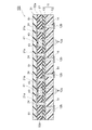
図1は、本発明による電子部品内蔵基板の第1実施形態の要部を示す概略断面図である。ワークシート100は、碁盤目状に2×2の配列で計4個の個別基板をシート面内に包含する電子部品内蔵集合基板であり、略矩形状の基体11の一方の面(図示上面)に絶縁層21,31を備え、絶縁層21の内部の所定位置に電子部品41及び板状枠部材51(部材)が埋設されたものである。
(First embodiment)
FIG. 1 is a schematic cross-sectional view showing a main part of a first embodiment of an electronic component built-in substrate according to the present invention. The
基体11は、絶縁層12の両面に配線層(パターン)12a,12bが形成されたものであり、配線層12a上に絶縁性の樹脂フィルムを真空圧着させることにより積層された絶縁層13を有している。配線層12aと配線層12bとは、絶縁層12を貫通するビア14を介して電気的に接続されている。また、絶縁層21の一方の面(図示上面)には、配線層21aが形成され、配線層12aと配線層21aとは、絶縁層13及び絶縁層21を貫通するビア24を介して電気的に接続されている。
The
絶縁層12,13に用いる材料は、シート状又はフィルム状に成型可能なものであれば特に制限されず使用可能であり、具体的には、例えば、ビニルベンジル樹脂、ポリビニルベンジルエーテル化合物樹脂、ビスマレイミドトリアジン樹脂(BTレジン)、ポリフェニレエーテル(ポリフェニレンエーテルオキサイド)樹脂(PPE,PPO)、シアネートエステル樹脂、エポキシ+活性エステル硬化樹脂、ポリフェニレンエーテル樹脂(ポリフェニレンオキサオド樹脂)、硬化性ポリオレフィン樹脂、ベンゾシクロブテン樹脂、ポリイミド樹脂、芳香族ポリエステル樹脂、芳香族液晶ポリエステル樹脂、ポリフェニレンサルファイド樹脂、ポリエーテルイミド樹脂、ポリアクリレート樹脂、ポリエーテルエーテルケトン樹脂、フッ素樹脂、エポキシ樹脂、フェノール樹脂又はベンゾオキサジン樹脂の単体、又は、これらの樹脂に、シリカ、タルク、炭酸カルシウム、炭酸マグネシウム、水酸化アルミニウム、水酸化マグネシウム、ホウ酸アルミウイスカ、チタン酸カリウム繊維、アルミナ、ガラスフレーク、ガラス繊維、窒化タンタル、窒化アルミニウム等を添加した材料、さらに、これらの樹脂に、マグネシウム、ケイ素、チタン、亜鉛、カルシウム、ストロンチウム、ジルコニウム、錫、ネオジウム、サマリウム、アルミニウム、ビスマス、鉛、ランタン、リチウム及びタンタルのうち少なくとも1種の金属を含む金属酸化物粉末を添加した材料、またさらには、これらの樹脂に、ガラス繊維、アラミド繊維等の樹脂繊維等を配合した材料、或いは、これらの樹脂をガラスクロス、アラミド繊維、不織布等に含浸させ材料、等を挙げることができ、電気特性、機械特性、吸水性、リフロー耐性等の観点から、適宜選択して用いることができる。
The material used for the insulating
絶縁層21,31は、熱硬化性樹脂からなり、その樹脂材料としては、例えば、エポキシ樹脂、フェノール樹脂、ビニルベンジルエーテル化合物樹脂、ビスマレイミドトリアジン樹脂、シアネートエステル系樹脂、ポリイミド、ポリオレフィン系樹脂、ポリエステル、ポリフェニレンオキサイド、液晶ポリマー、シリコーン樹脂、フッ素系樹脂等が挙げられ、これらを単独または複数組み合わせて使用することができる。また、アクリルゴム、エチレンアクリルゴム等のゴム材料や、ゴム成分を一部含むような樹脂材料であってもよい。さらに、これらの樹脂に、シリカ、タルク、炭酸カルシウム、炭酸マグネシウム、水酸化アルミニウム、水酸化マグネシウム、ホウ酸アルミウイスカ、チタン酸カリウム繊維、アルミナ、ガラスフレーク、ガラス繊維、窒化タンタル、窒化アルミニウム等を添加した材料、さらに、これらの樹脂に、マグネシウム、ケイ素、チタン、亜鉛、カルシウム、ストロンチウム、ジルコニウム、錫、ネオジウム、サマリウム、アルミニウム、ビスマス、鉛、ランタン、リチウム及びタンタルのうち少なくとも1種の金属を含む金属酸化物粉末を添加した材料、またさらには、これらの樹脂に、ガラス繊維、アラミド繊維等の樹脂繊維等を配合した材料、或いは、これらの樹脂をガラスクロス、アラミド繊維、不織布等に含浸させ材料、等を挙げることができ、電気特性、機械特性、吸水性、リフロー耐性等の観点から、適宜選択して用いることができる。 The insulating layers 21 and 31 are made of a thermosetting resin. Examples of the resin material include an epoxy resin, a phenol resin, a vinyl benzyl ether compound resin, a bismaleimide triazine resin, a cyanate ester resin, a polyimide, a polyolefin resin, Examples thereof include polyester, polyphenylene oxide, liquid crystal polymer, silicone resin, and fluorine resin, and these can be used alone or in combination. Further, it may be a rubber material such as acrylic rubber or ethylene acrylic rubber, or a resin material partially including a rubber component. In addition, silica, talc, calcium carbonate, magnesium carbonate, aluminum hydroxide, magnesium hydroxide, aluminum borate whisker, potassium titanate fiber, alumina, glass flake, glass fiber, tantalum nitride, aluminum nitride, etc. are added to these resins. In addition to the added materials, and these resins, at least one metal selected from magnesium, silicon, titanium, zinc, calcium, strontium, zirconium, tin, neodymium, samarium, aluminum, bismuth, lead, lanthanum, lithium and tantalum. Materials containing added metal oxide powders, or materials containing resin fibers such as glass fibers or aramid fibers, or glass resins, aramid fibers, nonwoven fabrics, etc., impregnated with these resins. Cite materials, etc. Can, electrical properties, mechanical properties, water absorption, from the viewpoint of reflow resistance, can be appropriately selected.
図2は、電子部品41の構造を概略的に示す斜視図である。この電子部品41は、ベアチップ状態の半導体IC(ダイ)であり、略矩形板状をなす主面41aに多数のランド電極42を有している。なお、図示においては、四隅にのみランド電極42及び後述するバンプ43(端子)を表示し、それ以外のランド電極42の表示を省略した。また、電子部品41の種類は、特に制限されるものではないが、例えば、CPUやDSPのように動作周波数が非常に高いデジタルICが挙げられる。
FIG. 2 is a perspective view schematically showing the structure of the
電子部品41の裏面41bは研磨されており、これにより電子部品41の厚さt1(主面41aから裏面41bまでの距離)は、通常の半導体ICに比して薄くされている。具体的には、電子部品41の厚さtは、例えば200μm以下、より好ましくは100μm以下、特に好ましくは20〜50μm程度とされる。また、電子部品41の裏面41bは、薄膜化或いは密着性を向上させるべく、エッチング、プラズマ処理、レーザ処理、ブラスト研磨、バフ研磨、薬品処理等による粗面化処理を行うことが好ましい。
The
なお、電子部品41の裏面41bの研磨は、ウェハの状態で多数の電子部品41に対して一括して行い、その後、ダイシングにより個別の電子部品41に分離することが好ましい。研磨により薄くする前にダイシングによって個別の電子部品41に切断分離した場合には、熱硬化性樹脂等により電子部品41の主面41aを覆った状態で裏面41bを研磨することもできる。
The
各ランド電極42には、導電性突起物の一種であるバンプ43(端子)が形成されている。バンプ43の種類は、特に制限されず、スタッドバンプ、プレートバンプ、メッキバンプ、ボールバンプ等の各種のバンプを例示できる。図示においては、スタッドバンプを例示した。バンプ43としてスタッドバンプを用いる場合には、銀(Ag)や銅(Cu)をワイヤボンディングにて形成することができ、プレートバンプを用いる場合には、メッキ、スパッタ又は蒸着によって形成することができる。また、メッキバンプを用いる場合には、メッキによって形成することができ、ボールバンプを用いる場合には、半田ボールをランド電極42上に載置した後、これを溶融させるか、クリーム半田をランド電極上に印刷した後、これを溶融させることによって形成することができる。また、導電性材料をスクリーン印刷し、これを硬化させた円錐状、円柱状等のバンプや、ナノペーストを印刷し、加熱によりこれを焼結させてなるバンプを用いることもできる。
Each
バンプ43に使用可能な金属種としては、特に限定されず、例えば、金(Au)、銀(Ag)、銅(Cu)、ニッケル(Ni)、スズ(Sn)、クロム(Cr)、ニッケル・クロム合金、半田等が挙げられ、これらのなかでは、接続性やマイグレーションを考慮すると金又は銅を用いることが好ましく、銅を用いることがより好ましい。バンプ43の材料として銅を用いると、例えば金を用いた場合に比して、ランド電極42に対する高い接合強度を得ることが可能となり、電子部品41自体の信頼性が高められる。
The metal species that can be used for the
バンプ43の寸法形状は、ランド電極42間の間隔(ピッチ)に応じて適宜設定することができ、例えば、ランド電極42のピッチが約100μmである場合には、バンプ43の最大径を10〜90μm程度、高さを2〜100μm程度にすればよい。なお、バンプ43は、ウェハのダイシングにより個別の電子部品41に切断分離した後、ワイヤボンダーを用いて各ランド電極42に接合することができる。
The size and shape of the
図3は、板状枠部材51の構造を概略的に示す斜視図である。本実施形態で用いる板状枠部材51は、4つの窓Wが区画された格子状の枠部52からなる。枠部52の外形は、基体11の外形と略相似の略矩形状であり、その外寸が基体11より若干小さく設計されている。また、枠部52は、枠外周に向かって傾斜する傾斜面52aを有し、これにより、枠部52は、枠外周に向かって厚さが薄くなっている。また、枠部52の厚さt2(最厚部)は、電子部品41の厚さt1よりも僅かに薄い程度が好ましい。
FIG. 3 is a perspective view schematically showing the structure of the plate-
板状枠部材51に使用可能な材料としては、下記式(1);
α1 < α3 且つ α2 < α3 ・・・ (1)、
((式中、α1は、電子部品41の線熱膨張係数(ppm/K)を示し、α2は、板状枠部材51の線熱膨張係数(ppm/K)を示し、α3は、上記の基体11、各配線層又は各絶縁層の線熱膨張係数(ppm/K)を示す。)を満たすものであれば、特に制限なく用いることができる。この種の用途に用いられる電子部品、基体、配線層及び絶縁層においては、一般的に、α1が1〜8(ppm/K)程度でありα3が14〜20(ppm/K)程度であるので、α2は、3〜16(ppm/K)であることが好ましい。より具体的には、線熱膨張係数が3〜16(ppm/K)の金属、合金及び樹脂等が挙げられ、例えば、SUS400(11ppm/K)、SUS410(11ppm/K)、SUS430(10.5ppm/K)、SUS630(11ppm/K)、SUS631(10ppm/K)、SUS316(16ppm/K)、42アロイ(4.5ppm/K)、インコネル(14ppm/K)、ニッケル(12.5ppm/K)、ニッケルクロムモリブデン鋼(11ppm/K)、鉄(11ppm/K)、鋳鉄(10ppm/K)、チタン(9ppm/K)、芳香族ポリアミド(製品名:ミクトロンGQ;13ppm/K)、芳香族ポリアミド(製品名:ミクトロンML;3ppm/K)、PET(15ppm/K)、ポリイミド(3〜15ppm/K)等が挙げられ、これらの中でも、加工性や入手性、剛直性、コスト等の観点から、SUS430又はインコネルを用いることが好ましく、これらのなかでは、SUS430を用いることがより好ましい。
As a material that can be used for the plate-
α1 <α3 and α2 <α3 (1),
( Where α1 represents the linear thermal expansion coefficient (ppm / K) of the
以下、図4乃至図14を参照しながら、上記のワークシート100として、電子部品41を3つ内蔵する個別基板を、計4つ包含するものの製造方法について説明する。
Hereinafter, a manufacturing method of the above-described
まず、両面銅張ガラスエポキシをドリル穿孔し、さらに無電解メッキ、電解メッキを施した後、不要部分をエッチングにより除去する等の公知の手法を用いて、配線層(パターン)12a,12b及びビア14が形成された基体11を準備する(図4)。ここでは、配線層12a,12b及びビア14からなる回路構成を、板状枠部材51の各窓Wと対応する4箇所に各々離間して形成する。そしてさらに、基体11の配線層12a上に絶縁層13を形成する(図5)。その後、上記の操作により得られる基体11を、図示しないステンレス製のワークステージ上の所定位置に載置固定し、以降の工程を行う。
First, the wiring layers (patterns) 12a and 12b and vias are formed using a known technique such as drilling a double-sided copper-clad glass epoxy, further electroless plating and electrolytic plating, and then removing unnecessary portions by etching. A base 11 on which 14 is formed is prepared (FIG. 4). Here, the circuit configuration including the wiring layers 12 a and 12 b and the
次に、基体11の絶縁層13上の製品エリアS1〜S4内の所定位置に、電子部品41を載置する(図6及び図7)。ここで、製品エリアS1〜S4は、配線層12a,12b及びビア14等の回路構成に基づいて画定される、個別基板の作製領域である。ここでは、上述したように、基体11に板状枠部材51の各窓Wと対応する4箇所に同一の回路構成が4つ形成されているので、これに対応して、2×2の碁盤目状に各々離間して配列された製品エリアS1〜S4及び格子状の非製品エリアT(製品エリアS1〜S4を除く領域)が画定されている(図6)。
Next, the
さらに、基体11の絶縁層13上に、板状枠部材51を載置する(図8乃至図10)。ここでは、板状枠部材51を、板状枠部材51の各窓Wが製品エリアS1〜S4と一致するように、電子部品41の非載置部である非製品エリアTの所定位置に載置する。かくして、板状枠部材51は、電子部品41を取り囲むように載置される(図8乃至図10)。また、電子部品41と板状枠部材51とは、基体11の絶縁層13上の同一平面に載置される(図9及び図10)。なお、板状枠部材51の載置は、電子部品41の載置に先行して行っても、電子部品41の載置と同時に行なっても構わない。
Further, the plate-
その後、上記のように基体11の絶縁層13上に載置された電子部品41及び板状枠部材51を覆うように、絶縁層21を形成する(図11)。具体的には、未硬化又は半硬化状態の熱硬化性樹脂を、基体11の絶縁層13上に塗布し、熱を印加し硬化させることにより絶縁層21を形成する。
Thereafter, the insulating
次に、絶縁層21の一部を除去して、電子部品41のバンプ43を露出させる(図12)。この絶縁層21の除去方法は、公知の手法を適宜選択することができ、具体的には、例えば、グラインダーを用いた研磨や、ブラスト処理、炭酸ガスレーザの照射等が挙げられる。
Next, a part of the insulating
そして、公知の手法により、絶縁層13,21を貫通するビア24を各々形成し(図13)、次いで、サブトラクティブ法又はアディティブ法等の公知の手法により、絶縁層31上に配線層21aを形成することにより、電子部品41、バンプ43、配線層21a及び12aを、ビア24を介して電気的に接続する(図14)。
Then, vias 24 penetrating the insulating
その後、定法にしたがい、絶縁層21上に絶縁層31を形成することで、図1に示す構成のワークシート100を得る。好ましくは、上述した絶縁層21と同様に、熱硬化性樹脂である絶縁性エポキシ樹脂を絶縁層21上に塗布し、熱を印加し硬化させることにより、絶縁層31を形成する。
Thereafter, in accordance with a regular method, the insulating
ここで、絶縁層21,31の形成は、未硬化又は半硬化状態の熱硬化性樹脂を塗布した後、熱を印加して半硬化させた後、プレス手段を用いて硬化成形することが好ましい。このようにすると、配線層12a,12b,21a、絶縁層12,13,21,31、電子部品41、板状枠部材51間の密着性が向上する。この硬化成形は、必要に応じ熱を印加しながら行ってもよい。すなわち、絶縁層21,31の形成には、種々の公知の手段を採用することができ、例えば、スクリーン印刷、スピンコーター等の手法の他、プレス、真空ラミネート、常圧ラミネート等も採用可能である。
Here, the insulating
また、電子部品41の厚さt1よりも薄く、枠外周に向かって傾斜する傾斜面52aを有する板状枠部材51を用いた場合は、基体11の外周方向へ向かって板状枠部材51の厚さが低減する、言いえれば、絶縁層21中で占有する空間体積率が基体11の外周方向に向かって低減するので、硬化プレス成形時に、未硬化(半硬化)樹脂が製品エリアS1〜S4から非製品エリアTを通過して基体11の外周方向へと流動し易くなる。よって、製品エリアS1〜S4に圧力を均等に印加させ易くなり、配線層12a,12b,21a、絶縁層12,13,21,31、電子部品41、板状枠部材51間の密着性が向上するとともに、ワークシート100厚さ、製品エリアS1〜S4の厚みの均等性及び平坦性が向上される。さらには、配線層12a,12b,21a、絶縁層12,13,21,31、電子部品41、板状枠部材51間に存在・混入し得る気泡が効率的に排除される等して製造加工トラブルの発生を抑制でき、歩留まり及び実装信頼性を向上させることができる。
Further, when the plate-
そして、上記のワークシート100を、ダイシング等の公知の手法によって、製品エリアS1〜S4毎に分割することにより、各々の個別基板200(電子部品内蔵基板)が得られる(図15)。そして、得られた個別基板200に、所望の電子部品を表面実装することにより、電子部品内蔵モジュール(電子部品内蔵基板)が得られる。その一例として、配線層61a及び絶縁層31を貫通するビア34を形成するとともに抵抗やキャパシタ等の受動部品61を設置した、電子部品内蔵モジュール201を図示する(図16)。
Then, the individual substrate 200 (electronic component built-in substrate) is obtained by dividing the
さて、上述したワークシート100の製造方法においては、線熱膨張係数が上記式(1)を満たす板状枠部材51を非製品エリアTに配置するので、製品エリアS1〜S4と非製品エリアTとの間の熱膨張及び熱収縮の度合いの差異が低減され、絶縁層21,31形成時に発生する不均一な内部応力が緩和される。また、板状枠部材51は、応力印加に抗して基板の形状変化を緩和する内部構造体として機能するので、基板強度が向上する。したがって、基板の反りの発生を効果的に抑制できる。
Now, in the manufacturing method of the
また、板状枠部材51は、内部構造体として基板の形状変化を緩和する。したがって、配線層21aや絶縁層31のビルドアップ時、又は、受動部品61の表面実装時等において、所望しない応力印加に抗して反りの発生を抑制できる。
Further, the plate-
さらに、電子部品41を取り囲むように板状枠部材51を載置するので、シート面内において方向異方性なく熱膨張及び熱収縮の度合いを漸近でき、方向異方性なく基板強度を向上できる。
In addition, since the plate-
しかも、板状枠部材51を電子部品41と同一平面に配置するので、基体11厚さ方向の不均一な応力印加を緩和でき、反りの発生をより一層効果的に抑制できる。
Moreover, since the plate-
一方、得られるワークシート100は、反りが抑制され基板強度が向上されたものとなるので、搬送、ビルドアップ、表面実装等の製造加工時のハンドリング性が向上したものとなる。よって、かかるワークシート100を用いることにより、以降における製造加工トラブルの発生を抑制できるようになり、歩留まりが向上するとともに、実装信頼性が向上する。
On the other hand, since the obtained
(第2実施形態)
図17は、本発明による電子部品内蔵基板の第2実施形態の概略構成を示す平面図である。ワークシート300は、板状枠部材51に代えて、上記式(1)を満たす部材81を備えること以外は、上記の第1実施形態のワークシート100と同様に構成されたものである。部材81は、断面矩形の板部材82と、断面矩形の十字状の板部材83とから構成されており、図示の如く、複数の板部材82が基体11の周縁領域に枠状に配置され、その枠内に十字状の板部材83が配置されている。また、板部材82は、板部材83よりも厚さが薄くされている。
(Second Embodiment)
FIG. 17 is a plan view showing a schematic configuration of the second embodiment of the electronic component built-in substrate according to the present invention. The
このような部材81を用いても、上記第1実施形態と同様の作用効果が奏されるとともに、部材81が、直状をなす板部材82及び板部材83から分割構成されているので、部材81のハンドリング性及び汎用性が高められ、生産性の向上へ寄与できる。
Even if such a
(第3実施形態)
図18及び図19は、本発明による電子部品内蔵基板の第3実施形態の概略構成を示す平面図及び部分断面図である。ワークシート400は、板状枠部材51に代えて、上記式(1)を満たす部材84を備えること以外は、上記の第1実施形態のワークシート100と同様に構成されたものである。部材84は、粗面化された面85aに種々複数の貫通孔85b(凹部)が形成された枠部材85と、断面矩形の板部材86とから構成されており、図示の如く、枠部材85の枠内に板部材86が配置されたものである。ここで、図18においては、理解を容易にするために、貫通孔85bの表示を省略している。枠部材85の面85aに設けられた貫通孔85bは、基体11の外周方向へ向かって凹部体積(内容積)が増大するように配設されている。
(Third embodiment)
18 and 19 are a plan view and a partial cross-sectional view showing a schematic configuration of the third embodiment of the electronic component built-in substrate according to the present invention. The
このような部材84を用いても、上記第1及び第2実施形態と同様の作用効果が奏される。しかも、部材84が粗面化された面85aを有するので、絶縁層21との密着性が高められ、部材84の浮きや剥がれによる取り扱い時の強度低下や、切り出し時の絶縁層13,21の脱落や飛び散りを低下させることができ、取り扱い性の向上に寄与できる。なお、図20に示すように、貫通孔85bに代えて、非貫通の孔85c(窪み、凹部)を形成してもよい。
Even when such a
なお、上記第1乃至第3実施形態では、電子部品41として半導体ICを内蔵する集合基板及び個別基板を説明したが、本発明は、かかる半導体ICに代えて及び/又はかかる半導体ICとともに、バリスタ、抵抗、コンデンサ、インダクタ、フィルタ、アンテナ、トランス等の電子部品を内蔵するものであっても同様に実施することができる。
In the first to third embodiments, the collective substrate and the individual substrate in which the semiconductor IC is incorporated as the
以上説明した通り、本発明の電子部品内蔵基板及びその製造方法によれば、煩雑な工程を必要とせず低コストで且つ簡易な構成で、熱印加時に発生する不均一な内部応力を緩和し且つ基板強度を向上させることができ、これにより、反りの発生を効果的に抑制でき、生産性及び経済性並びに製品の信頼性を向上させることができるので、電子部品をモジュール化する際の更なる薄膜化に資することができるとともに、薄膜型の電子部品を内蔵する電子機器、装置、システム、各種デバイス等、特に小型化、薄膜化及び高性能化が要求されるもの、並びにそれらの製造に広く且つ有効に利用することができる。 As described above, according to the electronic component built-in substrate and the manufacturing method thereof of the present invention, it is possible to relieve uneven internal stress generated at the time of heat application with a low-cost and simple configuration without requiring a complicated process and The board strength can be improved, which can effectively suppress the occurrence of warpage, and can improve productivity, economy and product reliability. Can contribute to thinning, and electronic devices, devices, systems, various devices with built-in thin-film electronic components, especially those that require miniaturization, thinning and high performance, and a wide range of their production And it can be used effectively.
11…基体、12,13,21,31…絶縁層、12a,12b,21a,61a…配線層、14,24,34…ビア、41…電子部品、41a…主面、41b…裏面、42…ランド電極、43…バンプ、51…板状枠部材(部材)、52…枠部、52a…傾斜面、61…受動部品、81…部材、82…板部材、83…板部材、84…部材、85…枠部材、85a…面、85b…貫通孔(凹部)、85c…非貫通の孔(窪み、凹部)、86…板部材、100,300,400…ワークシート(電子部品内蔵基板)、200…個別基板(電子部品内蔵基板)、201…電子部品内蔵モジュール(電子部品内蔵基板)。
DESCRIPTION OF
Claims (4)
前記基体上に電子部品を載置する工程と、
前記基体における前記電子部品の非載置部に、下記式(1);
α1 < α3 且つ α2 < α3 ・・・ (1)、
α1 : 電子部品の線熱膨張係数(ppm/K)
α2 : 部材の線熱膨張係数(ppm/K)
α3 : 基体、配線層又は絶縁層の線熱膨張係数(ppm/K)
(式中、α1 < α3は、電子部品の線熱膨張係数の値が、基体の線熱膨張係数の値、配線層の線熱膨張係数の値、及び、絶縁層の線熱膨張係数の値のうちいずれか1つの値よりも小さいことを意味し、α2 < α3は、部材の線熱膨張係数の値が、基体の線熱膨張係数の値、配線層の線熱膨張係数の値、及び、絶縁層の線熱膨張係数の値のうちいずれか1つの値よりも小さいことを意味する。)
で表される関係を満たす部材を載置する工程と、
前記基体上に、前記電子部品及び前記部材を覆うように、前記絶縁層を形成する工程と、
前記基体及び/又は絶縁層に配線層を形成する工程と、
を有し、
前記部材として、前記絶縁層中で占有する空間体積率が前記基体の外周方向に向かって小さくなるものを用いる、
電子部品内蔵基板の製造方法。 Preparing a substrate;
Placing an electronic component on the substrate;
In the non-mounting portion of the electronic component on the base, the following formula (1);
α1 <α3 and α2 <α3 (1),
α1: Linear thermal expansion coefficient of electronic parts (ppm / K)
α2: Linear thermal expansion coefficient of member (ppm / K)
α3: Coefficient of linear thermal expansion (ppm / K) of the substrate, wiring layer or insulating layer
(Where α1 <α3 is the value of the linear thermal expansion coefficient of the electronic component, the value of the linear thermal expansion coefficient of the substrate, the value of the linear thermal expansion coefficient of the wiring layer, and the value of the linear thermal expansion coefficient of the insulating layer) Means that the value of the linear thermal expansion coefficient of the member is the value of the linear thermal expansion coefficient of the substrate, the value of the linear thermal expansion coefficient of the wiring layer, and This means that it is smaller than any one of the values of the coefficient of linear thermal expansion of the insulating layer.)
A step of placing a member satisfying the relationship represented by:
Forming the insulating layer on the base so as to cover the electronic component and the member;
Forming a wiring layer on the substrate and / or insulating layer;
Have
As the member, use those pre Symbol spatial volume ratio occupied in the insulating layer is reduced toward the outer peripheral direction of the substrate,
Manufacturing method of electronic component built-in substrate.
請求項1に記載の電子部品内蔵基板の製造方法。 In the step of placing the member, the member is placed so as to surround the electronic component.
The manufacturing method of the electronic component built-in substrate according to claim 1.
請求項1又は2に記載の電子部品内蔵基板の製造方法。 In the step of placing the member, the electronic component and the member are placed on substantially the same plane.
The manufacturing method of the electronic component built-in substrate according to claim 1 or 2.
前記基体上に載置された電子部品と、
前記基体における前記電子部品の非載置部に載置されており、且つ、下記式(1);
α1 < α3 且つ α2 < α3 ・・・ (1)、
α1 : 電子部品の線熱膨張係数(ppm/K)
α2 : 部材の線熱膨張係数(ppm/K)
α3 : 基体、配線層又は絶縁層の線熱膨張係数(ppm/K)
(式中、α1 < α3は、電子部品の線熱膨張係数の値が、基体の線熱膨張係数の値、配線層の線熱膨張係数の値、及び、絶縁層の線熱膨張係数の値のうちいずれか1つの値よりも小さいことを意味し、α2 < α3は、部材の線熱膨張係数の値が、基体の線熱膨張係数の値、配線層の線熱膨張係数の値、及び、絶縁層の線熱膨張係数の値のうちいずれか1つの値よりも小さいことを意味する。)
で表される関係を満たす部材と、
前記基体上に、前記電子部品及び前記部材を覆うように形成された前記絶縁層と、
前記基体及び/又は絶縁層に形成された配線層と、
を有し、
前記部材は、前記絶縁層中で占有する空間体積率が前記基体の外周方向に向かって小さくなる、
電子部品内蔵基板。 A substrate;
An electronic component placed on the substrate;
It is mounted on the non-mounting portion of the electronic component on the base, and the following formula (1);
α1 <α3 and α2 <α3 (1),
α1: Linear thermal expansion coefficient of electronic parts (ppm / K)
α2: Linear thermal expansion coefficient of member (ppm / K)
α3: Coefficient of linear thermal expansion (ppm / K) of the substrate, wiring layer or insulating layer
(Where α1 <α3 is the value of the linear thermal expansion coefficient of the electronic component, the value of the linear thermal expansion coefficient of the substrate, the value of the linear thermal expansion coefficient of the wiring layer, and the value of the linear thermal expansion coefficient of the insulating layer) Means that the value of the linear thermal expansion coefficient of the member is the value of the linear thermal expansion coefficient of the substrate, the value of the linear thermal expansion coefficient of the wiring layer, and This means that it is smaller than any one of the values of the coefficient of linear thermal expansion of the insulating layer.)
A member satisfying the relationship represented by
On the base, the insulating layer formed to cover the electronic component and the member;
A wiring layer formed on the substrate and / or the insulating layer;
Have
The member, the spatial volume ratio occupied in the previous SL insulating layer is smaller toward the outer peripheral direction of the substrate,
Electronic component built-in substrate.
Priority Applications (5)
| Application Number | Priority Date | Filing Date | Title |
|---|---|---|---|
| JP2007193836A JP4518113B2 (en) | 2007-07-25 | 2007-07-25 | Electronic component built-in substrate and manufacturing method thereof |
| US12/219,355 US8237059B2 (en) | 2007-07-25 | 2008-07-21 | Electronic component-embedded board and method of manufacturing the same |
| EP08013361A EP2019571B1 (en) | 2007-07-25 | 2008-07-24 | Electronic component-embedded board and method of manufacturing the same |
| CN2008101442136A CN101355858B (en) | 2007-07-25 | 2008-07-25 | Electronic component-embedded board and method of manufacturing the same |
| US13/533,176 US20120285013A1 (en) | 2007-07-25 | 2012-06-26 | Electronic Component-Embedded Board and Method of Manufacturing the Same |
Applications Claiming Priority (1)
| Application Number | Priority Date | Filing Date | Title |
|---|---|---|---|
| JP2007193836A JP4518113B2 (en) | 2007-07-25 | 2007-07-25 | Electronic component built-in substrate and manufacturing method thereof |
Publications (2)
| Publication Number | Publication Date |
|---|---|
| JP2009032823A JP2009032823A (en) | 2009-02-12 |
| JP4518113B2 true JP4518113B2 (en) | 2010-08-04 |
Family
ID=40011038
Family Applications (1)
| Application Number | Title | Priority Date | Filing Date |
|---|---|---|---|
| JP2007193836A Active JP4518113B2 (en) | 2007-07-25 | 2007-07-25 | Electronic component built-in substrate and manufacturing method thereof |
Country Status (4)
| Country | Link |
|---|---|
| US (2) | US8237059B2 (en) |
| EP (1) | EP2019571B1 (en) |
| JP (1) | JP4518113B2 (en) |
| CN (1) | CN101355858B (en) |
Families Citing this family (17)
| Publication number | Priority date | Publication date | Assignee | Title |
|---|---|---|---|---|
| JP4518113B2 (en) * | 2007-07-25 | 2010-08-04 | Tdk株式会社 | Electronic component built-in substrate and manufacturing method thereof |
| US8921705B2 (en) * | 2008-11-28 | 2014-12-30 | Ibiden Co., Ltd. | Wiring board and fabrication method therefor |
| US8945329B2 (en) * | 2011-06-24 | 2015-02-03 | Ibiden Co., Ltd. | Printed wiring board and method for manufacturing printed wiring board |
| JP2015018979A (en) * | 2013-07-12 | 2015-01-29 | イビデン株式会社 | Printed wiring board |
| KR102250997B1 (en) | 2014-05-02 | 2021-05-12 | 삼성전자주식회사 | Semiconductor package |
| WO2016098865A1 (en) * | 2014-12-19 | 2016-06-23 | 富士フイルム株式会社 | Multilayer wiring substrate |
| KR101602377B1 (en) | 2015-08-13 | 2016-03-15 | 주식회사 이오비스 | 3D shape measuring method |
| DE102016212129B4 (en) * | 2016-07-04 | 2022-05-19 | Schweizer Electronic Ag | Radio frequency transmission/reception element and method of manufacturing a radio frequency transmission/reception element |
| TWI645973B (en) | 2017-12-15 | 2019-01-01 | 律勝科技股份有限公司 | Polyimide thinned flexible substrate and manufacturing method thereof |
| WO2020067320A1 (en) * | 2018-09-27 | 2020-04-02 | 株式会社村田製作所 | Resin multilayer substrate |
| CN111511104B (en) * | 2019-01-31 | 2024-05-28 | 奥特斯奥地利科技与系统技术有限公司 | Component carrier and method for producing a component carrier |
| US11277917B2 (en) | 2019-03-12 | 2022-03-15 | Advanced Semiconductor Engineering, Inc. | Embedded component package structure, embedded type panel substrate and manufacturing method thereof |
| JP7380681B2 (en) * | 2019-04-26 | 2023-11-15 | Tdk株式会社 | Collective board and its manufacturing method |
| US11296030B2 (en) | 2019-04-29 | 2022-04-05 | Advanced Semiconductor Engineering, Inc. | Embedded component package structure and manufacturing method thereof |
| US10950551B2 (en) | 2019-04-29 | 2021-03-16 | Advanced Semiconductor Engineering, Inc. | Embedded component package structure and manufacturing method thereof |
| US11778752B2 (en) * | 2020-01-21 | 2023-10-03 | Avary Holding (Shenzhen) Co., Limited. | Circuit board with embedded electronic component and method for manufacturing the same |
| US11848280B2 (en) * | 2020-11-25 | 2023-12-19 | ADVANCED SEMlCONDUCTOR ENGINEERING, INC. | Method for manufacturing assembly structure by using frame structure on substrate |
Family Cites Families (24)
| Publication number | Priority date | Publication date | Assignee | Title |
|---|---|---|---|---|
| JPH0770645B2 (en) | 1986-06-11 | 1995-07-31 | 日本電気株式会社 | Hybrid integrated circuit |
| US5233222A (en) * | 1992-07-27 | 1993-08-03 | Motorola, Inc. | Semiconductor device having window-frame flag with tapered edge in opening |
| JP3447029B2 (en) | 1995-11-07 | 2003-09-16 | イビデン株式会社 | Printed wiring board manufacturing method |
| US5844319A (en) * | 1997-03-03 | 1998-12-01 | Motorola Corporation | Microelectronic assembly with collar surrounding integrated circuit component on a substrate |
| JP3921756B2 (en) * | 1997-10-06 | 2007-05-30 | 株式会社デンソー | Printed circuit board and manufacturing method thereof |
| JP3659167B2 (en) | 1999-04-16 | 2005-06-15 | 松下電器産業株式会社 | Module parts and manufacturing method thereof |
| JP3619395B2 (en) * | 1999-07-30 | 2005-02-09 | 京セラ株式会社 | Semiconductor device built-in wiring board and manufacturing method thereof |
| US6842974B1 (en) * | 1999-09-27 | 2005-01-18 | Matsushita Electric Industrial Co., Ltd. | Component mounting method and component mounting apparatus |
| JP2001284783A (en) * | 2000-03-30 | 2001-10-12 | Shinko Electric Ind Co Ltd | Substrate for surface-mounting and surface-mounting structure |
| JP2002016173A (en) * | 2000-06-30 | 2002-01-18 | Mitsubishi Electric Corp | Semiconductor device |
| JP3816380B2 (en) | 2001-12-14 | 2006-08-30 | 富士通株式会社 | Substrate unit provided with heat-absorbing dummy component and method for manufacturing the same |
| JP4026705B2 (en) * | 2002-05-27 | 2007-12-26 | Tdk株式会社 | Layer constituting multilayer electronic component and method of manufacturing multilayer electronic component |
| JP2003347741A (en) * | 2002-05-30 | 2003-12-05 | Taiyo Yuden Co Ltd | Composite multilayer substrate and module using the same |
| JP2004071698A (en) * | 2002-08-02 | 2004-03-04 | Hitachi Metals Ltd | Semiconductor package |
| JP3951854B2 (en) * | 2002-08-09 | 2007-08-01 | カシオ計算機株式会社 | Semiconductor device and manufacturing method thereof |
| US7394663B2 (en) * | 2003-02-18 | 2008-07-01 | Matsushita Electric Industrial Co., Ltd. | Electronic component built-in module and method of manufacturing the same |
| JP4194408B2 (en) * | 2003-04-03 | 2008-12-10 | 日本特殊陶業株式会社 | Substrate with reinforcing material, wiring substrate comprising semiconductor element, reinforcing material and substrate |
| JP4135565B2 (en) * | 2003-06-06 | 2008-08-20 | 松下電器産業株式会社 | Electronic circuit device and manufacturing method thereof |
| JP2005167141A (en) | 2003-12-05 | 2005-06-23 | Ibiden Co Ltd | Method of manufacturing printed wiring board and multilayer printed wiring board |
| JP2005251792A (en) * | 2004-03-01 | 2005-09-15 | Fujitsu Ltd | Wiring board and manufacturing method thereof |
| JP3914239B2 (en) * | 2005-03-15 | 2007-05-16 | 新光電気工業株式会社 | Wiring board and method for manufacturing wiring board |
| JP4526983B2 (en) * | 2005-03-15 | 2010-08-18 | 新光電気工業株式会社 | Wiring board manufacturing method |
| US8829661B2 (en) * | 2006-03-10 | 2014-09-09 | Freescale Semiconductor, Inc. | Warp compensated package and method |
| JP4518113B2 (en) * | 2007-07-25 | 2010-08-04 | Tdk株式会社 | Electronic component built-in substrate and manufacturing method thereof |
-
2007
- 2007-07-25 JP JP2007193836A patent/JP4518113B2/en active Active
-
2008
- 2008-07-21 US US12/219,355 patent/US8237059B2/en active Active
- 2008-07-24 EP EP08013361A patent/EP2019571B1/en active Active
- 2008-07-25 CN CN2008101442136A patent/CN101355858B/en active Active
-
2012
- 2012-06-26 US US13/533,176 patent/US20120285013A1/en not_active Abandoned
Also Published As
| Publication number | Publication date |
|---|---|
| JP2009032823A (en) | 2009-02-12 |
| CN101355858B (en) | 2011-04-06 |
| US20090025971A1 (en) | 2009-01-29 |
| EP2019571B1 (en) | 2012-09-05 |
| EP2019571A3 (en) | 2010-04-14 |
| EP2019571A2 (en) | 2009-01-28 |
| US8237059B2 (en) | 2012-08-07 |
| US20120285013A1 (en) | 2012-11-15 |
| CN101355858A (en) | 2009-01-28 |
Similar Documents
| Publication | Publication Date | Title |
|---|---|---|
| JP4518113B2 (en) | Electronic component built-in substrate and manufacturing method thereof | |
| JP4518114B2 (en) | Electronic component built-in substrate and manufacturing method thereof | |
| JP4487271B2 (en) | Collective substrate and manufacturing method thereof | |
| JP5540276B2 (en) | Electronic component built-in substrate and manufacturing method thereof | |
| JP3945483B2 (en) | Manufacturing method of semiconductor device | |
| CN1269199C (en) | Flip chip type semiconductor device and making method thereof | |
| CN106328607B (en) | Semiconductor device and method for manufacturing the same | |
| JP5441007B2 (en) | Manufacturing method of electronic component built-in substrate | |
| US8421204B2 (en) | Embedded semiconductor power modules and packages | |
| JP2011151048A (en) | Method of manufacturing electronic component, and electronic component | |
| JP5098313B2 (en) | Wiring board | |
| JP2005123493A (en) | Wiring substrate and element packaging substrate | |
| JP5013138B2 (en) | Collective substrate and manufacturing method thereof | |
| JP5097006B2 (en) | Printed wiring board and manufacturing method thereof | |
| JP2014027311A (en) | Method for manufacturing electronic component built-in substrate | |
| JP2005191157A (en) | Semiconductor device and manufacturing method thereof | |
| JP4209341B2 (en) | Semiconductor device and manufacturing method thereof | |
| JP2008021944A (en) | Multilayer wiring board and manufacturing method thereof | |
| JP2013062424A (en) | Manufacturing method of semiconductor device and semiconductor device manufactured by the same |
Legal Events
| Date | Code | Title | Description |
|---|---|---|---|
| A621 | Written request for application examination |
Free format text: JAPANESE INTERMEDIATE CODE: A621 Effective date: 20090324 |
|
| A977 | Report on retrieval |
Free format text: JAPANESE INTERMEDIATE CODE: A971007 Effective date: 20090716 |
|
| A131 | Notification of reasons for refusal |
Free format text: JAPANESE INTERMEDIATE CODE: A131 Effective date: 20090721 |
|
| A521 | Request for written amendment filed |
Free format text: JAPANESE INTERMEDIATE CODE: A523 Effective date: 20090915 |
|
| A131 | Notification of reasons for refusal |
Free format text: JAPANESE INTERMEDIATE CODE: A131 Effective date: 20100305 |
|
| A521 | Request for written amendment filed |
Free format text: JAPANESE INTERMEDIATE CODE: A523 Effective date: 20100408 |
|
| TRDD | Decision of grant or rejection written | ||
| A01 | Written decision to grant a patent or to grant a registration (utility model) |
Free format text: JAPANESE INTERMEDIATE CODE: A01 Effective date: 20100427 |
|
| A01 | Written decision to grant a patent or to grant a registration (utility model) |
Free format text: JAPANESE INTERMEDIATE CODE: A01 |
|
| A61 | First payment of annual fees (during grant procedure) |
Free format text: JAPANESE INTERMEDIATE CODE: A61 Effective date: 20100510 |
|
| FPAY | Renewal fee payment (event date is renewal date of database) |
Free format text: PAYMENT UNTIL: 20130528 Year of fee payment: 3 |
|
| R150 | Certificate of patent or registration of utility model |
Ref document number: 4518113 Country of ref document: JP Free format text: JAPANESE INTERMEDIATE CODE: R150 Free format text: JAPANESE INTERMEDIATE CODE: R150 |
|
| FPAY | Renewal fee payment (event date is renewal date of database) |
Free format text: PAYMENT UNTIL: 20140528 Year of fee payment: 4 |
|
| R250 | Receipt of annual fees |
Free format text: JAPANESE INTERMEDIATE CODE: R250 |