EP1535192B1 - Gatterprozessor - Google Patents
Gatterprozessor Download PDFInfo
- Publication number
- EP1535192B1 EP1535192B1 EP03765145A EP03765145A EP1535192B1 EP 1535192 B1 EP1535192 B1 EP 1535192B1 EP 03765145 A EP03765145 A EP 03765145A EP 03765145 A EP03765145 A EP 03765145A EP 1535192 B1 EP1535192 B1 EP 1535192B1
- Authority
- EP
- European Patent Office
- Prior art keywords
- row
- processor
- buses
- array
- functionality
- Prior art date
- Legal status (The legal status is an assumption and is not a legal conclusion. Google has not performed a legal analysis and makes no representation as to the accuracy of the status listed.)
- Expired - Lifetime
Links
Images


Classifications
-
- G—PHYSICS
- G06—COMPUTING; CALCULATING OR COUNTING
- G06F—ELECTRIC DIGITAL DATA PROCESSING
- G06F11/00—Error detection; Error correction; Monitoring
- G06F11/07—Responding to the occurrence of a fault, e.g. fault tolerance
- G06F11/16—Error detection or correction of the data by redundancy in hardware
- G06F11/20—Error detection or correction of the data by redundancy in hardware using active fault-masking, e.g. by switching out faulty elements or by switching in spare elements
- G06F11/202—Error detection or correction of the data by redundancy in hardware using active fault-masking, e.g. by switching out faulty elements or by switching in spare elements where processing functionality is redundant
- G06F11/2051—Error detection or correction of the data by redundancy in hardware using active fault-masking, e.g. by switching out faulty elements or by switching in spare elements where processing functionality is redundant in regular structures
-
- G—PHYSICS
- G06—COMPUTING; CALCULATING OR COUNTING
- G06F—ELECTRIC DIGITAL DATA PROCESSING
- G06F11/00—Error detection; Error correction; Monitoring
- G06F11/07—Responding to the occurrence of a fault, e.g. fault tolerance
- G06F11/16—Error detection or correction of the data by redundancy in hardware
- G06F11/20—Error detection or correction of the data by redundancy in hardware using active fault-masking, e.g. by switching out faulty elements or by switching in spare elements
- G06F11/202—Error detection or correction of the data by redundancy in hardware using active fault-masking, e.g. by switching out faulty elements or by switching in spare elements where processing functionality is redundant
- G06F11/2038—Error detection or correction of the data by redundancy in hardware using active fault-masking, e.g. by switching out faulty elements or by switching in spare elements where processing functionality is redundant with a single idle spare processing component
-
- G—PHYSICS
- G06—COMPUTING; CALCULATING OR COUNTING
- G06F—ELECTRIC DIGITAL DATA PROCESSING
- G06F15/00—Digital computers in general; Data processing equipment in general
- G06F15/76—Architectures of general purpose stored program computers
- G06F15/80—Architectures of general purpose stored program computers comprising an array of processing units with common control, e.g. single instruction multiple data processors
- G06F15/8007—Architectures of general purpose stored program computers comprising an array of processing units with common control, e.g. single instruction multiple data processors single instruction multiple data [SIMD] multiprocessors
- G06F15/8023—Two dimensional arrays, e.g. mesh, torus
-
- G—PHYSICS
- G06—COMPUTING; CALCULATING OR COUNTING
- G06F—ELECTRIC DIGITAL DATA PROCESSING
- G06F11/00—Error detection; Error correction; Monitoring
- G06F11/07—Responding to the occurrence of a fault, e.g. fault tolerance
- G06F11/16—Error detection or correction of the data by redundancy in hardware
- G06F11/20—Error detection or correction of the data by redundancy in hardware using active fault-masking, e.g. by switching out faulty elements or by switching in spare elements
- G06F11/202—Error detection or correction of the data by redundancy in hardware using active fault-masking, e.g. by switching out faulty elements or by switching in spare elements where processing functionality is redundant
- G06F11/2041—Error detection or correction of the data by redundancy in hardware using active fault-masking, e.g. by switching out faulty elements or by switching in spare elements where processing functionality is redundant with more than one idle spare processing component
Definitions
- This invention relates to a processor array, and in particular to a processor array with a degree of redundancy which allows the array to operate normally, even in the presence of one or more defective processor.
- GB-A-2370380' discloses a processor array, in which data processing functions are distributed amongst processors in an array, the processors being linked by buses and switch elements which determine how data is transferred from one array element to another.
- RAMs Random Access Memories
- spare (redundant) columns of cells may be incorporated in the device that can be used to replace columns in which defects are detected during testing.
- switches controlled by means of laser fuses, are incorporated in the circuitry. These fuses are selectively blown as a result of information obtained from the testing. This increases the proportion of usable devices that can be obtained from a wafer.
- US 5,253,308 discloses a processor array which includes at least one redundant column. In the event that a fault is detected in a certain processing element within a column of chips, a bypass signal may be activated for that column of chips, and functionality passed to the redundant row.
- the present invention provides an array of processing elements, which can incorporate a degree of redundancy.
- the array includes one or more spare, or redundant, rows of array elements, in addition to the number required to implement the intended function or functions of the device. If a defect occurs in one of the processors in the device, then the entire row which includes that defective processor is not used, and is replaced by a spare row.
- a method of allocating functionality to processor elements in a processor array comprises a plurality of processor elements arranged in an array of rows and columns, the processor elements being interconnected by buses running between the rows and columns and by switches located at the intersections of the buses.
- data is transferred during time slots between processor elements over horizontal buses running between the rows of processor elements and over vertical buses running between the columns of processor elements.
- the method comprises identifying one row as a redundant row to which no functionality is initially allocated, such that, in the event that a first processor element is found to be faulty, functionality can be removed from the row that contains said first processing element, and can be allocated instead to the redundant row.
- said time slot is reserved for said scheduled data transfer on a segment of a vertical bus that would be used in the event of a reallocation of functionality following a determination that either said first processor element or said second processor element was faulty.
- pairs of horizontal buses run between the rows of processor elements, each pair comprising a first horizontal bus carrying data in a first direction and a second horizontal bus carrying data in a second direction opposite to the first direction; vertical buses run between the columns of processor elements, wherein some pairs of adjacent columns of processor elements have no vertical buses running therebetween, and other pairs of adjacent columns have two buses carrying data in a first direction and two buses carrying data in a second direction opposite to the first direction running therebetween. Switches are located at the intersections of the horizontal and vertical buses.
- This array and in particular the uneven arrangement of the vertical buses, allows the most efficient use of the method according to the first aspect of the invention.
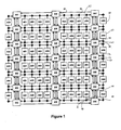
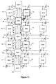
- Figure 1 shows an array architecture in accordance with the present invention.
- the array architecture is generally as described in GB-A-2370380 and GB-A-2370381, with modifications which will be described further herein.
- the array consists of a plurality of array elements 20, arranged in a matrix.
- the example shown in Figure 1 has six rows, each consisting of ten array elements (AE0, AE1, ..., AE9), giving a total of 60 array elements, but a practical embodiment of the invention may for example have over 400 array elements in total.
- Each array element, 20, is connected to a segment of a respective first horizontal bus 32 running from left to right, and to a segment of a respective second horizontal bus 36 running from right to left, by means of respective connectors 50.
- the horizontal bus segments 32, 36 are connected to vertical bus segments 41, 43 running upwards and to vertical bus segments 42, 44 running downwards, at switches 55.
- each switch 55 has an input left-right horizontal bus segment 32, an input right-left horizontal bus segment 36, two input upwards vertical bus segments 41, 43, and two input downwards vertical bus segments 42, 44, plus an output left-right horizontal bus segment 32, an output right-left horizontal bus segment 36, two output upwards vertical bus segments 41, 43, and two output downwards vertical bus segments 42, 44.
- All horizontal bus segments 32, 36 and vertical bus segments 41, 43, 42, 44 are 32 bits wide.
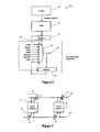
- FIG. 2 shows the structure of one of the switches 55, each of the switches being the same.
- the switch includes a random access memory RAM 61, which is preloaded with data.
- the switch 55 is locally controlled by a controller 60, which contains a counter that counts through the addresses of RAM 61 in a predetermined sequence. This same sequence is repeated indefinitely, and the time taken to complete the sequence once, measured in cycles of the system clock, is referred to as the sequence period.
- the output data from RAM 61 is loaded into a register 62, and the content of the register 62 is used to select the source for each output bus 66 using multiplexer 64.
- the source for the output bus 66 may be any one of the six input buses, namely the input left-right horizontal bus segment LeftIn, the input right-left horizontal bus segment RightIn, the two input upwards vertical bus segments UplIt and Up2In, or the two input downwards vertical bus segments DownlIn and Down2In.
- the value zero can be selected as the source for an output bus, as can the value that was on the output bus during a previous clock cycle, which is loaded into a register 65 under the control of one of the bits in register 62.
- the biggest component of the switch 55 is the RAM 61, although this is still small by the standards of RAMs generally. Therefore, the size of the RAM 61 is dictated to a large extent by the address decoding section of the RAM. Since this is not dependent on the number of buses being switched in the switch 55, the overall size of the device can be reduced by providing two pairs of vertical buses, and one switch in each row, after a group of four columns of array elements, as compared with providing, say, one pair of vertical buses, and one switch in each row, after each group of two columns of array elements.
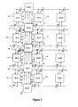
- FIG. 3 shows in more detail how each array element 20 is connected to the segments of the horizontal buses 32, 36 at a connector 50.
- Each such connector 50 includes a multiplexer 51, and a segment of the bus is defined as the portion between two such multiplexers 51.
- Each segment of a left-right horizontal bus 32 is connected to an input of a respective array element 20 by means of a connection 21.
- An output 22 of each array element 20 is connected to a respective segment of a right-left horizontal bus 36 through another multiplexer 51.
- Each multiplexer 51 is under control of circuitry (not shown) within the associated array element 20, which determines whether the multiplexer outputs the data on the input bus segment or the data on the array element output.
- All communication within the array takes place in a predetermined sequence, which lasts for a predetermined number (for example, 1024) of clock cycles (the sequence period that is described above).
- Each switch and each array element contains a counter that counts for the sequence period.
- each switch selects data from one of the eight possible sources onto each of its six output buses.
- array elements load data in from the respective input bus segments via the respective connections 21, and switch data onto the respective output bus segments, using the multiplexers 51.
- Each array element is capable of controlling its associated multiplexer, and loading data from the bus segments to which it is connected at the correct times in sequence, and of performing some useful function on the data.
- the useful function may consist only of storing the data.
- each array element contains a complex microprocessor, the area of which is several times more than that of each switch. This difference in size makes the present invention, which is concerned with overcoming failures in the array elements rather than in the switches, particularly effective.
- FIG. 4 shows the boundary of a circular silicon wafer 60, the individual square dice 61 which are used for making individual devices, and randomly distributed defects 62.
- the array of processing elements incorporates a degree of redundancy. More specifically, one or more spare (redundant) rows of array elements, over and above the number required to implement the intended function or functions of the device, is included in the array. If a defect occurs in one of the processing elements, either during manufacturing or in operation of the device, then the entire row of array elements which includes the defective processing element is not used, and is replaced by a spare row.
- each row of array elements is identical, and all of the functionality of the row that includes the defective processing element can be performed by the spare row.
- the software programs that would otherwise have been loaded into the array elements of Row 2 are loaded into the corresponding array elements of Row 3; the software programs that would otherwise have been loaded into the array elements of Row 3 are loaded into the corresponding array elements of Row 4; and the software programs that would otherwise have been loaded into the array elements of Row 4 are loaded into the corresponding array elements of Row 5.
- the contents of the RAMs in the switches must also be changed, so that the data is transferred to the array element which will now be using it.
- the programs are redistributed in such a way that programs which are run on array elements above the row with the defective array element are run on the same array element, while programs which are run on array elements in or below the row with the defective array element are run on the corresponding array element in the row below their original row.
- the RAMs are reprogrammed so that the routes taken by data move down with the failed row and the rows below it, and stay in the same places in the row above the failed row.
- Data is rerouted according to the rules set out below.
- Routes lying entirely below the failed row are all moved down by one row, in the same way as horizontal routes, as described above.
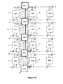
- Routes to the failed row from the row above the failed row that do not use any vertical bus segments form a special case. Specifically, as illustrated in Figure 11, the original route contains no existing vertical bus segments to extend, unlike the example shown in Figure 10. As a result, a new vertical section must be inserted. This could lead to a potential problem, as the vertical bus segment that is required for the new route may have already been allocated to another route during the required time slot.
- Routes starting from the failed row and going down, as shown in Figure 12, are handled in the same way as routes lying entirely below the failed row. For example, a route from array element AE25 to AE35, via bus segment 87, switch SW31, and bus segment 89, is moved to a route from array element AE35 to AE45, via bus segment 95, switch SW41, and bus segment 107.
- Routes coming from the failed.row and going up, where the original route includes at least one vertical bus segment are extended by one vertical bus segment as illustrated in Figure 13.
- a route from array element AE25 to AE15, via bus segment 87, switch SW31, bus segment 83, switch SW21, bus segment 71 and switch SW11 is altered so that it starts at array element AE35, and is routed to SW31 via bus segment 95, switch SE41, and bus segment 91, thereafter continuing as before to AE15.
- FIG 14. A route from the failed row, to the row above, not using any vertical bus segments, is illustrated in Figure 14. This is analogous to the case shown in Figure 11, above. Specifically, a route from array element AE24 to AE14 via bus segment 80, switch SW21 and bus segment 74 is replaced by a route from array element AE34 to AE14 via bus segment 88, switch SW31, bus segment 84, switch SW21 and bus segment 74. Thus, a connection on bus segment 84 (or on the other bus segment 83 that runs from switch SW31 to SW21) must be reserved for that time slot by the original route allocation process, to avoid the possibility of contention. Routes that cross the failed row are shown in Figure 15 (running upwards) and Figure 16 (running downwards). In these cases, the allocations of all the vertical bus segments below the failed row are moved down by one row, and an extra bus segment is allocated in the failed row.
- the information about which rows contain failures may be used to blow laser fuses on the devices under test.
- the process that loads programs onto the array elements and manipulates the data in the RAMs of the switches may use this information at the time the array is configured.
- the method described here may be used to repair failures that occur during operation in the field. In this case, failures in array elements may be detected by running test software on the array elements.
- processor elements include microprocessors.
- the processor elements may simply be able to store data.
- each processor element may itself contain an array of smaller processor.elements.
Claims (7)
- Verfahren zum Zuweisen einer Funktionalität an Prozessorelemente (20) in einer Prozessoranordnung, wobei die Prozessoranordnung zahlreiche Prozessorelemente (20) umfasst, die in einer Anordnung mit Zeilen und Spalten arrangiert sind, und die Prozessorelemente (20) durch Busse (32, 36, 41-44) verbunden sind, die zwischen den Zeilen und Spalten verlaufen, und durch Schalter (55), die sich an den Kreuzungen der Busse (32, 36, 41-44) befinden, und bei Betrieb der Prozessoranordnung Daten während Zeitschlitzen zwischen Prozessorelementen (20) übertragen werden, und zwar über horizontale Busse (32, 36), die zwischen den Zeilen der Prozessorelemente (20) verlaufen, und über vertikale Busse (41 - 44), die zwischen den Spalten der Prozessorelemente (20) verlaufen, und das Verfahren umfasst:das Kennzeichnen einer Zeile als redundante Zeile, der anfänglich keine Funktionalität zugewiesen wird, so dass man für den Fall, dass man ein erstes Prozessorelement als fehlerhaft erkennt, die Funktionalität von der Zeile entfernen kann, die das erste Prozessorelement enthält, und man die Funktionalität statt dessen der redundanten Zeile zuweisen kann; undbeim Zuweisen der Funktionalität an die Prozessorelemente, so dass Daten, die für das Übertragen eingeplant sind, und zwar während eines ersten Zeitschlitzes von einem ersten Prozessorelement in einer ersten Zeile an ein zweites Prozessorelement in einer zweiten Zeile, die sich von der ersten Zeile unterscheidet, und dies über einen der Schalter ohne irgendeinen vertikalen Bus zu benutzen, das Reservieren des Zeitschlitzes für die geplante Datenübertragung auf einem Segment eines vertikalen Busses, den man im Fall der Neuzuweisung von Funktionalität verwendet, nachdem man festgestellt hat, dass entweder das erste Prozessorelement oder das zweite Prozessorelement fehlerhaft ist.
- Verfahren nach Anspruch 1, zudem umfassend:für den Fall, dass sich ein erstes Prozessorelement als fehlerhaft herausstellt, das Zuweisen der Funktionalität, die von der Zeile weggenommen wurde, die das erste Prozessorelement enthält, an eine benachbarte Zeile; und das erneute Zuweisen der Funktionalität von der benachbarten Zeile an eine weitere hierzu benachbarte Zeile, und dies solange, bis der redundanten Zeile Funktionalität zugewiesen ist.
- Verfahren nach Anspruch 1 oder 2, wobei sich die redundante Zeile an einer Kante der Anordnung befindet.
- Prozessoranordnung, umfassend:zahlreiche Prozessorelemente (20), die in einer Anordnung mit Zeilen und Spalten arrangiert sind;Busse (32, 36, 41-44), die zwischen den Zeilen und Spalten verlaufen; undSchalter (55), die sich an den Kreuzungen der Busse (32, 36, 41-44) befinden,wobei:die Prozessorelemente (20) über die Busse (32, 36, 41-44) und die Schalter (55) verbunden sind,die Prozessoranordnung so ausgelegt ist, dass sie Daten während Zeitschlitzen zwischen Prozessorelementen (20) überträgt, und zwar über horizontale Busse (32, 36), die zwischen den Zeilen der Prozessorelemente (20) verlaufen, und über vertikale Busse (41 - 44), die zwischen den Spalten der Prozessorelemente (20) verlaufen,eine Zeile als redundante Zeile gekennzeichnet wird, der anfänglich keine Funktionalität zugewiesen wird, so dass man für den Fall, dass man ein erstes Prozessorelement als fehlerhaft erkennt, die Funktionalität von der Zeile entfernen kann, die das erste Prozessorelement enthält, und man die Funktionalität statt dessen der redundanten Zeile zuweisen kann; undbeim Zuweisen der Funktionalität an die Prozessorelemente, so dass Daten, die für das Übertragen eingeplant sind, und zwar während eines ersten Zeitschlitzes von einem ersten Prozessorelement in einer ersten Zeile an ein zweites Prozessorelement in einer zweiten Zeile, die sich von der ersten Zeile unterscheidet, und dies über einen der Schalter ohne irgendeinen vertikalen Bus zu benutzen, die Prozessoranordnung so beschaffen ist, dass sie den Zeitschlitz für die geplante Datenübertragung auf einem Segment eines vertikalen Busses reserviert, den man im Fall der Neuzuweisung von Funktionalität verwendet, nachdem man festgestellt hat, dass entweder das erste Prozessorelement oder das zweite Prozessorelement fehlerhaft ist.
- Prozessoranordnung nach Anspruch 4,
worin:die Anordnung der Prozessorelemente in jeder Zeile mit der Anordnung der Prozessorelemente in jeder anderen Zeile übereinstimmt,die horizontalen Busse (32, 36) Paare von horizontalen Bussen enthalten, die zwischen den Zeilen der Prozessorelemente (20) verlaufen, und jedes Paar einen ersten horizontalen Bus umfasst, der Daten in einer ersten Richtung befördert, und einen zweiten horizontalen Bus, der Daten in einer zweiten Richtung befördert, die der ersten Richtung entgegengesetzt ist,einige Paare von benachbarten Spalten der Prozessorelemente keine vertikalen Busse (41 - 44) aufweisen, die zwischen ihnen verlaufen, und andere Paare von benachbarten Spalten zwei zwischen ihnen verlaufende Busse (41, 43) aufweisen, die Daten in einer ersten Richtung befördern, und zwei Busse (42, 44), die Daten in einer zweiten Richtung befördern, die der ersten Richtung entgegengesetzt ist, unddie Schalter (55) an den Kreuzungen der horizontalen und der vertikalen Busse angeordnet sind. - Prozessoranordnung nach Anspruch 5, wobei jeder Schalter (55) umfasst:zahlreiche Eingabebusse und zahlreiche Ausgabebusse;eine Speichervorrichtung (61), die an jeder ihrer Adressen Information speichert, die angibt, welche Daten auf jeden Ausgabebus zu schalten sind; undeinen Controller (60), der die Adressen der Speichervorrichtung (61) in einer vorbestimmten Reihenfolge durchzählt.
- Prozessoranordnung nach Anspruch 6, wobei die Speichervorrichtung (61) Information speichert, die angibt, ob die auf jeden der Ausgabebusse zu schaltenden Daten sind:der Datenwert an einem der Eingabebusse;der vorhergehende Datenwert auf diesem Ausgabebus; oderder Wert Null.
Applications Claiming Priority (3)
| Application Number | Priority Date | Filing Date | Title |
|---|---|---|---|
| GB0216880A GB2391083B (en) | 2002-07-19 | 2002-07-19 | Processor array |
| GB0216880 | 2002-07-19 | ||
| PCT/GB2003/002772 WO2004010321A2 (en) | 2002-07-19 | 2003-06-27 | Processor array |
Publications (2)
| Publication Number | Publication Date |
|---|---|
| EP1535192A2 EP1535192A2 (de) | 2005-06-01 |
| EP1535192B1 true EP1535192B1 (de) | 2007-05-09 |
Family
ID=9940825
Family Applications (1)
| Application Number | Title | Priority Date | Filing Date |
|---|---|---|---|
| EP03765145A Expired - Lifetime EP1535192B1 (de) | 2002-07-19 | 2003-06-27 | Gatterprozessor |
Country Status (11)
| Country | Link |
|---|---|
| US (1) | US7549081B2 (de) |
| EP (1) | EP1535192B1 (de) |
| JP (1) | JP4467430B2 (de) |
| CN (1) | CN100416545C (de) |
| AT (1) | ATE362139T1 (de) |
| AU (1) | AU2003250383A1 (de) |
| DE (1) | DE60313781T2 (de) |
| ES (1) | ES2285191T3 (de) |
| GB (2) | GB2391083B (de) |
| TW (1) | TWI314682B (de) |
| WO (1) | WO2004010321A2 (de) |
Families Citing this family (31)
| Publication number | Priority date | Publication date | Assignee | Title |
|---|---|---|---|---|
| GB2370380B (en) | 2000-12-19 | 2003-12-31 | Picochip Designs Ltd | Processor architecture |
| CN1310133C (zh) * | 2004-08-04 | 2007-04-11 | 联合信源数字音视频技术(北京)有限公司 | 一种视频图象象素插值装置 |
| GB2454865B (en) | 2007-11-05 | 2012-06-13 | Picochip Designs Ltd | Power control |
| GB2457310B (en) * | 2008-02-11 | 2012-03-21 | Picochip Designs Ltd | Signal routing in processor arrays |
| GB2457309A (en) | 2008-02-11 | 2009-08-12 | Picochip Designs Ltd | Process allocation in a processor array using a simulated annealing method |
| US20090315909A1 (en) | 2008-05-30 | 2009-12-24 | Advanced Micro Devices, Inc. | Unified Shader Engine Filtering System |
| KR101465771B1 (ko) * | 2008-05-30 | 2014-11-27 | 어드밴스드 마이크로 디바이시즈, 인코포레이티드 | 셰이더 열 리페어를 위한 리던던시 방법 및 장치 |
| GB2466661B (en) * | 2009-01-05 | 2014-11-26 | Intel Corp | Rake receiver |
| GB2470037B (en) | 2009-05-07 | 2013-07-10 | Picochip Designs Ltd | Methods and devices for reducing interference in an uplink |
| GB2470891B (en) | 2009-06-05 | 2013-11-27 | Picochip Designs Ltd | A method and device in a communication network |
| GB2470771B (en) | 2009-06-05 | 2012-07-18 | Picochip Designs Ltd | A method and device in a communication network |
| GB2474071B (en) | 2009-10-05 | 2013-08-07 | Picochip Designs Ltd | Femtocell base station |
| GB2482869B (en) | 2010-08-16 | 2013-11-06 | Picochip Designs Ltd | Femtocell access control |
| US8688957B2 (en) * | 2010-12-21 | 2014-04-01 | Intel Corporation | Mechanism for conflict detection using SIMD |
| GB2489716B (en) | 2011-04-05 | 2015-06-24 | Intel Corp | Multimode base system |
| GB2489919B (en) | 2011-04-05 | 2018-02-14 | Intel Corp | Filter |
| GB2491098B (en) | 2011-05-16 | 2015-05-20 | Intel Corp | Accessing a base station |
| JP2014016894A (ja) * | 2012-07-10 | 2014-01-30 | Renesas Electronics Corp | 並列演算装置、並列演算装置を備えたデータ処理システム、及び、データ処理プログラム |
| US9160617B2 (en) | 2012-09-28 | 2015-10-13 | International Business Machines Corporation | Faulty core recovery mechanisms for a three-dimensional network on a processor array |
| US8990616B2 (en) * | 2012-09-28 | 2015-03-24 | International Business Machines Corporation | Final faulty core recovery mechanisms for a two-dimensional network on a processor array |
| US9411584B2 (en) | 2012-12-29 | 2016-08-09 | Intel Corporation | Methods, apparatus, instructions, and logic to provide vector address conflict detection functionality |
| US9411592B2 (en) | 2012-12-29 | 2016-08-09 | Intel Corporation | Vector address conflict resolution with vector population count functionality |
| US20140244218A1 (en) * | 2013-02-25 | 2014-08-28 | International Business Machines Corporation | Architecture optimization |
| TWI490784B (zh) * | 2013-05-16 | 2015-07-01 | Wistron Neweb Corp | 功能模組管理方法及電子系統 |
| US10552740B2 (en) | 2014-11-10 | 2020-02-04 | International Business Machines Corporation | Fault-tolerant power-driven synthesis |
| CN107547451B (zh) * | 2017-05-31 | 2020-04-03 | 新华三信息技术有限公司 | 一种多路服务器、cpu连接方法及装置 |
| JP6926708B2 (ja) * | 2017-06-14 | 2021-08-25 | 住友電気工業株式会社 | 車載通信システム、スイッチ装置、通信制御方法および通信制御プログラム |
| EP3662474B1 (de) | 2017-07-30 | 2023-02-22 | NeuroBlade Ltd. | Speicherbasierte verteilte prozessorarchitektur |
| US10691632B1 (en) * | 2019-03-14 | 2020-06-23 | DeGirum Corporation | Permutated ring network interconnected computing architecture |
| CN112820202B (zh) * | 2019-10-30 | 2023-03-28 | 海信视像科技股份有限公司 | 一种显示装置及其显示方法 |
| US20230237011A1 (en) * | 2022-01-21 | 2023-07-27 | Nvidia Corporation | Mapping logical and physical processors and logical and physical memory |
Family Cites Families (17)
| Publication number | Priority date | Publication date | Assignee | Title |
|---|---|---|---|---|
| US174318A (en) * | 1876-02-29 | Improvement in safety hoisting apparatus | ||
| US4389715A (en) * | 1980-10-06 | 1983-06-21 | Inmos Corporation | Redundancy scheme for a dynamic RAM |
| JPS58137192A (ja) * | 1981-12-29 | 1983-08-15 | Fujitsu Ltd | 半導体記憶装置 |
| GB2129585B (en) * | 1982-10-29 | 1986-03-05 | Inmos Ltd | Memory system including a faulty rom array |
| EP0190813B1 (de) * | 1985-01-29 | 1991-09-18 | The Secretary of State for Defence in Her Britannic Majesty's Government of the United Kingdom of Great Britain and | Verarbeitungszelle für fehlertolerante Matrixanordnungen |
| GB8612454D0 (en) * | 1986-05-22 | 1986-07-02 | Inmos Ltd | Redundancy scheme for multi-stage apparatus |
| US5253308A (en) * | 1989-06-21 | 1993-10-12 | Amber Engineering, Inc. | Massively parallel digital image data processor using pixel-mapped input/output and relative indexed addressing |
| HU900629D0 (en) | 1990-02-01 | 1990-04-28 | Cellware Mikroelektronikai Kut | Cicuit arrangement for inhomogen operating processors with homogen structure and cellular building |
| US6408402B1 (en) * | 1994-03-22 | 2002-06-18 | Hyperchip Inc. | Efficient direct replacement cell fault tolerant architecture |
| JP3345626B2 (ja) * | 1994-09-29 | 2002-11-18 | 富士通株式会社 | マルチプロセッサシステムにおけるプロセッサ異常対策装置およびマルチプロセッサシステムにおけるプロセッサ異常対策方法 |
| US5795797A (en) * | 1995-08-18 | 1998-08-18 | Teradyne, Inc. | Method of making memory chips using memory tester providing fast repair |
| DE19907567B4 (de) * | 1999-02-22 | 2007-08-09 | Forschungszentrum Jülich GmbH | Verfahren zur mikrobiellen Herstellung von L-Valin |
| GB2348976A (en) * | 1999-04-09 | 2000-10-18 | Pixelfusion Ltd | Single instruction multiple data array |
| EP1181648A1 (de) * | 1999-04-09 | 2002-02-27 | Clearspeed Technology Limited | Paralleldatenverarbeitungsvorrichtung |
| FR2795839B1 (fr) * | 1999-07-02 | 2001-09-07 | Commissariat Energie Atomique | Procede de reconfiguration applicable a un reseau d'elements fonctionnels identiques |
| US6681341B1 (en) * | 1999-11-03 | 2004-01-20 | Cisco Technology, Inc. | Processor isolation method for integrated multi-processor systems |
| GB2370380B (en) * | 2000-12-19 | 2003-12-31 | Picochip Designs Ltd | Processor architecture |
-
2002
- 2002-07-19 GB GB0216880A patent/GB2391083B/en not_active Expired - Fee Related
- 2002-07-19 GB GB0520346A patent/GB2417586B/en not_active Expired - Fee Related
-
2003
- 2003-06-27 AT AT03765145T patent/ATE362139T1/de not_active IP Right Cessation
- 2003-06-27 ES ES03765145T patent/ES2285191T3/es not_active Expired - Lifetime
- 2003-06-27 EP EP03765145A patent/EP1535192B1/de not_active Expired - Lifetime
- 2003-06-27 DE DE60313781T patent/DE60313781T2/de not_active Expired - Lifetime
- 2003-06-27 AU AU2003250383A patent/AU2003250383A1/en not_active Abandoned
- 2003-06-27 WO PCT/GB2003/002772 patent/WO2004010321A2/en active IP Right Grant
- 2003-06-27 US US10/521,889 patent/US7549081B2/en active Active
- 2003-06-27 CN CNB038198207A patent/CN100416545C/zh not_active Expired - Lifetime
- 2003-06-27 JP JP2004522285A patent/JP4467430B2/ja not_active Expired - Fee Related
- 2003-07-10 TW TW092118854A patent/TWI314682B/zh not_active IP Right Cessation
Also Published As
| Publication number | Publication date |
|---|---|
| US20050257105A1 (en) | 2005-11-17 |
| WO2004010321A3 (en) | 2005-03-31 |
| CN1675633A (zh) | 2005-09-28 |
| WO2004010321A2 (en) | 2004-01-29 |
| TW200417853A (en) | 2004-09-16 |
| GB2417586B (en) | 2007-03-28 |
| AU2003250383A1 (en) | 2004-02-09 |
| JP4467430B2 (ja) | 2010-05-26 |
| ES2285191T3 (es) | 2007-11-16 |
| GB2391083B (en) | 2006-03-01 |
| DE60313781D1 (de) | 2007-06-21 |
| CN100416545C (zh) | 2008-09-03 |
| DE60313781T2 (de) | 2008-01-24 |
| GB2391083A (en) | 2004-01-28 |
| GB0520346D0 (en) | 2005-11-16 |
| JP2005534091A (ja) | 2005-11-10 |
| US7549081B2 (en) | 2009-06-16 |
| TWI314682B (en) | 2009-09-11 |
| EP1535192A2 (de) | 2005-06-01 |
| GB2417586A (en) | 2006-03-01 |
| GB0216880D0 (en) | 2002-08-28 |
| ATE362139T1 (de) | 2007-06-15 |
Similar Documents
| Publication | Publication Date | Title |
|---|---|---|
| EP1535192B1 (de) | Gatterprozessor | |
| US9804221B2 (en) | Configurable vertical integration | |
| US6337578B2 (en) | Redundancy circuitry for programmable logic devices with interleaved input circuits | |
| EP0425807A1 (de) | Umkehrkreuzungsschalter mit verteilter Steuerung | |
| US7584390B2 (en) | Method and system for alternating between programs for execution by cells of an integrated circuit | |
| EP1170666A2 (de) | Online fehlertoleranter Betrieb durch inkrementelle Rekonfigurierung eines feldprogrammierbaren Gatterfeldes | |
| US4415973A (en) | Array processor with stand-by for replacing failed section | |
| JPS58111200A (ja) | デ−タ処理システム | |
| JPH10143465A (ja) | データ転送システム | |
| JPH11143729A (ja) | フォールトトレラントコンピュータ | |
| JP3215919B2 (ja) | メモリ管理 | |
| JP2509343B2 (ja) | 半導体メモリ装置 | |
| US20220113350A1 (en) | Segmented row repair for programmable logic devices | |
| Campbell et al. | Hierarchical fault tolerance for 3D microelectronics | |
| Kwiat et al. | Efficient hardware fault tolerance using field-programmable gate arrays | |
| JP2727856B2 (ja) | 大規模メモリ構成方法 | |
| Negrini et al. | Fault-tolerance techniques in arrays for image processing | |
| JPH04132094A (ja) | ダイナミックramの制御回路 | |
| JPH03129856A (ja) | ウエハ・スケール集積回路の冗長方法 | |
| JPS60138656A (ja) | 記憶装置の符号変換方式 | |
| JPS59178548A (ja) | 多重化システム制御方式 | |
| JPH0553848A (ja) | フオールトトレラントシステム | |
| JPS6168659A (ja) | Rom自動切換回路 |
Legal Events
| Date | Code | Title | Description |
|---|---|---|---|
| PUAI | Public reference made under article 153(3) epc to a published international application that has entered the european phase |
Free format text: ORIGINAL CODE: 0009012 |
|
| 17P | Request for examination filed |
Effective date: 20050221 |
|
| AK | Designated contracting states |
Kind code of ref document: A2 Designated state(s): AT BE BG CH CY CZ DE DK EE ES FI FR GB GR HU IE IT LI LU MC NL PT RO SE SI SK TR |
|
| AX | Request for extension of the european patent |
Extension state: AL LT LV MK |
|
| DAX | Request for extension of the european patent (deleted) | ||
| GRAP | Despatch of communication of intention to grant a patent |
Free format text: ORIGINAL CODE: EPIDOSNIGR1 |
|
| GRAS | Grant fee paid |
Free format text: ORIGINAL CODE: EPIDOSNIGR3 |
|
| GRAA | (expected) grant |
Free format text: ORIGINAL CODE: 0009210 |
|
| AK | Designated contracting states |
Kind code of ref document: B1 Designated state(s): AT BE BG CH CY CZ DE DK EE ES FI FR GR HU IE IT LI LU MC NL PT RO SE SI SK TR |
|
| PG25 | Lapsed in a contracting state [announced via postgrant information from national office to epo] |
Ref country code: CH Free format text: LAPSE BECAUSE OF FAILURE TO SUBMIT A TRANSLATION OF THE DESCRIPTION OR TO PAY THE FEE WITHIN THE PRESCRIBED TIME-LIMIT Effective date: 20070509 Ref country code: LI Free format text: LAPSE BECAUSE OF FAILURE TO SUBMIT A TRANSLATION OF THE DESCRIPTION OR TO PAY THE FEE WITHIN THE PRESCRIBED TIME-LIMIT Effective date: 20070509 |
|
| RBV | Designated contracting states (corrected) |
Designated state(s): AT BE BG CH CY CZ DE DK EE ES FI FR GR HU IE IT LI LU MC NL PT RO SE SI SK TR |
|
| REG | Reference to a national code |
Ref country code: CH Ref legal event code: EP |
|
| REG | Reference to a national code |
Ref country code: IE Ref legal event code: FG4D |
|
| REF | Corresponds to: |
Ref document number: 60313781 Country of ref document: DE Date of ref document: 20070621 Kind code of ref document: P |
|
| REG | Reference to a national code |
Ref country code: SE Ref legal event code: TRGR |
|
| ET | Fr: translation filed | ||
| NLV1 | Nl: lapsed or annulled due to failure to fulfill the requirements of art. 29p and 29m of the patents act | ||
| REG | Reference to a national code |
Ref country code: CH Ref legal event code: PL |
|
| REG | Reference to a national code |
Ref country code: ES Ref legal event code: FG2A Ref document number: 2285191 Country of ref document: ES Kind code of ref document: T3 |
|
| PG25 | Lapsed in a contracting state [announced via postgrant information from national office to epo] |
Ref country code: AT Free format text: LAPSE BECAUSE OF FAILURE TO SUBMIT A TRANSLATION OF THE DESCRIPTION OR TO PAY THE FEE WITHIN THE PRESCRIBED TIME-LIMIT Effective date: 20070509 |
|
| PG25 | Lapsed in a contracting state [announced via postgrant information from national office to epo] |
Ref country code: BE Free format text: LAPSE BECAUSE OF FAILURE TO SUBMIT A TRANSLATION OF THE DESCRIPTION OR TO PAY THE FEE WITHIN THE PRESCRIBED TIME-LIMIT Effective date: 20070509 |
|
| PG25 | Lapsed in a contracting state [announced via postgrant information from national office to epo] |
Ref country code: MC Free format text: LAPSE BECAUSE OF NON-PAYMENT OF DUE FEES Effective date: 20070630 Ref country code: PT Free format text: LAPSE BECAUSE OF FAILURE TO SUBMIT A TRANSLATION OF THE DESCRIPTION OR TO PAY THE FEE WITHIN THE PRESCRIBED TIME-LIMIT Effective date: 20071009 Ref country code: SI Free format text: LAPSE BECAUSE OF FAILURE TO SUBMIT A TRANSLATION OF THE DESCRIPTION OR TO PAY THE FEE WITHIN THE PRESCRIBED TIME-LIMIT Effective date: 20070509 Ref country code: BG Free format text: LAPSE BECAUSE OF FAILURE TO SUBMIT A TRANSLATION OF THE DESCRIPTION OR TO PAY THE FEE WITHIN THE PRESCRIBED TIME-LIMIT Effective date: 20070809 Ref country code: CZ Free format text: LAPSE BECAUSE OF FAILURE TO SUBMIT A TRANSLATION OF THE DESCRIPTION OR TO PAY THE FEE WITHIN THE PRESCRIBED TIME-LIMIT Effective date: 20070509 Ref country code: DK Free format text: LAPSE BECAUSE OF FAILURE TO SUBMIT A TRANSLATION OF THE DESCRIPTION OR TO PAY THE FEE WITHIN THE PRESCRIBED TIME-LIMIT Effective date: 20070509 Ref country code: NL Free format text: LAPSE BECAUSE OF FAILURE TO SUBMIT A TRANSLATION OF THE DESCRIPTION OR TO PAY THE FEE WITHIN THE PRESCRIBED TIME-LIMIT Effective date: 20070509 |
|
| PG25 | Lapsed in a contracting state [announced via postgrant information from national office to epo] |
Ref country code: SK Free format text: LAPSE BECAUSE OF FAILURE TO SUBMIT A TRANSLATION OF THE DESCRIPTION OR TO PAY THE FEE WITHIN THE PRESCRIBED TIME-LIMIT Effective date: 20070509 |
|
| PLBE | No opposition filed within time limit |
Free format text: ORIGINAL CODE: 0009261 |
|
| STAA | Information on the status of an ep patent application or granted ep patent |
Free format text: STATUS: NO OPPOSITION FILED WITHIN TIME LIMIT |
|
| 26N | No opposition filed |
Effective date: 20080212 |
|
| PG25 | Lapsed in a contracting state [announced via postgrant information from national office to epo] |
Ref country code: GR Free format text: LAPSE BECAUSE OF FAILURE TO SUBMIT A TRANSLATION OF THE DESCRIPTION OR TO PAY THE FEE WITHIN THE PRESCRIBED TIME-LIMIT Effective date: 20070810 |
|
| PG25 | Lapsed in a contracting state [announced via postgrant information from national office to epo] |
Ref country code: RO Free format text: LAPSE BECAUSE OF FAILURE TO SUBMIT A TRANSLATION OF THE DESCRIPTION OR TO PAY THE FEE WITHIN THE PRESCRIBED TIME-LIMIT Effective date: 20070509 Ref country code: IE Free format text: LAPSE BECAUSE OF NON-PAYMENT OF DUE FEES Effective date: 20070627 |
|
| PG25 | Lapsed in a contracting state [announced via postgrant information from national office to epo] |
Ref country code: EE Free format text: LAPSE BECAUSE OF FAILURE TO SUBMIT A TRANSLATION OF THE DESCRIPTION OR TO PAY THE FEE WITHIN THE PRESCRIBED TIME-LIMIT Effective date: 20070509 |
|
| PG25 | Lapsed in a contracting state [announced via postgrant information from national office to epo] |
Ref country code: CY Free format text: LAPSE BECAUSE OF FAILURE TO SUBMIT A TRANSLATION OF THE DESCRIPTION OR TO PAY THE FEE WITHIN THE PRESCRIBED TIME-LIMIT Effective date: 20070509 |
|
| PG25 | Lapsed in a contracting state [announced via postgrant information from national office to epo] |
Ref country code: LU Free format text: LAPSE BECAUSE OF NON-PAYMENT OF DUE FEES Effective date: 20070627 |
|
| PG25 | Lapsed in a contracting state [announced via postgrant information from national office to epo] |
Ref country code: HU Free format text: LAPSE BECAUSE OF FAILURE TO SUBMIT A TRANSLATION OF THE DESCRIPTION OR TO PAY THE FEE WITHIN THE PRESCRIBED TIME-LIMIT Effective date: 20071110 Ref country code: TR Free format text: LAPSE BECAUSE OF FAILURE TO SUBMIT A TRANSLATION OF THE DESCRIPTION OR TO PAY THE FEE WITHIN THE PRESCRIBED TIME-LIMIT Effective date: 20070509 |
|
| REG | Reference to a national code |
Ref country code: DE Ref legal event code: R082 Ref document number: 60313781 Country of ref document: DE Representative=s name: UEXKUELL & STOLBERG, DE |
|
| REG | Reference to a national code |
Ref country code: DE Ref legal event code: R082 Ref document number: 60313781 Country of ref document: DE Representative=s name: UEXKUELL & STOLBERG, DE Effective date: 20140616 Ref country code: DE Ref legal event code: R081 Ref document number: 60313781 Country of ref document: DE Owner name: INTEL CORPORATION, SANTA CLARA, US Free format text: FORMER OWNER: PICOCHIP DESIGNS LTD., BATH, GB Effective date: 20140616 Ref country code: DE Ref legal event code: R082 Ref document number: 60313781 Country of ref document: DE Representative=s name: UEXKUELL & STOLBERG PARTNERSCHAFT VON PATENT- , DE Effective date: 20140616 |
|
| PGFP | Annual fee paid to national office [announced via postgrant information from national office to epo] |
Ref country code: IT Payment date: 20140617 Year of fee payment: 12 Ref country code: FI Payment date: 20140610 Year of fee payment: 12 Ref country code: ES Payment date: 20140528 Year of fee payment: 12 |
|
| REG | Reference to a national code |
Ref country code: FR Ref legal event code: CD Owner name: INTEL CORPORATION, US Effective date: 20141008 Ref country code: FR Ref legal event code: TP Owner name: INTEL CORPORATION, US Effective date: 20141008 |
|
| PGFP | Annual fee paid to national office [announced via postgrant information from national office to epo] |
Ref country code: FR Payment date: 20140609 Year of fee payment: 12 |
|
| REG | Reference to a national code |
Ref country code: ES Ref legal event code: PC2A Owner name: INTEL CORPORATION Effective date: 20150130 |
|
| PG25 | Lapsed in a contracting state [announced via postgrant information from national office to epo] |
Ref country code: IT Free format text: LAPSE BECAUSE OF NON-PAYMENT OF DUE FEES Effective date: 20150627 Ref country code: FI Free format text: LAPSE BECAUSE OF NON-PAYMENT OF DUE FEES Effective date: 20150627 |
|
| REG | Reference to a national code |
Ref country code: FR Ref legal event code: ST Effective date: 20160229 |
|
| PG25 | Lapsed in a contracting state [announced via postgrant information from national office to epo] |
Ref country code: FR Free format text: LAPSE BECAUSE OF NON-PAYMENT OF DUE FEES Effective date: 20150630 |
|
| REG | Reference to a national code |
Ref country code: ES Ref legal event code: FD2A Effective date: 20160727 |
|
| PG25 | Lapsed in a contracting state [announced via postgrant information from national office to epo] |
Ref country code: ES Free format text: LAPSE BECAUSE OF NON-PAYMENT OF DUE FEES Effective date: 20150628 |
|
| PGFP | Annual fee paid to national office [announced via postgrant information from national office to epo] |
Ref country code: SE Payment date: 20170613 Year of fee payment: 15 |
|
| REG | Reference to a national code |
Ref country code: SE Ref legal event code: EUG |
|
| PG25 | Lapsed in a contracting state [announced via postgrant information from national office to epo] |
Ref country code: SE Free format text: LAPSE BECAUSE OF NON-PAYMENT OF DUE FEES Effective date: 20180628 |
|
| REG | Reference to a national code |
Ref country code: DE Ref legal event code: R082 Ref document number: 60313781 Country of ref document: DE Representative=s name: UEXKUELL & STOLBERG PARTNERSCHAFT VON PATENT- , DE Ref country code: DE Ref legal event code: R081 Ref document number: 60313781 Country of ref document: DE Owner name: APPLE INC., CUPERTINO, US Free format text: FORMER OWNER: INTEL CORPORATION, SANTA CLARA, CALIF., US Ref country code: DE Ref legal event code: R082 Ref document number: 60313781 Country of ref document: DE Representative=s name: BARDEHLE PAGENBERG PARTNERSCHAFT MBB PATENTANW, DE |
|
| REG | Reference to a national code |
Ref country code: DE Ref legal event code: R082 Ref document number: 60313781 Country of ref document: DE Representative=s name: BARDEHLE PAGENBERG PARTNERSCHAFT MBB PATENTANW, DE |
|
| PGFP | Annual fee paid to national office [announced via postgrant information from national office to epo] |
Ref country code: DE Payment date: 20220505 Year of fee payment: 20 |
|
| REG | Reference to a national code |
Ref country code: DE Ref legal event code: R071 Ref document number: 60313781 Country of ref document: DE |