EP1533895A2 - Oberflächenwellenfilter und Funkgerät mit einem derartigen Filter - Google Patents
Oberflächenwellenfilter und Funkgerät mit einem derartigen Filter Download PDFInfo
- Publication number
- EP1533895A2 EP1533895A2 EP04257181A EP04257181A EP1533895A2 EP 1533895 A2 EP1533895 A2 EP 1533895A2 EP 04257181 A EP04257181 A EP 04257181A EP 04257181 A EP04257181 A EP 04257181A EP 1533895 A2 EP1533895 A2 EP 1533895A2
- Authority
- EP
- European Patent Office
- Prior art keywords
- idt
- shield electrode
- filter
- present
- saw filter
- Prior art date
- Legal status (The legal status is an assumption and is not a legal conclusion. Google has not performed a legal analysis and makes no representation as to the accuracy of the status listed.)
- Withdrawn
Links
- 238000010897 surface acoustic wave method Methods 0.000 title claims abstract description 57
- 239000000758 substrate Substances 0.000 claims abstract description 24
- 230000008878 coupling Effects 0.000 claims abstract description 6
- 238000010168 coupling process Methods 0.000 claims abstract description 6
- 238000005859 coupling reaction Methods 0.000 claims abstract description 6
- 230000000052 comparative effect Effects 0.000 description 10
- 230000005540 biological transmission Effects 0.000 description 4
- 230000005236 sound signal Effects 0.000 description 3
- 230000007257 malfunction Effects 0.000 description 2
- 239000000463 material Substances 0.000 description 2
- WSMQKESQZFQMFW-UHFFFAOYSA-N 5-methyl-pyrazole-3-carboxylic acid Chemical compound CC1=CC(C(O)=O)=NN1 WSMQKESQZFQMFW-UHFFFAOYSA-N 0.000 description 1
- 229910000881 Cu alloy Inorganic materials 0.000 description 1
- XAGFODPZIPBFFR-UHFFFAOYSA-N aluminium Chemical compound [Al] XAGFODPZIPBFFR-UHFFFAOYSA-N 0.000 description 1
- 229910052782 aluminium Inorganic materials 0.000 description 1
- WPPDFTBPZNZZRP-UHFFFAOYSA-N aluminum copper Chemical compound [Al].[Cu] WPPDFTBPZNZZRP-UHFFFAOYSA-N 0.000 description 1
- 238000007796 conventional method Methods 0.000 description 1
- 230000003247 decreasing effect Effects 0.000 description 1
- 238000010586 diagram Methods 0.000 description 1
- 230000005284 excitation Effects 0.000 description 1
- GQYHUHYESMUTHG-UHFFFAOYSA-N lithium niobate Chemical compound [Li+].[O-][Nb](=O)=O GQYHUHYESMUTHG-UHFFFAOYSA-N 0.000 description 1
- 238000000034 method Methods 0.000 description 1
- 238000012986 modification Methods 0.000 description 1
- 230000004048 modification Effects 0.000 description 1
- 230000010355 oscillation Effects 0.000 description 1
Images


Classifications
-
- H—ELECTRICITY
- H03—ELECTRONIC CIRCUITRY
- H03H—IMPEDANCE NETWORKS, e.g. RESONANT CIRCUITS; RESONATORS
- H03H9/00—Networks comprising electromechanical or electro-acoustic elements; Electromechanical resonators
- H03H9/46—Filters
- H03H9/64—Filters using surface acoustic waves
-
- H—ELECTRICITY
- H03—ELECTRONIC CIRCUITRY
- H03H—IMPEDANCE NETWORKS, e.g. RESONANT CIRCUITS; RESONATORS
- H03H9/00—Networks comprising electromechanical or electro-acoustic elements; Electromechanical resonators
- H03H9/0023—Networks for transforming balanced signals into unbalanced signals and vice versa, e.g. baluns, or networks having balanced input and output
- H03H9/0028—Networks for transforming balanced signals into unbalanced signals and vice versa, e.g. baluns, or networks having balanced input and output using surface acoustic wave devices
- H03H9/0033—Networks for transforming balanced signals into unbalanced signals and vice versa, e.g. baluns, or networks having balanced input and output using surface acoustic wave devices having one acoustic track only
- H03H9/0038—Networks for transforming balanced signals into unbalanced signals and vice versa, e.g. baluns, or networks having balanced input and output using surface acoustic wave devices having one acoustic track only the balanced terminals being on the same side of the track
-
- H—ELECTRICITY
- H03—ELECTRONIC CIRCUITRY
- H03H—IMPEDANCE NETWORKS, e.g. RESONANT CIRCUITS; RESONATORS
- H03H9/00—Networks comprising electromechanical or electro-acoustic elements; Electromechanical resonators
- H03H9/0023—Networks for transforming balanced signals into unbalanced signals and vice versa, e.g. baluns, or networks having balanced input and output
- H03H9/0028—Networks for transforming balanced signals into unbalanced signals and vice versa, e.g. baluns, or networks having balanced input and output using surface acoustic wave devices
- H03H9/0033—Networks for transforming balanced signals into unbalanced signals and vice versa, e.g. baluns, or networks having balanced input and output using surface acoustic wave devices having one acoustic track only
- H03H9/0042—Networks for transforming balanced signals into unbalanced signals and vice versa, e.g. baluns, or networks having balanced input and output using surface acoustic wave devices having one acoustic track only the balanced terminals being on opposite sides of the track
-
- H—ELECTRICITY
- H03—ELECTRONIC CIRCUITRY
- H03H—IMPEDANCE NETWORKS, e.g. RESONANT CIRCUITS; RESONATORS
- H03H9/00—Networks comprising electromechanical or electro-acoustic elements; Electromechanical resonators
- H03H9/0023—Networks for transforming balanced signals into unbalanced signals and vice versa, e.g. baluns, or networks having balanced input and output
- H03H9/0028—Networks for transforming balanced signals into unbalanced signals and vice versa, e.g. baluns, or networks having balanced input and output using surface acoustic wave devices
- H03H9/0047—Networks for transforming balanced signals into unbalanced signals and vice versa, e.g. baluns, or networks having balanced input and output using surface acoustic wave devices having two acoustic tracks
- H03H9/0052—Networks for transforming balanced signals into unbalanced signals and vice versa, e.g. baluns, or networks having balanced input and output using surface acoustic wave devices having two acoustic tracks being electrically cascaded
- H03H9/0057—Networks for transforming balanced signals into unbalanced signals and vice versa, e.g. baluns, or networks having balanced input and output using surface acoustic wave devices having two acoustic tracks being electrically cascaded the balanced terminals being on the same side of the tracks
-
- H—ELECTRICITY
- H03—ELECTRONIC CIRCUITRY
- H03H—IMPEDANCE NETWORKS, e.g. RESONANT CIRCUITS; RESONATORS
- H03H9/00—Networks comprising electromechanical or electro-acoustic elements; Electromechanical resonators
- H03H9/0023—Networks for transforming balanced signals into unbalanced signals and vice versa, e.g. baluns, or networks having balanced input and output
- H03H9/0028—Networks for transforming balanced signals into unbalanced signals and vice versa, e.g. baluns, or networks having balanced input and output using surface acoustic wave devices
- H03H9/0047—Networks for transforming balanced signals into unbalanced signals and vice versa, e.g. baluns, or networks having balanced input and output using surface acoustic wave devices having two acoustic tracks
- H03H9/0052—Networks for transforming balanced signals into unbalanced signals and vice versa, e.g. baluns, or networks having balanced input and output using surface acoustic wave devices having two acoustic tracks being electrically cascaded
- H03H9/0061—Networks for transforming balanced signals into unbalanced signals and vice versa, e.g. baluns, or networks having balanced input and output using surface acoustic wave devices having two acoustic tracks being electrically cascaded the balanced terminals being on opposite sides of the tracks
-
- H—ELECTRICITY
- H03—ELECTRONIC CIRCUITRY
- H03H—IMPEDANCE NETWORKS, e.g. RESONANT CIRCUITS; RESONATORS
- H03H9/00—Networks comprising electromechanical or electro-acoustic elements; Electromechanical resonators
- H03H9/0023—Networks for transforming balanced signals into unbalanced signals and vice versa, e.g. baluns, or networks having balanced input and output
- H03H9/0028—Networks for transforming balanced signals into unbalanced signals and vice versa, e.g. baluns, or networks having balanced input and output using surface acoustic wave devices
- H03H9/0047—Networks for transforming balanced signals into unbalanced signals and vice versa, e.g. baluns, or networks having balanced input and output using surface acoustic wave devices having two acoustic tracks
- H03H9/0066—Networks for transforming balanced signals into unbalanced signals and vice versa, e.g. baluns, or networks having balanced input and output using surface acoustic wave devices having two acoustic tracks being electrically parallel
- H03H9/0071—Networks for transforming balanced signals into unbalanced signals and vice versa, e.g. baluns, or networks having balanced input and output using surface acoustic wave devices having two acoustic tracks being electrically parallel the balanced terminals being on the same side of the tracks
-
- H—ELECTRICITY
- H03—ELECTRONIC CIRCUITRY
- H03H—IMPEDANCE NETWORKS, e.g. RESONANT CIRCUITS; RESONATORS
- H03H9/00—Networks comprising electromechanical or electro-acoustic elements; Electromechanical resonators
- H03H9/02—Details
- H03H9/02535—Details of surface acoustic wave devices
- H03H9/02818—Means for compensation or elimination of undesirable effects
- H03H9/02874—Means for compensation or elimination of undesirable effects of direct coupling between input and output transducers
-
- H—ELECTRICITY
- H03—ELECTRONIC CIRCUITRY
- H03H—IMPEDANCE NETWORKS, e.g. RESONANT CIRCUITS; RESONATORS
- H03H9/00—Networks comprising electromechanical or electro-acoustic elements; Electromechanical resonators
- H03H9/02—Details
- H03H9/02535—Details of surface acoustic wave devices
- H03H9/02818—Means for compensation or elimination of undesirable effects
- H03H9/02913—Measures for shielding against electromagnetic fields
-
- H—ELECTRICITY
- H03—ELECTRONIC CIRCUITRY
- H03H—IMPEDANCE NETWORKS, e.g. RESONANT CIRCUITS; RESONATORS
- H03H9/00—Networks comprising electromechanical or electro-acoustic elements; Electromechanical resonators
- H03H9/02—Details
- H03H9/125—Driving means, e.g. electrodes, coils
- H03H9/145—Driving means, e.g. electrodes, coils for networks using surface acoustic waves
Definitions
- This invention generally relates to a surface acoustic wave (hereinafter referred to as SAW) device that employs a piezoelectric material, and more particularly, to a SAW device having multiple interdigital transducers (hereinafter referred to as IDT) that are provided on a piezoelectric substrate, and to wireless devices that employ the same.
- SAW surface acoustic wave
- IDT interdigital transducers
- the SAW filters are widely used for high-frequency circuits on wireless devices as filters.
- the wireless devices are represented by mobile telephones or the like.
- integrated circuits (ICs) that perform a balanced input and output operation have been employed for the high-frequency circuits of the wireless devices.
- the SAW filter is also required to perform the balanced input and output operation.
- Document 1 Japanese Patent Application Publication No. 6-204781 (hereinafter referred to as Document 1) discloses a method of using electrodes as input and output terminals. One electrode that faces the IDT on the input side is used for an input terminal, and the other electrode that faces the IDT on the output side is used for an output terminal.
- Japanese Patent Application Publication No. 11-97966 hereinafter referred to as Document 2 discloses that the IDTs are divided into two groups, that is, input group and output group. The balanced operation is realized by operating those two groups that are 180° out of phase.
- the present invention intends to reduce the stray capacitance between the input-side IDT and the output-side IDT and improve the symmetry between the balanced signals.
- a surface acoustic wave (SAW) filter includes, a piezoelectric substrate, a first interdigital transducer (IDT) for input and a second IDT for output that are provided on the piezoelectric substrate, the first IDT and the second IDT being arranged in a propagation direction, and a shield electrode arranged between the first IDT and the second IDT and/or between interconnection lines that connect the first IDT and the second IDT, at least one of the first IDT and the second IDT being of a longitudinal coupling multi-mode type having a balanced operation.
- IDT interdigital transducer
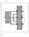
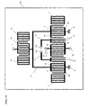
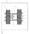
- Fig. 1 is a plan view of a SAW filter of a longitudinal coupling multi-mode type in accordance with a first embodiment of the present invention.
- the SAW filter has a unique shield electrode 12, which will be described after basic components of the first embodiment.
- This SAW filter includes a piezoelectric substrate 100 and three IDTs 4, 5, and 6.
- the piezoelectric substrate 100 is made of lithium tantalate or lithium niobate.
- the three IDTs 4, 5, and 6 are adjacently arranged in a propagation direction on the piezoelectric substrate 100.
- the IDTs 4, 5, and 6 are schematically illustrated in Fig. 1. In fact, the IDT 4 is arranged at the center, and the IDTs 5 and 6 are arranged on both sides of the IDT 4.
- Each of the IDTs 4, 5, and 6 is composed of a pair of comb-like electrodes.
- Each comb-like electrode is composed of a bus bar and electrode fingers that extend from the bus bar.
- the bus bar serves as an interconnection line that connects the electrode fingers together.
- the pair of comb-like electrodes of the IDT 4 includes bus bars 4a and 4b and the electrode fingers that extend from the bus bars 4a and 4b.
- the electrode fingers extending from the bus bar 4a and those extending from the bus bar 4b are alternately overlapped or interleaved, and overlapping parts of the adjacent electrode fingers are involved in excitation of the SAW.
- a pair of comb-like electrodes of the IDT 5 includes bus bars 5a and 5b and the electrode fingers that extend from the bus bars 5a and 5b.
- a pair of comb-like electrodes of the IDT 6 includes bus bars 6a and 6b and the electrode fingers that extend from the bus bars 6a and 6b.
- the bus bar 5a of the IDT 5 and the bus bar 6a of the IDT 6 are connected to a signal line 15, and the bus bar 5b of the IDT 5 and the bus bar 6b of the IDT 6 are connected to a ground 8.
- the bus bars 4a and 4b of the IDT 4 are connected to balanced signal terminals 2a and 2b respectively. Signals that appear on the balanced signal terminals 2a and 2b are balanced signals, that is, the signals having the 180° phase difference.
- a reflector 3 is arranged adjacent to the IDT 5
- a reflector 7 is arranged adjacent to the IDT 6.
- the IDT 10 is composed of a pair of comb-like electrodes. One of the comb-like electrodes is connected to a signal terminal 1, and the other is connected to a signal line 15.
- the signal line 15 connects the IDT 10, the IDT 5, and the IDT 6.
- the signal terminal 1 serves as an input terminal.
- the balanced signal terminals 2a and 2b serve as output terminals. In contrast, the signal terminal 1 may serve as an output terminal.
- the balanced signal terminals 2a and 2b may serve as input terminals.
- the shield electrode 12 is arranged between the bus bar 4a, the balanced signal terminal 2a, a signal line 4c and the signal line 15. Both edges of the shield electrode 12 are respectively arranged between the bus bar 4a and the bus bar 5a, and between the bus bar 4a and the bus bar 6a.
- the shield electrode 12 is also connected to the earth potential 13.
- the shield electrode 12 is arranged between the input IDTs 5 and 6 and the output IDT 4, and between the signal lines 4c and 15.
- the signal line 4c is connected to the IDT 4, and the signal line 15 is connected to the IDTs 5 and 6.
- the shield electrode 12 operates in order to reduce affects on the stray capacitance between input and output.
- Fig. 2 shows an example of the stray capacitance.
- Fig. 2 shows a configuration obtained by omitting the shield electrode 12 and the earth potential 13 from Fig. 1.
- this configuration is referred to as a comparative example.
- a stray capacitance C appears between the adjacent bus bars 4a and 5a, and between the adjacent bus bars 4a and 6a.
- the input voltage passes through the signal line 15 and excites the IDTs 5 and 6.
- part of the current which is leaked current, flows through the stray capacitance C to the bus bar 4a from the bus bars 5a and 6a.
- stray capacitance there exist other stray capacitances.
- stray capacitances there exist small stray capacitances, as compared to the above-mentioned stray capacitance, between the signal line 15 and the bus bar 4a, between the signal line 15 and the signal line 4c, and between the signal line 15 and the balanced signal terminal 2a.
- a stray capacitance also appears between the electrode fingers extending from the bus bar 5a and between those extending from the bus bar 6a, although they are relatively small.
- the shield electrode 12 functions to reduce the affects caused by the above-mentioned stray capacitance C and the other stray capacitances that appear between the signal line 15 and the bus bar 4a, between the signal line 15 and the signal line 4c, and between the signal line 15 and the balanced signal terminal 2a.
- the current leaked from the bus bars 5a and 6a flows to the edges of the shield electrode 12, which are respectively provided between the bus bars 4a and 5a, and between the bus bars 4a and 6a, and then flows out of the earth potential 13 through the shield electrode 12. Therefore, the above-mentioned current leaked from the bus bars 5a and 6a does not flow into the bus bar 4a of the IDT 4.
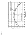
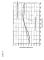
- Figs. 3 and 4 a description will be given that the balanced operation in accordance with the first embodiment of the present invention has a more excellent symmetry than the comparative example.
- the symmetry of the balanced operation may be judged whether is good or bad by examining the symmetries of amplitude and phase.
- Fig. 3 is a graph showing the amplitude symmetries of the balanced output in accordance with the first embodiment of the present invention and the comparative example.
- Fig. 4 is a graph showing phase symmetries in accordance with the first embodiment of the present invention and the comparative example.
- the horizontal axes in Figs. 3 and 4 denote frequency (MHz).
- Figs. 3 denotes frequency symmetry (dB) and the vertical axis in Fig. 4 denotes phase symmetry (degree). On each axis, 0.0 defines the perfect symmetry. As shown in Figs. 3 and 4, it has been found that both the frequency symmetry and phase symmetry are considerably improved.
- the shield electrode 12 is connected to the earth potential 13.
- the earth potential 13 is not connected to the ground potential 8 to which the IDTs 5 and 6 are connected. That is, the potential connected to the shield electrode 12, which is the earth potential, is in a circuitry different from the circuitry in which the ground potential of the IDTs 5 and 6 is included. In other words, there exists no interconnection line to connect the shield electrode 12 and the IDT 4, or to connect the shield electrode 12 and the IDTs 5 and 6. With the above-mentioned configuration, the shield electrode 12 and the IDTs 5 and 6 are completely separate, and thus it is possible to further improve the symmetry of the balanced operation.
- the ground potential 8 and the earth potential 13 are fed from outside the SAW filter.
- the ground potential 8 is fed through an external connection terminal that is attached to a package on which the piezoelectric substrate 100 is mounted, and the earth potential 13 is fed through another external connection terminal.
- a bonding wire for example, is used to connect the external connection terminal and the shield electrode 12.
- a pad 12a to be connected to the shield electrode 12 is arranged on the piezoelectric substrate 100.
- the shield electrode 12 is separated into two parts 12A and 12B to provide pads 12a and 12b respectively. It is preferable that the earth potential 13 may be zero voltage, but may not necessarily limited to zero voltage.
- the edges of the shield electrode 12 are arranged between the adjacent bus bars 4a and 5a, and between the adjacent bus bars 4a and 6a. It is to be noted that the symmetry of the balanced operation can be improved by simply arranging the edges of the shield electrode 12 between the signal line 4c or the balanced terminal 2a and the signal line 15.
- the IDT 10 and the reflectors 9 and 11 may be omitted.
- the signal line 15 is directly connected to the signal terminal 1.
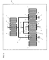
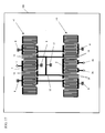
- Fig. 7 is a plan view showing a SAW filter in accordance with a second embodiment of the present invention.
- the shield electrode 12 includes two comb-like shield electrodes 14 that are connected to the earth potential 13.
- One of the two comb-like shield electrodes 14 is arranged between IDTs 4 and 5, and the other is arranged between IDTs 4 and 6.
- the lengths of electrode fingers of the comb-like electrodes 14 are substantially equal to those of the IDTs 4 though 6, which are vertical to the propagation direction of the SAW.
- the IDT 4 and the IDT 5 do not face each other.
- the IDT 4 and the IDT 6 do not face each other, either.
- the comb-like shield electrode 14 includes two electrode fingers. However, the number of electrode fingers may be one, or may be equal to or greater than three.
- the comb-like shield electrode 14 may be longer than that shown in Fig. 7.
- Fig. 8 is a graph showing the amplitude symmetry of the second embodiment of the present invention and the comparative example in Fig. 2.
- Fig. 9 is a graph showing the phase symmetry of the second embodiment of the present invention and the comparative example.
- the horizontal axes in Figs. 8 and 9 denote frequency (MHz).
- the vertical axis in Fig. 8 denotes frequency symmetry (dB) and the vertical axis in Fig. 9 denotes phase symmetry (degree).
- 0.0 defines the perfect symmetry. As shown in Figs. 8 and 9, it has been found that both the frequency symmetry and phase symmetry are considerably improved.
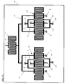
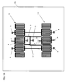
- Fig. 12 is a plan view of a SAW filter in accordance with a third embodiment of the present invention.
- Two filters 30 and 130 are connected in parallel.
- the balanced operation is performed between the terminal 2a of the filter 30 and the terminal 2b of the filter 130.
- the filter 30 has the same components and configuration as those of the SAW filter shown in Fig. 1, and includes the shield electrode 12.
- the filters 30 and 130 have mutually different electrode finger patterns so as to operate in opposite phases. Specifically, the IDT 4 of the filter 30 has a different electrode finger pattern from that of the filter 130.
- the filter 130 also includes the shield electrode 12 as shown.
- the distance between bus bars 4a and 5a of the filter 130 is longer than its corresponding distance of the filter 30. This results from the electrode finger pattern of the filter 130.
- An edge 12e of the shield electrode 12 of the filter 130 is widely arranged. Thus, an excellent symmetry of the balanced operation is obtainable by the function of the shield electrode 12.
- Two earth potentials 13 in Fig. 12 are in circuitries different from those of ground potentials 8.
- the two earth potentials 13 are connected together on a package on which the piezoelectric substrate 100 is mounted, and are connected to one external connection terminal for the earth potential.
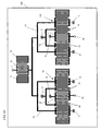
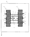
- Fig. 13 is a plan view of a SAW filter in accordance with a fourth embodiment of the present invention.
- a shield electrode 12A is added to the third embodiment of the present invention.
- Each of filters 30 and 130 includes the shield electrode 12A on the opposite side of shield electrodes 12 in order to establish shielding between IDTs 4 and 5 and between IDTs 4 and 6.
- the shield electrode 12A is connected to the earth potential 13A. It is thus possible to further improve the symmetry of the balanced operation, by providing the shield electrodes 12 and 12A on both sides of the IDTs 4 through 6 that are arranged in line.
- the earth potentials 13A are separately arranged and are respectively connected to the two shield electrodes 12A. However, the earth potentials 13A may be connected together on the piezoelectric substrate 100 and then may be connected to the earth potential.
- the shield electrodes 12 and 12A may be provided on both sides of the IDTs 4 through 6, which are arranged in line.
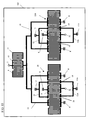
- Fig. 14 is a plan view of a SAW filter in accordance with a fifth embodiment of the present invention.
- the fifth embodiment of the present invention includes the two shield electrodes 12 in Fig. 12, and also includes the same type of comb-like electrodes as those in Fig. 7.
- Fig. 15 is a plan view of a SAW filter in accordance with a sixth embodiment of the present invention.
- the sixth embodiment of the present invention includes the four shield electrodes 12 in Fig. 13, and also includes the same type of comb-like electrodes as those in Fig. 7. Adjacent electrode fingers of the shield electrode 12 are all connected together.
- the shield electrodes 12 and 12A of the filter 30 are formed in a loop so as to surround the IDT 4.
- the shield electrodes 12 and 12A of the filter 130 are arranged in a loop so as to surround another IDT 4.
- Earth potentials 13A are respectively connected to the shield electrode 12A as shown in Fig. 15, but may be connected together on the piezoelectric substrate 100, and then may be connected to the earth potential.
- Fig. 16 is a plan view of a SAW filter in accordance with a seventh embodiment of the present invention.
- This filter includes two filters 40 and 140.
- the filter 40 outputs balanced signals to the filter 140, which outputs the balanced signals through balanced signal terminals 2a and 2b.
- the IDT 4 of the filter 140 includes two IDTs, which are connected together to one of bus bars and are adjacently arranged in a propagation direction.
- the shield electrode 12 is provided to be connected by the filters 40 and 140. Edges of the shield electrode 12 are arranged between adjacent bus bars.
- the shield electrode 12 is connected to the earth potential in a circuitry, which is different from that of the ground potential 8.
- Fig. 17 is a plan view of a SAW filter in accordance with an eighth embodiment of the present invention.
- the eighth embodiment of the present invention includes the shield electrodes 12 in accordance with the seventh embodiment of the present invention as shown in Fig. 16, and also includes the same type of comb-like electrodes as those in Fig. 7.
- Fig. 18 is a plan view of a SAW filter in accordance with a ninth embodiment of the present invention.
- the ninth embodiment of the present invention is a modified example of the seventh embodiment of the present invention as shown in Fig. 16.
- the ninth embodiment of the present invention includes an IDT 4, which has an electrode pattern different from that of the IDT 4 employed in the seventh embodiment of the present invention.
- the IDT 4 used in the ninth embodiment includes a pair of comb-like electrodes to which balanced signal terminals 2a and 2b are respectively connected.
- the shield electrode 12 has the same configuration as that in Fig. 7.
- Fig. 19 is a plan view of a SAW filter in accordance with a tenth embodiment of the present invention.
- This embodiment includes the shield electrodes 12 employed in the seventh embodiment of as shown in Fig. 18, and also includes the same type of comb-like electrodes as those in Fig. 7.
- the shield electrode 12 may be made of the same material as those of the IDTs 4 through 6, for example, aluminum or aluminum-copper alloy, and may be made at the same time.
- the above-mentioned embodiments are employed together as necessary.
- the pads, which are provided on the piezoelectric substrate 100 as shown in Figs. 5 and 6, may be applied to the fifth through tenth embodiments.
- the shield electrode may be arranged between the input IDT and the output IDT, or between the interconnection lines that connect the input and output IDTs.
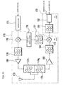
- Fig. 20 is a block diagram illustrating a wireless device in accordance with an eleventh embodiment. This wireless device is equipped with some SAW filters of the present invention. Fig. 20 shows transmission and reception systems of the wireless device. In the case where the wireless device is a mobile telephone or the like, the transmission and reception systems in Fig. 20 are connected to a speech processing system or the like.
- the wireless device includes an RF (Radio Frequency) unit 170, a modulator 171, and an IF (Intermediate Frequency) unit 172.
- the RF unit 170 includes an antenna 173, a separator 174, a low noise amplifier 183, an interstage filter 184, a mixer (multiplier) 175, a local oscillator 176, an interstage filter 177, a mixer (multiplier) 178, an interstage filter 179, and a power amplifier 180.
- An audio signal applied from the speech processing system is modulated on the modulator 171, and the frequency of the audio signal is converted or mixed on the mixer 178 of the RF unit 170 with the use of an oscillation signal generated by the local oscillator 176.
- the separator 174 includes a transmission filter 174 1 , a reception filter 174 2 , and a matching circuit (not shown).
- the separator 174 utilizes the SAW filter(s) of the present invention.
- a signal transmitted from the power amplifier 180 is fed to the antenna 173 through the separator 174.
- the signal received from the antenna 173 passes through the reception filter 174 2 of the separator 174, and is applied to the mixer 175 through the low noise amplifier 183 and the interstage filter 184.
- the mixer 175 receives an oscillating frequency generated by the local oscillator 176 by way of the interstage filter 177, converts the frequency of the received signal, and applies the signal to the IF unit 172.
- the IF unit 172 receives the signal by way of the IF filter 181, demodulates with a demodulator 182, and outputs the demodulated audio signal to the speech processing system that is not shown.
- the SAW filter of the present invention includes the above-mentioned separator 174 and the interstage filters 177, 179, and 184.
- the above-mentioned separator 174 includes the transmission filter 174 1 and the reception filter 174 2 .
- the SAW filter of the present invention is capable of decreasing malfunctions caused by noises in a high-frequency circuit of the wireless device on which an integrated circuit (IC) having an input and output of the balanced operation.
- IC integrated circuit
Landscapes
- Physics & Mathematics (AREA)
- Acoustics & Sound (AREA)
- Electromagnetism (AREA)
- Surface Acoustic Wave Elements And Circuit Networks Thereof (AREA)
Applications Claiming Priority (2)
| Application Number | Priority Date | Filing Date | Title |
|---|---|---|---|
| JP2003392832 | 2003-11-21 | ||
| JP2003392832A JP4291115B2 (ja) | 2003-11-21 | 2003-11-21 | 弾性表面波フィルタ及びそれを用いた無線装置 |
Publications (2)
| Publication Number | Publication Date |
|---|---|
| EP1533895A2 true EP1533895A2 (de) | 2005-05-25 |
| EP1533895A3 EP1533895A3 (de) | 2010-01-06 |
Family
ID=34431641
Family Applications (1)
| Application Number | Title | Priority Date | Filing Date |
|---|---|---|---|
| EP04257181A Withdrawn EP1533895A3 (de) | 2003-11-21 | 2004-11-19 | Oberflächenwellenfilter und Funkgerät mit einem derartigen Filter |
Country Status (5)
| Country | Link |
|---|---|
| US (1) | US7292122B2 (de) |
| EP (1) | EP1533895A3 (de) |
| JP (1) | JP4291115B2 (de) |
| KR (1) | KR100667126B1 (de) |
| CN (1) | CN1619957B (de) |
Cited By (1)
| Publication number | Priority date | Publication date | Assignee | Title |
|---|---|---|---|---|
| EP1783901A3 (de) * | 2005-10-26 | 2008-01-23 | Fujitsu Media Devices Limited | Akustisches Oberflächenwellenbauelement |
Families Citing this family (9)
| Publication number | Priority date | Publication date | Assignee | Title |
|---|---|---|---|---|
| US7287431B2 (en) * | 2005-04-14 | 2007-10-30 | Honeywell International Inc. | Wireless oil filter sensor |
| JP2006311041A (ja) * | 2005-04-27 | 2006-11-09 | Matsushita Electric Ind Co Ltd | アンテナ共用器 |
| WO2008038498A1 (fr) * | 2006-09-28 | 2008-04-03 | Murata Manufacturing Co., Ltd. | Dispositif de filtre d'onde acoustique équilibré |
| DE102010008774B4 (de) * | 2010-02-22 | 2015-07-23 | Epcos Ag | Mikroakustisches Filter mit kompensiertem Übersprechen und Verfahren zur Kompensation |
| JP2012065272A (ja) * | 2010-09-17 | 2012-03-29 | Nippon Dempa Kogyo Co Ltd | 弾性波デバイス |
| JP6558445B2 (ja) * | 2015-11-18 | 2019-08-14 | 株式会社村田製作所 | 弾性波フィルタ、デュプレクサ及び弾性波フィルタモジュール |
| JP7341641B2 (ja) * | 2018-08-24 | 2023-09-11 | 太陽誘電株式会社 | マルチプレクサ |
| US20230027129A1 (en) * | 2021-07-20 | 2023-01-26 | Skyworks Solutions, Inc. | Acoustic wave devices with thermal bypass |
| CN120294637B (zh) * | 2025-04-08 | 2025-11-07 | 北京深谋科技有限公司 | 一种基于声表面波模态局域化的磁敏传感器 |
Citations (2)
| Publication number | Priority date | Publication date | Assignee | Title |
|---|---|---|---|---|
| EP0605884A1 (de) * | 1993-01-05 | 1994-07-13 | Murata Manufacturing Co., Ltd. | Akustische Oberflächenwellenanordnung von IIDT-Typ |
| JPH1197966A (ja) * | 1997-09-22 | 1999-04-09 | Tdk Corp | 弾性表面波フィルタ |
Family Cites Families (11)
| Publication number | Priority date | Publication date | Assignee | Title |
|---|---|---|---|---|
| JPS6055715A (ja) * | 1983-09-07 | 1985-04-01 | Toshiba Corp | 弾性表面波装置 |
| JPH02104013A (ja) * | 1988-10-13 | 1990-04-17 | Toshiba Corp | 弾性表面波装置 |
| US5710529A (en) * | 1993-10-15 | 1998-01-20 | Ngk Insulators, Ltd. | Surface acoustic wave filer device having a cascade filter structure and a piezoelectric substrate having mirror-polished surfaces |
| DE69938989D1 (de) * | 1998-05-29 | 2008-08-14 | Fujitsu Ltd | Akustisches Oberflächenwellenfilter mit verbesserter Unterdrückung ausserhalb eines Durchlassbereichs |
| JP2000031777A (ja) | 1998-07-14 | 2000-01-28 | Toyo Commun Equip Co Ltd | トランスバーサル型弾性表面波フィルタ |
| TW483238B (en) * | 2000-06-30 | 2002-04-11 | Fujitsu Media Devices Ltd | Surface acoustic wave device |
| JP3454239B2 (ja) * | 2000-08-31 | 2003-10-06 | 株式会社村田製作所 | 弾性表面波フィルタ |
| JP3384403B2 (ja) * | 2001-03-01 | 2003-03-10 | 株式会社村田製作所 | 弾性表面波装置、通信装置 |
| JP3864850B2 (ja) * | 2001-08-09 | 2007-01-10 | 株式会社村田製作所 | 弾性表面波フィルタ、通信装置 |
| JP2003209456A (ja) * | 2002-01-16 | 2003-07-25 | Toyo Commun Equip Co Ltd | Sawフィルタ |
| JP3757893B2 (ja) * | 2002-04-10 | 2006-03-22 | 株式会社村田製作所 | 弾性表面波装置、および、これを搭載した通信装置 |
-
2003
- 2003-11-21 JP JP2003392832A patent/JP4291115B2/ja not_active Expired - Lifetime
-
2004
- 2004-11-19 KR KR1020040095121A patent/KR100667126B1/ko not_active Expired - Fee Related
- 2004-11-19 US US10/992,116 patent/US7292122B2/en not_active Expired - Lifetime
- 2004-11-19 EP EP04257181A patent/EP1533895A3/de not_active Withdrawn
- 2004-11-19 CN CN2004100913196A patent/CN1619957B/zh not_active Expired - Fee Related
Patent Citations (2)
| Publication number | Priority date | Publication date | Assignee | Title |
|---|---|---|---|---|
| EP0605884A1 (de) * | 1993-01-05 | 1994-07-13 | Murata Manufacturing Co., Ltd. | Akustische Oberflächenwellenanordnung von IIDT-Typ |
| JPH1197966A (ja) * | 1997-09-22 | 1999-04-09 | Tdk Corp | 弾性表面波フィルタ |
Cited By (2)
| Publication number | Priority date | Publication date | Assignee | Title |
|---|---|---|---|---|
| EP1783901A3 (de) * | 2005-10-26 | 2008-01-23 | Fujitsu Media Devices Limited | Akustisches Oberflächenwellenbauelement |
| US7515017B2 (en) | 2005-10-26 | 2009-04-07 | Fujitsu Media Devices Limited | Surface acoustic wave device utilizing a terminal routing pattern |
Also Published As
| Publication number | Publication date |
|---|---|
| US7292122B2 (en) | 2007-11-06 |
| EP1533895A3 (de) | 2010-01-06 |
| KR100667126B1 (ko) | 2007-01-12 |
| JP4291115B2 (ja) | 2009-07-08 |
| JP2005159563A (ja) | 2005-06-16 |
| CN1619957A (zh) | 2005-05-25 |
| CN1619957B (zh) | 2011-06-15 |
| US20050110599A1 (en) | 2005-05-26 |
| KR20050049399A (ko) | 2005-05-25 |
Similar Documents
| Publication | Publication Date | Title |
|---|---|---|
| US6483402B2 (en) | Surface acoustic wave device | |
| US7283016B2 (en) | Balanced acoustic wave filter and acoustic wave filter | |
| US7659796B2 (en) | Surface acoustic wave device and duplexer and communication device using the same | |
| US7902940B2 (en) | Duplexer | |
| EP1670138B1 (de) | Akustischer wellenfilter und kommunikationseinheit | |
| US7915972B2 (en) | Balance filter and duplexer | |
| KR100494049B1 (ko) | 탄성표면파 필터 및 통신 장치 | |
| JP2001326557A (ja) | 弾性表面波装置 | |
| KR20020003077A (ko) | 탄성표면파 장치 | |
| US20020167378A1 (en) | Surface acoustic wave filter apparatus and communication apparatus | |
| CN101971496A (zh) | 弹性波滤波器、使用其的双工器以及电子设备 | |
| JP4541853B2 (ja) | アンテナ分波器およびアンテナ分波器用表面弾性波フィルタ | |
| US7292122B2 (en) | Surface acoustic wave filter and wireless device that employs the same | |
| CN111162756A (zh) | 多工器 | |
| US6597262B2 (en) | Surface acoustic wave filter and communication apparatus incorporating the same | |
| JP2003124777A (ja) | 弾性表面波装置 | |
| US7800460B2 (en) | Elastic wave filter device and duplexer | |
| US6963156B2 (en) | Surface acoustic wave device and communication device incorporating same | |
| CN112448693B (zh) | 滤波器模块 | |
| WO2018206264A1 (en) | Saw device with suppressed parasitic signal |
Legal Events
| Date | Code | Title | Description |
|---|---|---|---|
| PUAI | Public reference made under article 153(3) epc to a published international application that has entered the european phase |
Free format text: ORIGINAL CODE: 0009012 |
|
| AK | Designated contracting states |
Kind code of ref document: A2 Designated state(s): AT BE BG CH CY CZ DE DK EE ES FI FR GB GR HU IE IS IT LI LU MC NL PL PT RO SE SI SK TR |
|
| AX | Request for extension of the european patent |
Extension state: AL HR LT LV MK YU |
|
| PUAL | Search report despatched |
Free format text: ORIGINAL CODE: 0009013 |
|
| AK | Designated contracting states |
Kind code of ref document: A3 Designated state(s): AT BE BG CH CY CZ DE DK EE ES FI FR GB GR HU IE IS IT LI LU MC NL PL PT RO SE SI SK TR |
|
| AX | Request for extension of the european patent |
Extension state: AL HR LT LV MK YU |
|
| RIC1 | Information provided on ipc code assigned before grant |
Ipc: H03H 9/02 20060101ALI20091127BHEP Ipc: H03H 9/00 20060101AFI20050221BHEP |
|
| 17P | Request for examination filed |
Effective date: 20100630 |
|
| AKX | Designation fees paid |
Designated state(s): DE FR |
|
| 17Q | First examination report despatched |
Effective date: 20100830 |
|
| RAP1 | Party data changed (applicant data changed or rights of an application transferred) |
Owner name: TAIYO YUDEN CO., LTD. |
|
| STAA | Information on the status of an ep patent application or granted ep patent |
Free format text: STATUS: THE APPLICATION IS DEEMED TO BE WITHDRAWN |
|
| 18D | Application deemed to be withdrawn |
Effective date: 20140409 |