EP1529642B1 - Ink jet apparatus - Google Patents
Ink jet apparatus Download PDFInfo
- Publication number
- EP1529642B1 EP1529642B1 EP04026226A EP04026226A EP1529642B1 EP 1529642 B1 EP1529642 B1 EP 1529642B1 EP 04026226 A EP04026226 A EP 04026226A EP 04026226 A EP04026226 A EP 04026226A EP 1529642 B1 EP1529642 B1 EP 1529642B1
- Authority
- EP
- European Patent Office
- Prior art keywords
- layer
- conformal
- raised contact
- microinches
- emitting apparatus
- Prior art date
- Legal status (The legal status is an assumption and is not a legal conclusion. Google has not performed a legal analysis and makes no representation as to the accuracy of the status listed.)
- Expired - Fee Related
Links
Images

Classifications
-
- B—PERFORMING OPERATIONS; TRANSPORTING
- B41—PRINTING; LINING MACHINES; TYPEWRITERS; STAMPS
- B41J—TYPEWRITERS; SELECTIVE PRINTING MECHANISMS, i.e. MECHANISMS PRINTING OTHERWISE THAN FROM A FORME; CORRECTION OF TYPOGRAPHICAL ERRORS
- B41J2/00—Typewriters or selective printing mechanisms characterised by the printing or marking process for which they are designed
- B41J2/005—Typewriters or selective printing mechanisms characterised by the printing or marking process for which they are designed characterised by bringing liquid or particles selectively into contact with a printing material
- B41J2/01—Ink jet
- B41J2/135—Nozzles
- B41J2/14—Structure thereof only for on-demand ink jet heads
- B41J2/14201—Structure of print heads with piezoelectric elements
- B41J2/14233—Structure of print heads with piezoelectric elements of film type, deformed by bending and disposed on a diaphragm
-
- Y—GENERAL TAGGING OF NEW TECHNOLOGICAL DEVELOPMENTS; GENERAL TAGGING OF CROSS-SECTIONAL TECHNOLOGIES SPANNING OVER SEVERAL SECTIONS OF THE IPC; TECHNICAL SUBJECTS COVERED BY FORMER USPC CROSS-REFERENCE ART COLLECTIONS [XRACs] AND DIGESTS
- Y10—TECHNICAL SUBJECTS COVERED BY FORMER USPC
- Y10T—TECHNICAL SUBJECTS COVERED BY FORMER US CLASSIFICATION
- Y10T29/00—Metal working
- Y10T29/49—Method of mechanical manufacture
- Y10T29/49401—Fluid pattern dispersing device making, e.g., ink jet
Definitions
- the subject disclosure is generally directed to drop emitting apparatus, and more particularly to ink jet apparatus.
- Drop on demand ink jet technology for producing printed media has been employed in commercial products such as printers, plotters, and facsimile machines.
- an ink jet image is formed by selective placement on a receiver surface of ink drops emitted by a plurality of drop generators implemented in a printhead or a printhead assembly.
- the printhead assembly and the receiver surface are caused to move relative to each other, and drop generators are controlled to emit drops at appropriate times, for example by an appropriate controller.
- the receiver surface can be a transfer surface or a print medium such as paper. In the case of a transfer surface, the image printed thereon is subsequently transferred to an output print medium such as paper.
- a known ink jet printhead structure employs electromechanical transducers that are attached to a metal diaphragm plate, and it can be difficult to make electrical connections to the electromechanical transducers.
- US4516140 discloses an inkjet printer having a fluid channel layer and a diaphragm disposed on this channel layer. Piezoelectric actuators are adhesively attached to a thin film circuit having raised contact regions.
- the present invention provides a drop emitting apparatus as defined in claim 1 and a drop generator as defined in claim 10. Embodiments are set forth in the dependent claims.
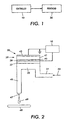
- FIG. 1 is a schematic block diagram of an embodiment of a drop-on-demand drop emitting apparatus.
- FIG. 2 is a schematic block diagram of an embodiment of a drop generator that can be employed in the drop emitting apparatus of FIG. 1.
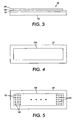
- FIG. 3 is a schematic elevational view of an embodiment of an ink jet printhead assembly.
- FIG. 4 is a schematic plan view of an embodiment of a diaphragm layer of the ink jet printhead assembly of FIG. 3.
- FIG. 5 is a schematic plan view of an embodiment of a thin film interconnect circuit of the ink jet printhead assembly of FIG. 3.
- FIG. 6 is a schematic elevational sectional view of a portion of an embodiment of a thin film interconnect circuit of the ink jet printhead assembly.
- FIG. 7 is a schematic elevational sectional view of a portion of another embodiment of a thin film interconnect circuit of the ink jet printhead assembly.
- FIG. 8 is a schematic elevational sectional view of a portion of a further embodiment of a thin film interconnect circuit of the ink jet printhead assembly.
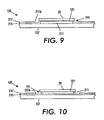
- FIG. 9 is a schematic elevational sectional view of a portion of an embodiment of a thin film interconnect circuit of the ink jet printhead assembly.
- FIG. 10 is a schematic elevational sectional view of a portion of another embodiment of a thin film interconnect circuit of the ink jet printhead assembly.
- FIG. 1 is a schematic block diagram of an embodiment of a drop-on-demand printing apparatus that includes a controller 10 and a printhead assembly 20 that can include a plurality of drop emitting drop generators.
- the controller 10 selectively energizes the drop generators by providing a respective drive signal to each drop generator.
- Each of the drop generators can employ a piezoelectric transducer such as a ceramic piezoelectric transducer.
- each of the drop generators can employ a shear-mode transducer, an annular constrictive transducer, an electrostrictive transducer, an electromagnetic transducer, or a magnetorestrictive transducer.
- the printhead assembly 20 can be formed of a stack of laminated sheets or plates, such as of stainless steel.
- FIG. 2 is a schematic block diagram of an embodiment of a drop generator 30 that can be employed in the printhead assembly 20 of the printing apparatus shown in FIG. 1.
- the drop generator 30 includes an inlet channel 31 that receives ink 33 from a manifold, reservoir or other ink containing structure.
- the ink 33 flows into a pressure or pump chamber 35 that is bounded on one side, for example, by a flexible diaphragm 37.
- a thin-film interconnect structure 38 is attached to the flexible diaphragm, for example so as to overlie the pressure chamber 35.
- An electromechanical transducer 39 is attached to the thin film interconnect structure 38.
- the electromechanical transducer 39 can be a piezoelectric transducer that includes a piezo element 41 disposed for example between electrodes 42 and 43 that receive drop firing and non-firing signals from the controller 10 via the thin-film interconnect structure 38, for example.
- the electrode 43 is connected to ground in common with the controller 10, while the electrode 42 is actively driven to actuate the electromechanical transducer 41 through the interconnect structure 38.
- Actuation of the electromechanical transducer 39 causes ink to flow from the pressure chamber 35 to a drop forming outlet channel 45, from which an ink drop 49 is emitted toward a receiver medium 48 that can be a transfer surface, for example.
- the outlet channel 45 can include a nozzle or orifice 47.
- the ink 33 can be melted or phase changed solid ink, and the electromechanical transducer 39 can be a piezoelectric transducer that is operated in a bending mode, for example.
- FIG. 3 is a schematic elevational view of an embodiment of an ink jet printhead assembly 20 that can implement a plurality of drop generators 30 (FIG. 2), for example as an array of drop generators.
- the ink jet printhead assembly includes a fluid channel layer or substructure 131, a diaphragm layer 137 attached to the fluid channel layer 131, a thin-film interconnect circuit layer 138 disposed on the diaphragm layer 137 and a transducer layer 139 attached to the thin-film interconnect circuit layer 138.
- the fluid channel layer 131 implements the fluid channels and chambers of the drop generators 30, while the diaphragm layer 137 implements the diaphragms 37 of the drop generators.
- the thin-film interconnect circuit layer 138 implements the interconnect circuits 38, while the transducer layer 139 implements the electromechanical transducers 39 of the drop generators 30.
- the diaphragm layer 137 comprises a metal plate or sheet such as stainless steel that is attached or bonded to the fluid channel layer 131.
- the diaphragm layer 137 can also comprise an electrically non-conductive material such as a ceramic.
- the fluid channel layer 131 can comprise multiple laminated plates or sheets.
- the transducer layer 139 can comprise an array of kerfed ceramic transducers that are attached or bonded to the thin film interconnect circuit layer 138 by a suitable adhesive.
- asperity contacts are more particularly formed between the transducer layer 139 and the thin film interconnect layer 138, and the adhesive can comprise a low conductivity adhesive.
- an epoxy, acrylic, or phenolic adhesive can be used..
- FIG. 4 is a schematic plan view of an embodiment of a diaphragm layer 137 that includes a roughened, non-smooth bonding region 137A formed by particle blasting such as sand blasting, or by laser roughening, for example.
- the bonding region 137A can have a roughness average (Ra) in the range of about 1 microinch to about 100 microinches, for example.
- the bonding region 137A can have a roughness average in the range of about 5 microinches to about 20 microinches.
- the bonding region 137A can have a roughness average in the range of about 50 microinches to about 100 microinches.
- FIG. 5 is a schematic plan view of an embodiment of a thin film interconnect circuit layer 138 that includes conformal raised contact pads or regions 191 disposed over the roughened bonding region 137A (FIG. 4) of the diaphragm layer 137, wherein top surfaces of the raised contact regions 191 have a roughness that generally conforms to the roughness of the underlying roughened bonding region 137A of the diaphragm layer 137.
- the electromechanical transducers 39 (FIGS. 6-10) are attached to respective conformal raised contact pads 191 by a thin layer of adhesive, and asperity contacts are formed between the top surfaces of the raised contact portions 191 and the electromechanical transducers 39. As disclosed in various embodiments illustrated in FIGS.
- the conformal raised contact regions 191 can be formed by a thin film structure that can include for example a mesa layer and a patterned conductive layer.
- the layers of the thin film stack that form the conformal raised contact regions 191 are preferably conformal such that the top surfaces of the raised contact regions 191 have a roughness that generally conforms to the roughness of the underlying roughened bonding region 137A of the diaphragm layer 137.
- the top surfaces of the conformal raised contact regions 191 have a roughness average (Ra) in the range of about 1 microinch to about 100 microinches, which can be achieved for example by configuring the roughened bonding region 137A to have a suitable roughness.
- the top surfaces of the conformal raised contact regions 191 can have a roughness average in the range of about 5 microinches to about 20 microinches. Still further, the top surfaces of the raised conformal contact regions 191 can have a roughness average in the range of about 30 microinches to about 80 microinches.
- the thin film interconnect circuit 138 can provide for electrical interconnection to the individual electromechanical transducers 39.
- FIG. 6 is a schematic elevational sectional view of a portion of an embodiment of a thin film interconnect circuit layer 138 that can be used with an electrically conductive or non-conductive diaphragm layer 137.
- the thin film interconnect circuit layer 138 includes a conformal mesa layer 211 comprising a plurality of mesas, a conformal blanket dielectric layer 213 overlying the mesa layer 211 and the diaphragm layer 137, and a patterned conformal conductive layer 215 disposed on the blanket dielectric layer 213.
- the blanket dielectric layer serves to electrically isolate the diaphragm layer 137 from the patterned conformal conductive layer 215.
- the mesa layer 211 can be electrically non-conductive (e.g., dielectric) or conductive (e.g., metal).
- the mesas and the overlying portions of the conformal blanket dielectric layer 213 and the patterned conformal conductive layer 215 form raised contact regions or pads 191.
- the thin film interconnect circuit layer 138 can further include a patterned dielectric layer 217 having openings 217A through which the raised contact pads 191 extend.
- the raised contact pads 191 are higher than the other layers of the thin film interconnect circuit layer 138, and comprise the highest portions of the interconnect layer 138. This facilitates the attachment of an electromechanical transducer 39 to each of the raised contact pads 191.
- the conformal mesa layer 211 can comprise a suitably patterned conformal dielectric layer or conformal metal layer, for example.
- the patterned conformal conductive layer 215 can comprise a patterned conformal metal layer.
- the top surfaces of the raised contact pads 191 have a roughness that generally conforms to the roughened surface of the bonding region 137A of the metal diaphragm 137.
- the top surfaces of the raised contact pads 191 comprise roughened surfaces.
- the electromechanical transducers 39 are attached to respective contact pads 191 by a thin adhesive layer 221 that is sufficiently thin such that asperity contacts are formed between the top surface of the contact pads and the electromechanical transducers 39. Asperity contacts are more particularly formed by high points of the contact pads 191 that pass through the thin adhesive layer and contact the electromechanical transducers 39.
- FIG. 7 is a schematic elevational sectional view of a portion of a further embodiment of a thin film interconnect circuit layer 138 that can be used with an electrically conductive or non-conductive diaphragm layer 137.
- the thin film interconnect circuit layer 138 includes a conformal blanket dielectric layer 213, a conformal patterned conductive layer 215 disposed on the conformal blanket dielectric layer 213, and a conformal conductive mesa layer 211 comprising a plurality of conductive mesas overlying the patterned conformal conductive layer 215.
- the conductive mesas and the underlying portions of the conformal conductive layer 215 form raised contact regions or pads 191.
- the interconnect circuit layer 138 can further include a patterned dielectric layer 217 having openings 217A through which the raised contact pads 191 extend.
- the raised contact pads 191 are higher than the other layers of the interconnect circuit layer 138, and comprise the highest portions of the interconnect circuit layer 138. This facilitates the attachment of an electromechanical transducer 39 to each of the raised contact pads 191.
- the patterned conformal mesa layer 211 can comprise a suitably patterned conformal metal layer
- the patterned conformal conductive layer 215 can also comprise a suitably patterned conformal metal layer, for example.
- the top surfaces of the raised contact pads 191 have a roughness that generally conforms to the roughened surface of the bonding region 137A of the metal diaphragm 137.
- the electromechanical transducers 39 are attached to respective contact pads 191 by a thin adhesive layer 221 that is sufficiently thin such that asperity contacts are formed between the top surfaces of the raised contact pads 191 and the electromechanical transducers 39.
- FIG. 8 is a schematic elevational sectional view of a portion of a further embodiment of a thin film interconnect circuit layer 138 that can be used with an electrically conductive or non-conductive diaphragm 137.
- the interconnect circuit layer 138 includes a conformal blanket dielectric layer 213, a mesa layer 211 comprising a plurality of mesas overlying the conformal blanket dielectric layer 213, and a conformal patterned conductive layer 215 overlying the mesa layer 211.
- the mesa layer 211 can be electrically non-conductive (e.g., dielectric) or conductive (e.g., metal).
- the mesas and the overlying portions of the patterned conformal conductive layer 215 form raised contact regions or pads 191.
- the thin film interconnect circuit layer 138 can further include a patterned dielectric layer 217 having openings 217A through which the raised contact pads 191 extend.
- the raised contact pads 191 are higher than the other layers of the interconnect circuit layer 138, and comprise the highest portions of the interconnect layer 138. This facilitates the attachment of an electromechanical transducer 39 to each of the raised contact pads 191.
- the conformal mesa layer 211 can comprise a suitably patterned conformal dielectric layer or conformal metal layer, for example.
- the patterned conformal conductive layer 215 can comprise a patterned conformal metal layer.
- the top surfaces of the raised contact pads 191 have a roughness that generally conforms to the roughened surface of the bonding region 137A of the metal diaphragm 137.
- the electromechanical transducers 39 are attached to respective contact pads 191 by a thin adhesive layer 221 that is sufficiently thin such that asperity contacts are formed between the top surfaces of the raised contact pads 191 and the electromechanical transducers 39.
- FIG. 9 is a schematic elevational sectional view of a portion of an embodiment of a thin film interconnect circuit layer 138 that can be used with an electrically non-conductive diaphragm 137.
- the thin film interconnect circuit layer 138 includes a conformal mesa layer 211 comprising a plurality of mesas disposed on the bonding region 137A of the electrically non-conductive diaphragm 137, and a patterned conformal conductive layer 215 overlying the mesa layer 211.
- the mesa layer 211 can be electrically non-conductive (e.g., dielectric) or conductive (e.g., metal).
- the mesas and the overlying portions of the patterned conformal conductive layer 215 form raised contact regions or pads 191.
- the thin film interconnect circuit layer 138 can further include a patterned dielectric layer 217 having openings 217A through which the raised contact pads 191 extend.
- the raised contact pads 191 are higher than the other layers of the interconnect layer 138, and comprise the highest portions of the interconnect layer 138. This facilitates the attachment of an electromechanical transducer 39 to each of the raised contact pads 191.
- the conformal mesa layer 211 can comprise a suitably patterned conformal dielectric layer or patterned conformal metal layer, for example.
- the patterned conformal conductive layer 215 can comprise a patterned conformal metal layer, for example.
- the top surfaces of the raised contact pads 191 have a roughness that generally conforms to the roughened surface of the bonding region 137A of the metal diaphragm 137.
- the electromechanical transducers 39 are attached to respective contact pads 191 by a thin adhesive layer 221 that is sufficiently thin such that asperity contacts are formed between the top surfaces of the raised contact pads 191 and the electromechanical transducers 39.
- FIG. 10 is a schematic elevational sectional view of a portion of a further embodiment of a thin film interconnect circuit layer 138 that can be used with an electrically non-conductive diaphragm layer 137.
- the thin film interconnect circuit layer 138 includes a patterned conformal conductive layer 215 and a conductive mesa layer 211 comprising a plurality of mesas overlying the patterned conformal conductive layer 215.
- the conductive mesas and the underlying portions of the patterned conformal conductive layer 215 form raised contact regions or pads 191.
- the thin film interconnect circuit layer 138 can further include a patterned dielectric layer 217 having openings 217A through which the raised contact pads 191 extend.
- the raised contact pads 191 are higher than the other layers of the thin film interconnect circuit layer 138, and comprise the highest portions of the interconnect layer 138. This facilitates the attachment of an electromechanical transducer 39 to each of the raised contact pads 191.
- the patterned conformal conductive mesa layer 211 can comprise a suitably patterned conformal metal layer, and the patterned conformal conductive layer 215 can also comprise a suitably patterned conformal metal layer, for example.
- the top surfaces of the raised contact pads 191 have a roughness that generally conforms to the roughened surface of the bonding region 137A of the metal diaphragm 137.
- the electromechanical transducers 39 are attached to respective contact pads 191 by a thin adhesive layer 221 that is sufficiently thin such that asperity contacts are formed between the top surfaces of the raised contact pads 191 and the electromechanical transducers 39.
- Each dielectric layer of the thin film interconnect circuit layer 138 can comprise silicon oxide, silicon nitride, or silicon oxynitride, for example, and can have a thickness in the range of about 0.1 micrometers of about 5 micrometers. More specifically, each dielectric layer can have a thickness in the range of about 1 micrometers to about 2 micrometers.
- Each conductive layer of the thin film interconnect circuit layer 138 can comprise aluminum, chromium, nickel, tantalum or copper, for example, and can have a thickness in the range of about 0.1 micrometers of about 5 micrometers. More specifically, each conductive layer can have a thickness in the range of about 1 micrometers to about 2 micrometers.
Landscapes
- Particle Formation And Scattering Control In Inkjet Printers (AREA)
- Micromachines (AREA)
Applications Claiming Priority (2)
| Application Number | Priority Date | Filing Date | Title |
|---|---|---|---|
| US702247 | 2003-11-05 | ||
| US10/702,247 US7048361B2 (en) | 2003-11-05 | 2003-11-05 | Ink jet apparatus |
Publications (2)
| Publication Number | Publication Date |
|---|---|
| EP1529642A1 EP1529642A1 (en) | 2005-05-11 |
| EP1529642B1 true EP1529642B1 (en) | 2006-10-18 |
Family
ID=34435546
Family Applications (1)
| Application Number | Title | Priority Date | Filing Date |
|---|---|---|---|
| EP04026226A Expired - Fee Related EP1529642B1 (en) | 2003-11-05 | 2004-11-04 | Ink jet apparatus |
Country Status (7)
| Country | Link |
|---|---|
| US (1) | US7048361B2 (ja) |
| EP (1) | EP1529642B1 (ja) |
| JP (1) | JP4597633B2 (ja) |
| CN (1) | CN100415515C (ja) |
| BR (1) | BRPI0404831A (ja) |
| CA (1) | CA2486454C (ja) |
| DE (1) | DE602004002827T2 (ja) |
Families Citing this family (6)
| Publication number | Priority date | Publication date | Assignee | Title |
|---|---|---|---|---|
| US8853915B2 (en) * | 2008-09-18 | 2014-10-07 | Fujifilm Dimatix, Inc. | Bonding on silicon substrate having a groove |
| KR20100076083A (ko) * | 2008-12-17 | 2010-07-06 | 서울반도체 주식회사 | 복수개의 발광셀들을 갖는 발광 다이오드 및 그것을 제조하는 방법 |
| US9070851B2 (en) | 2010-09-24 | 2015-06-30 | Seoul Semiconductor Co., Ltd. | Wafer-level light emitting diode package and method of fabricating the same |
| US9315021B2 (en) | 2014-02-27 | 2016-04-19 | Xerox Corporation | Multiple thin film piezoelectric elements driving single jet ejection system |
| US9662880B2 (en) | 2015-09-11 | 2017-05-30 | Xerox Corporation | Integrated thin film piezoelectric printhead |
| CN205944139U (zh) | 2016-03-30 | 2017-02-08 | 首尔伟傲世有限公司 | 紫外线发光二极管封装件以及包含此的发光二极管模块 |
Family Cites Families (13)
| Publication number | Priority date | Publication date | Assignee | Title |
|---|---|---|---|---|
| JPS5586765A (en) * | 1978-12-23 | 1980-06-30 | Seiko Epson Corp | Electric wiring for ink jet head |
| US4516140A (en) * | 1983-12-27 | 1985-05-07 | At&T Teletype Corporation | Print head actuator for an ink jet printer |
| US4680595A (en) * | 1985-11-06 | 1987-07-14 | Pitney Bowes Inc. | Impulse ink jet print head and method of making same |
| US4730197A (en) * | 1985-11-06 | 1988-03-08 | Pitney Bowes Inc. | Impulse ink jet system |
| US4703333A (en) * | 1986-01-30 | 1987-10-27 | Pitney Bowes Inc. | Impulse ink jet print head with inclined and stacked arrays |
| US4695854A (en) * | 1986-07-30 | 1987-09-22 | Pitney Bowes Inc. | External manifold for ink jet array |
| US6019457A (en) * | 1991-01-30 | 2000-02-01 | Canon Information Systems Research Australia Pty Ltd. | Ink jet print device and print head or print apparatus using the same |
| US5394179A (en) * | 1992-03-20 | 1995-02-28 | Scitex Digital Printing, Inc. | Stimulator for continous ink print head |
| JP3318687B2 (ja) * | 1993-06-08 | 2002-08-26 | 日本碍子株式会社 | 圧電/電歪膜型素子及びその製造方法 |
| US5755909A (en) * | 1996-06-26 | 1998-05-26 | Spectra, Inc. | Electroding of ceramic piezoelectric transducers |
| JPH1034919A (ja) * | 1996-07-23 | 1998-02-10 | Ricoh Co Ltd | インクジェットヘッド |
| JP3123468B2 (ja) | 1997-06-25 | 2001-01-09 | 日本電気株式会社 | インクジェット記録ヘッド及びその製造方法 |
| US6955419B2 (en) * | 2003-11-05 | 2005-10-18 | Xerox Corporation | Ink jet apparatus |
-
2003
- 2003-11-05 US US10/702,247 patent/US7048361B2/en active Active
-
2004
- 2004-11-01 JP JP2004317451A patent/JP4597633B2/ja not_active Expired - Fee Related
- 2004-11-01 CA CA002486454A patent/CA2486454C/en not_active Expired - Fee Related
- 2004-11-04 DE DE602004002827T patent/DE602004002827T2/de active Active
- 2004-11-04 EP EP04026226A patent/EP1529642B1/en not_active Expired - Fee Related
- 2004-11-05 BR BR0404831-8A patent/BRPI0404831A/pt not_active IP Right Cessation
- 2004-11-05 CN CNB2004100905931A patent/CN100415515C/zh not_active Expired - Fee Related
Also Published As
| Publication number | Publication date |
|---|---|
| BRPI0404831A (pt) | 2005-06-28 |
| US7048361B2 (en) | 2006-05-23 |
| CA2486454C (en) | 2008-04-15 |
| DE602004002827T2 (de) | 2007-02-01 |
| CN100415515C (zh) | 2008-09-03 |
| US20050093929A1 (en) | 2005-05-05 |
| CA2486454A1 (en) | 2005-05-05 |
| DE602004002827D1 (de) | 2006-11-30 |
| JP4597633B2 (ja) | 2010-12-15 |
| CN1613645A (zh) | 2005-05-11 |
| JP2005138586A (ja) | 2005-06-02 |
| EP1529642A1 (en) | 2005-05-11 |
Similar Documents
| Publication | Publication Date | Title |
|---|---|---|
| US8397359B2 (en) | Method of manufacturing a drop generator | |
| JP6262556B2 (ja) | 液体吐出ヘッド、および記録装置 | |
| EP1795355A1 (en) | Drop generator | |
| EP1529641B1 (en) | Ink jet apparatus | |
| EP1529642B1 (en) | Ink jet apparatus | |
| US20070103518A1 (en) | Multi-nozzle ink jet head | |
| JP4563786B2 (ja) | 液体吐出装置およびその駆動方法 | |
| US20050045272A1 (en) | Laser removal of adhesive | |
| EP1431035A1 (en) | Ink jet apparatus | |
| US7143488B2 (en) | Drop emitting apparatus | |
| US6296346B1 (en) | Apparatus for jetting ink utilizing lamb wave and method for manufacturing the same | |
| US7665828B2 (en) | Drop generator | |
| JP4392200B2 (ja) | 印刷ヘッドおよび電子機器 | |
| JP2005007868A (ja) | 圧電インクジェットヘッド | |
| JP2009051188A (ja) | 液体吐出装置 | |
| JP2003025572A (ja) | 圧電アクチュエータ及びその製造方法並びにこれを備えたインクジェットプリントヘッド | |
| JP2010076265A (ja) | 液体吐出ヘッドおよびそれを用いた印刷装置 | |
| JPH10264387A (ja) | インクジェット記録ヘッドとその製造方法 |
Legal Events
| Date | Code | Title | Description |
|---|---|---|---|
| PUAI | Public reference made under article 153(3) epc to a published international application that has entered the european phase |
Free format text: ORIGINAL CODE: 0009012 |
|
| AK | Designated contracting states |
Kind code of ref document: A1 Designated state(s): AT BE BG CH CY CZ DE DK EE ES FI FR GB GR HU IE IS IT LI LU MC NL PL PT RO SE SI SK TR |
|
| AX | Request for extension of the european patent |
Extension state: AL HR LT LV MK YU |
|
| 17P | Request for examination filed |
Effective date: 20051111 |
|
| AKX | Designation fees paid |
Designated state(s): DE FR GB |
|
| GRAP | Despatch of communication of intention to grant a patent |
Free format text: ORIGINAL CODE: EPIDOSNIGR1 |
|
| GRAS | Grant fee paid |
Free format text: ORIGINAL CODE: EPIDOSNIGR3 |
|
| GRAA | (expected) grant |
Free format text: ORIGINAL CODE: 0009210 |
|
| AK | Designated contracting states |
Kind code of ref document: B1 Designated state(s): DE FR GB |
|
| REG | Reference to a national code |
Ref country code: GB Ref legal event code: FG4D |
|
| REF | Corresponds to: |
Ref document number: 602004002827 Country of ref document: DE Date of ref document: 20061130 Kind code of ref document: P |
|
| ET | Fr: translation filed | ||
| PLBE | No opposition filed within time limit |
Free format text: ORIGINAL CODE: 0009261 |
|
| STAA | Information on the status of an ep patent application or granted ep patent |
Free format text: STATUS: NO OPPOSITION FILED WITHIN TIME LIMIT |
|
| 26N | No opposition filed |
Effective date: 20070719 |
|
| REG | Reference to a national code |
Ref country code: FR Ref legal event code: PLFP Year of fee payment: 12 |
|
| REG | Reference to a national code |
Ref country code: FR Ref legal event code: PLFP Year of fee payment: 13 |
|
| PGFP | Annual fee paid to national office [announced via postgrant information from national office to epo] |
Ref country code: FR Payment date: 20161024 Year of fee payment: 13 Ref country code: DE Payment date: 20161020 Year of fee payment: 13 Ref country code: GB Payment date: 20161027 Year of fee payment: 13 |
|
| REG | Reference to a national code |
Ref country code: DE Ref legal event code: R119 Ref document number: 602004002827 Country of ref document: DE |
|
| GBPC | Gb: european patent ceased through non-payment of renewal fee |
Effective date: 20171104 |
|
| REG | Reference to a national code |
Ref country code: FR Ref legal event code: ST Effective date: 20180731 |
|
| PG25 | Lapsed in a contracting state [announced via postgrant information from national office to epo] |
Ref country code: DE Free format text: LAPSE BECAUSE OF NON-PAYMENT OF DUE FEES Effective date: 20180602 Ref country code: FR Free format text: LAPSE BECAUSE OF NON-PAYMENT OF DUE FEES Effective date: 20171130 |
|
| PG25 | Lapsed in a contracting state [announced via postgrant information from national office to epo] |
Ref country code: GB Free format text: LAPSE BECAUSE OF NON-PAYMENT OF DUE FEES Effective date: 20171104 |