EP1529642A1 - Ink jet apparatus - Google Patents
Ink jet apparatus Download PDFInfo
- Publication number
- EP1529642A1 EP1529642A1 EP04026226A EP04026226A EP1529642A1 EP 1529642 A1 EP1529642 A1 EP 1529642A1 EP 04026226 A EP04026226 A EP 04026226A EP 04026226 A EP04026226 A EP 04026226A EP 1529642 A1 EP1529642 A1 EP 1529642A1
- Authority
- EP
- European Patent Office
- Prior art keywords
- conformal
- layer
- raised contact
- contact regions
- microinches
- Prior art date
- Legal status (The legal status is an assumption and is not a legal conclusion. Google has not performed a legal analysis and makes no representation as to the accuracy of the status listed.)
- Granted
Links
Images


Classifications
-
- B—PERFORMING OPERATIONS; TRANSPORTING
- B41—PRINTING; LINING MACHINES; TYPEWRITERS; STAMPS
- B41J—TYPEWRITERS; SELECTIVE PRINTING MECHANISMS, i.e. MECHANISMS PRINTING OTHERWISE THAN FROM A FORME; CORRECTION OF TYPOGRAPHICAL ERRORS
- B41J2/00—Typewriters or selective printing mechanisms characterised by the printing or marking process for which they are designed
- B41J2/005—Typewriters or selective printing mechanisms characterised by the printing or marking process for which they are designed characterised by bringing liquid or particles selectively into contact with a printing material
- B41J2/01—Ink jet
- B41J2/135—Nozzles
- B41J2/14—Structure thereof only for on-demand ink jet heads
- B41J2/14201—Structure of print heads with piezoelectric elements
- B41J2/14233—Structure of print heads with piezoelectric elements of film type, deformed by bending and disposed on a diaphragm
-
- Y—GENERAL TAGGING OF NEW TECHNOLOGICAL DEVELOPMENTS; GENERAL TAGGING OF CROSS-SECTIONAL TECHNOLOGIES SPANNING OVER SEVERAL SECTIONS OF THE IPC; TECHNICAL SUBJECTS COVERED BY FORMER USPC CROSS-REFERENCE ART COLLECTIONS [XRACs] AND DIGESTS
- Y10—TECHNICAL SUBJECTS COVERED BY FORMER USPC
- Y10T—TECHNICAL SUBJECTS COVERED BY FORMER US CLASSIFICATION
- Y10T29/00—Metal working
- Y10T29/49—Method of mechanical manufacture
- Y10T29/49401—Fluid pattern dispersing device making, e.g., ink jet
Definitions
- the subject disclosure is generally directed to drop emitting apparatus, and more particularly to ink jet apparatus.
- Drop on demand ink jet technology for producing printed media has been employed in commercial products such as printers, plotters, and facsimile machines.
- an ink jet image is formed by selective placement on a receiver surface of ink drops emitted by a plurality of drop generators implemented in a printhead or a printhead assembly.
- the printhead assembly and the receiver surface are caused to move relative to each other, and drop generators are controlled to emit drops at appropriate times, for example by an appropriate controller.
- the receiver surface can be a transfer surface or a print medium such as paper. In the case of a transfer surface, the image printed thereon is subsequently transferred to an output print medium such as paper.
- a known ink jet printhead structure employs electromechanical transducers that are attached to a metal diaphragm plate, and it can be difficult to make electrical connections to the electromechanical transducers.
- the present invention provides a drop emitting apparatus and a drop generator as defined in claims 1, 9 and 10.
- the raised contact areas include conformal conductive mesas.
- the thin film circuit comprises a conformal mesa layer and a patterned conformal conductive layer overlying the conformal mesa layer.
- the thin film circuit comprises blanket conformal dielectric layer, a conformal mesa layer overlying the blanket conformal dielectric layer, and a patterned conformal conductive layer overlying the conformal mesa layer.
- the thin film circuit comprises a conformal mesa layer, a blanket dielectric conformal layer overlying the conformal mesa layer, and a patterned conformal conductive layer overlying the blanket conformal dielectric layer.
- the thin film circuit comprises a patterned conformal conductive layer and a conformal conductive mesa layer overlying the patterned conformal conductive layer.
- the thin film circuit comprises a blanket conformal dielectric layer, a patterned conformal conductive layer overlying the blanket conformal dielectric layer, and a conformal conductive mesa layer overlying the patterned conformal conductive layer.
- the roughened bonding region comprises a particle blasted region.
- the roughened bonding region comprises a laser roughened region.
- the fluid channel layer receives melted solid ink.
- the electromechanical transducers comprise piezoelectric transducers.
- the fluid channel layer comprises a stack of patterned metal plates.
- FIG. 1 is a schematic block diagram of an embodiment of a drop-on-demand drop emitting apparatus.
- FIG. 2 is a schematic block diagram of an embodiment of a drop generator that can be employed in the drop emitting apparatus of FIG. 1.
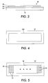
- FIG. 3 is a schematic elevational view of an embodiment of an ink jet printhead assembly.
- FIG. 4 is a schematic plan view of an embodiment of a diaphragm layer of the ink jet printhead assembly of FIG. 3.
- FIG. 5 is a schematic plan view of an embodiment of a thin film interconnect circuit of the ink jet printhead assembly of FIG. 3.
- FIG. 6 is a schematic elevational sectional view of a portion of an embodiment of a thin film interconnect circuit of the ink jet printhead assembly.
- FIG. 7 is a schematic elevational sectional view of a portion of another embodiment of a thin film interconnect circuit of the ink jet printhead assembly.
- FIG. 8 is a schematic elevational sectional view of a portion of a further embodiment of a thin film interconnect circuit of the ink jet printhead assembly.
- FIG. 9 is a schematic elevational sectional view of a portion of an embodiment of a thin film interconnect circuit of the ink jet printhead assembly.
- FIG. 10 is a schematic elevational sectional view of a portion of another embodiment of a thin film interconnect circuit of the ink jet printhead assembly.
- FIG. 1 is a schematic block diagram of an embodiment of a drop-on-demand printing apparatus that includes a controller 10 and a printhead assembly 20 that can include a plurality of drop emitting drop generators.
- the controller 10 selectively energizes the drop generators by providing a respective drive signal to each drop generator.
- Each of the drop generators can employ a piezoelectric transducer such as a ceramic piezoelectric transducer.
- each of the drop generators can employ a shear-mode transducer, an annular constrictive transducer, an electrostrictive transducer, an electromagnetic transducer, or a magnetorestrictive transducer.
- the printhead assembly 20 can be formed of a stack of laminated sheets or plates, such as of stainless steel.
- FIG. 2 is a schematic block diagram of an embodiment of a drop generator 30 that can be employed in the printhead assembly 20 of the printing apparatus shown in FIG. 1.
- the drop generator 30 includes an inlet channel 31 that receives ink 33 from a manifold, reservoir or other ink containing structure.
- the ink 33 flows into a pressure or pump chamber 35 that is bounded on one side, for example, by a flexible diaphragm 37.
- a thin-film interconnect structure 38 is attached to the flexible diaphragm, for example so as to overlie the pressure chamber 35.
- An electromechanical transducer 39 is attached to the thin film interconnect structure 38.
- the electromechanical transducer 39 can be a piezoelectric transducer that includes a piezo element 41 disposed for example between electrodes 42 and 43 that receive drop firing and non-firing signals from the controller 10 via the thin-film interconnect structure 38, for example.
- the electrode 43 is connected to ground in common with the controller 10, while the electrode 42 is actively driven to actuate the electromechanical transducer 41 through the interconnect structure 38.
- Actuation of the electromechanical transducer 39 causes ink to flow from the pressure chamber 35 to a drop forming outlet channel 45, from which an ink drop 49 is emitted toward a receiver medium 48 that can be a transfer surface, for example.
- the outlet channel 45 can include a nozzle or orifice 47.
- the ink 33 can be melted or phase changed solid ink, and the electromechanical transducer 39 can be a piezoelectric transducer that is operated in a bending mode, for example.
- FIG. 3 is a schematic elevational view of an embodiment of an ink jet printhead assembly 20 that can implement a plurality of drop generators 30 (FIG. 2), for example as an array of drop generators.
- the ink jet printhead assembly includes a fluid channel layer or substructure 131, a diaphragm layer 137 attached to the fluid channel layer 131, a thin-film interconnect circuit layer 138 disposed on the diaphragm layer 137 and a transducer layer 139 attached to the thin-film interconnect circuit layer 138.
- the fluid channel layer 131 implements the fluid channels and chambers of the drop generators 30, while the diaphragm layer 137 implements the diaphragms 37 of the drop generators.
- the thin-film interconnect circuit layer 138 implements the interconnect circuits 38, while the transducer layer 139 implements the electromechanical transducers 39 of the drop generators 30.
- the diaphragm layer 137 comprises a metal plate or sheet such as stainless steel that is attached or bonded to the fluid channel layer 131.
- the diaphragm layer 137 can also comprise an electrically non-conductive material such as a ceramic.
- the fluid channel layer 131 can comprise multiple laminated plates or sheets.
- the transducer layer 139 can comprise an array of kerfed ceramic transducers that are attached or bonded to the thin film interconnect circuit layer 138 by a suitable adhesive.
- asperity contacts are more particularly formed between the transducer layer 139 and the thin film interconnect layer 138, and the adhesive can comprise a low conductivity adhesive.
- an epoxy, acrylic, or phenolic adhesive can be used..
- FIG. 4 is a schematic plan view of an embodiment of a diaphragm layer 137 that includes a roughened, non-smooth bonding region 137A formed by particle blasting such as sand blasting, or by laser roughening, for example.
- the bonding region 137A can have a roughness average (Ra) in the range of about 1 microinch to about 100 microinches, for example.
- the bonding region 137A can have a roughness average in the range of about 5 microinches to about 20 microinches.
- the bonding region 137A can have a roughness average in the range of about 50 microinches to about 100 microinches.
- FIG. 5 is a schematic plan view of an embodiment of a thin film interconnect circuit layer 138 that includes conformal raised contact pads or regions 191 disposed over the roughened bonding region 137A (FIG. 4) of the diaphragm layer 137, wherein top surfaces of the raised contact regions 191 have a roughness that generally conforms to the roughness of the underlying roughened bonding region 137A of the diaphragm layer 137.
- the electromechanical transducers 39 (FIGS. 6-10) are attached to respective conformal raised contact pads 191 by a thin layer of adhesive, and asperity contacts are formed between the top surfaces of the raised contact portions 191 and the electromechanical transducers 39. As disclosed in various embodiments illustrated in FIGS.
- the conformal raised contact regions 191 can be formed by a thin film structure that can include for example a mesa layer and a patterned conductive layer.
- the layers of the thin film stack that form the conformal raised contact regions 191 are preferably conformal such that the top surfaces of the raised contact regions 191 have a roughness that generally conforms to the roughness of the underlying roughened bonding region 137A of the diaphragm layer 137.
- the top surfaces of the conformal raised contact regions 191 have a roughness average (Ra) in the range of about 1 microinch to about 100 microinches, which can be achieved for example by configuring the roughened bonding region 137A to have a suitable roughness.
- the top surfaces of the conformal raised contact regions 191 can have a roughness average in the range of about 5 microinches to about 20 microinches. Still further, the top surfaces of the raised conformal contact regions 191 can have a roughness average in the range of about 30 microinches to about 80 microinches.
- the thin film interconnect circuit 138 can provide for electrical interconnection to the individual electromechanical transducers 39.
- FIG. 6 is a schematic elevational sectional view of a portion of an embodiment of a thin film interconnect circuit layer 138 that can be used with an electrically conductive or non-conductive diaphragm layer 137.
- the thin film interconnect circuit layer 138 includes a conformal mesa layer 211 comprising a plurality of mesas, a conformal blanket dielectric layer 213 overlying the mesa layer 211 and the diaphragm layer 137, and a patterned conformal conductive layer 215 disposed on the blanket dielectric layer 213.
- the blanket dielectric layer serves to electrically isolate the diaphragm layer 137 from the patterned conformal conductive layer 215.
- the mesa layer 211 can be electrically non-conductive (e.g., dielectric) or conductive (e.g., metal).
- the mesas and the overlying portions of the conformal blanket dielectric layer 213 and the patterned conformal conductive layer 215 form raised contact regions or pads 191.
- the thin film interconnect circuit layer 138 can further include a patterned dielectric layer 217 having openings 217A through which the raised contact pads 191 extend.
- the raised contact pads 191 are higher than the other layers of the thin film interconnect circuit layer 138, and comprise the highest portions of the interconnect layer 138. This facilitates the attachment of an electromechanical transducer 39 to each of the raised contact pads 191.
- the conformal mesa layer 211 can comprise a suitably patterned conformal dielectric layer or conformal metal layer, for example.
- the patterned conformal conductive layer 215 can comprise a patterned conformal metal layer.
- the top surfaces of the raised contact pads 191 have a roughness that generally conforms to the roughened surface of the bonding region 137A of the metal diaphragm 137.
- the top surfaces of the raised contact pads 191 comprise roughened surfaces.
- the electromechanical transducers 39 are attached to respective contact pads 191 by a thin adhesive layer 221 that is sufficiently thin such that asperity contacts are formed between the top surface of the contact pads and the electromechanical transducers 39. Asperity contacts are more particularly formed by high points of the contact pads 191 that pass through the thin adhesive layer and contact the electromechanical transducers 39.
- FIG. 7 is a schematic elevational sectional view of a portion of a further embodiment of a thin film interconnect circuit layer 138 that can be used with an electrically conductive or non-conductive diaphragm layer 137.
- the thin film interconnect circuit layer 138 includes a conformal blanket dielectric layer 213, a conformal patterned conductive layer 215 disposed on the conformal blanket dielectric layer 213, and a conformal conductive mesa layer 211 comprising a plurality of conductive mesas overlying the patterned conformal conductive layer 215.
- the conductive mesas and the underlying portions of the conformal conductive layer 215 form raised contact regions or pads 191.
- the interconnect circuit layer 138 can further include a patterned dielectric layer 217 having openings 217A through which the raised contact pads 191 extend.
- the raised contact pads 191 are higher than the other layers of the interconnect circuit layer 138, and comprise the highest portions of the interconnect circuit layer 138. This facilitates the attachment of an electromechanical transducer 39 to each of the raised contact pads 191.
- the patterned conformal mesa layer 211 can comprise a suitably patterned conformal metal layer
- the patterned conformal conductive layer 215 can also comprise a suitably patterned conformal metal layer, for example.
- the top surfaces of the raised contact pads 191 have a roughness that generally conforms to the roughened surface of the bonding region 137A of the metal diaphragm 137.
- the electromechanical transducers 39 are attached to respective contact pads 191 by a thin adhesive layer 221 that is sufficiently thin such that asperity contacts are formed between the top surfaces of the raised contact pads 191 and the electromechanical transducers 39.
- FIG. 8 is a schematic elevational sectional view of a portion of a further embodiment of a thin film interconnect circuit layer 138 that can be used with an electrically conductive or non-conductive diaphragm 137.
- the interconnect circuit layer 138 includes a conformal blanket dielectric layer 213, a mesa layer 211 comprising a plurality of mesas overlying the conformal blanket dielectric layer 213, and a conformal patterned conductive layer 215 overlying the mesa layer 211.
- the mesa layer 211 can be electrically non-conductive (e.g., dielectric) or conductive (e.g., metal).
- the mesas and the overlying portions of the patterned conformal conductive layer 215 form raised contact regions or pads 191.
- the thin film interconnect circuit layer 138 can further include a patterned dielectric layer 217 having openings 217A through which the raised contact pads 191 extend.
- the raised contact pads 191 are higher than the other layers of the interconnect circuit layer 138, and comprise the highest portions of the interconnect layer 138. This facilitates the attachment of an electromechanical transducer 39 to each of the raised contact pads 191.
- the conformal mesa layer 211 can comprise a suitably patterned conformal dielectric layer or conformal metal layer, for example.
- the patterned conformal conductive layer 215 can comprise a patterned conformal metal layer.
- the top surfaces of the raised contact pads 191 have a roughness that generally conforms to the roughened surface of the bonding region 137A of the metal diaphragm 137.
- the electromechanical transducers 39 are attached to respective contact pads 191 by a thin adhesive layer 221 that is sufficiently thin such that asperity contacts are formed between the top surfaces of the raised contact pads 191 and the electromechanical transducers 39.
- FIG. 9 is a schematic elevational sectional view of a portion of an embodiment of a thin film interconnect circuit layer 138 that can be used with an electrically non-conductive diaphragm 137.
- the thin film interconnect circuit layer 138 includes a conformal mesa layer 211 comprising a plurality of mesas disposed on the bonding region 137A of the electrically non-conductive diaphragm 137, and a patterned conformal conductive layer 215 overlying the mesa layer 211.
- the mesa layer 211 can be electrically non-conductive (e.g., dielectric) or conductive (e.g., metal).
- the mesas and the overlying portions of the patterned conformal conductive layer 215 form raised contact regions or pads 191.
- the thin film interconnect circuit layer 138 can further include a patterned dielectric layer 217 having openings 217A through which the raised contact pads 191 extend.
- the raised contact pads 191 are higher than the other layers of the interconnect layer 138, and comprise the highest portions of the interconnect layer 138. This facilitates the attachment of an electromechanical transducer 39 to each of the raised contact pads 191.
- the conformal mesa layer 211 can comprise a suitably patterned conformal dielectric layer or patterned conformal metal layer, for example.
- the patterned conformal conductive layer 215 can comprise a patterned conformal metal layer, for example.
- the top surfaces of the raised contact pads 191 have a roughness that generally conforms to the roughened surface of the bonding region 137A of the metal diaphragm 137.
- the electromechanical transducers 39 are attached to respective contact pads 191 by a thin adhesive layer 221 that is sufficiently thin such that asperity contacts are formed between the top surfaces of the raised contact pads 191 and the electromechanical transducers 39.
- FIG. 10 is a schematic elevational sectional view of a portion of a further embodiment of a thin film interconnect circuit layer 138 that can be used with an electrically non-conductive diaphragm layer 137.
- the thin film interconnect circuit layer 138 includes a patterned conformal conductive layer 215 and a conductive mesa layer 211 comprising a plurality of mesas overlying the patterned conformal conductive layer 215.
- the conductive mesas and the underlying portions of the patterned conformal conductive layer 215 form raised contact regions or pads 191.
- the thin film interconnect circuit layer 138 can further include a patterned dielectric layer 217 having openings 217A through which the raised contact pads 191 extend.
- the raised contact pads 191 are higher than the other layers of the thin film interconnect circuit layer 138, and comprise the highest portions of the interconnect layer 138. This facilitates the attachment of an electromechanical transducer 39 to each of the raised contact pads 191.
- the patterned conformal conductive mesa layer 211 can comprise a suitably patterned conformal metal layer, and the patterned conformal conductive layer 215 can also comprise a suitably patterned conformal metal layer, for example.
- the top surfaces of the raised contact pads 191 have a roughness that generally conforms to the roughened surface of the bonding region 137A of the metal diaphragm 137.
- the electromechanical transducers 39 are attached to respective contact pads 191 by a thin adhesive layer 221 that is sufficiently thin such that asperity contacts are formed between the top surfaces of the raised contact pads 191 and the electromechanical transducers 39.
- Each dielectric layer of the thin film interconnect circuit layer 138 can comprise silicon oxide, silicon nitride, or silicon oxynitride, for example, and can have a thickness in the range of about 0.1 micrometers of about 5 micrometers. More specifically, each dielectric layer can have a thickness in the range of about 1 micrometers to about 2 micrometers.
- Each conductive layer of the thin film interconnect circuit layer 138 can comprise aluminum, chromium, nickel, tantalum or copper, for example, and can have a thickness in the range of about 0.1 micrometers of about 5 micrometers. More specifically, each conductive layer can have a thickness in the range of about 1 micrometers to about 2 micrometers.
Landscapes
- Particle Formation And Scattering Control In Inkjet Printers (AREA)
- Micromachines (AREA)
Abstract
Description
- The subject disclosure is generally directed to drop emitting apparatus, and more particularly to ink jet apparatus.
- Drop on demand ink jet technology for producing printed media has been employed in commercial products such as printers, plotters, and facsimile machines. Generally, an ink jet image is formed by selective placement on a receiver surface of ink drops emitted by a plurality of drop generators implemented in a printhead or a printhead assembly. For example, the printhead assembly and the receiver surface are caused to move relative to each other, and drop generators are controlled to emit drops at appropriate times, for example by an appropriate controller. The receiver surface can be a transfer surface or a print medium such as paper. In the case of a transfer surface, the image printed thereon is subsequently transferred to an output print medium such as paper.
- A known ink jet printhead structure employs electromechanical transducers that are attached to a metal diaphragm plate, and it can be difficult to make electrical connections to the electromechanical transducers.
In view of these problems the present invention provides a drop emitting apparatus and a drop generator as defined inclaims 1, 9 and 10.
In further embodiments of these apparatuses, the raised contact areas include conformal conductive mesas.
In a further embodiment the thin film circuit comprises a conformal mesa layer and a patterned conformal conductive layer overlying the conformal mesa layer.
In a further embodiment the thin film circuit comprises blanket conformal dielectric layer, a conformal mesa layer overlying the blanket conformal dielectric layer, and a patterned conformal conductive layer overlying the conformal mesa layer.
In a further embodiment the thin film circuit comprises a conformal mesa layer, a blanket dielectric conformal layer overlying the conformal mesa layer, and a patterned conformal conductive layer overlying the blanket conformal dielectric layer.
In a further embodiment the thin film circuit comprises a patterned conformal conductive layer and a conformal conductive mesa layer overlying the patterned conformal conductive layer.
In a further embodiment the thin film circuit comprises a blanket conformal dielectric layer, a patterned conformal conductive layer overlying the blanket conformal dielectric layer, and a conformal conductive mesa layer overlying the patterned conformal conductive layer.
In a further embodiment the roughened bonding region comprises a particle blasted region.
In a further embodiment the roughened bonding region comprises a laser roughened region.
In a further embodiment the fluid channel layer receives melted solid ink.
In a further embodiment the electromechanical transducers comprise piezoelectric transducers.
In a further embodiment the fluid channel layer comprises a stack of patterned metal plates.
Moreover, a method of making a drop emitting apparatus comprises: - roughening a region of a surface of a diaphragm layer;
- forming on the roughened region a thin film circuit having conformal raised contact regions; and
- adhesively attaching piezoelectric transducers to the conformal raised contact regions and forming asperity contacts between the conformal raised contact regions and the piezoelectric transducers.
-
- FIG. 1 is a schematic block diagram of an embodiment of a drop-on-demand drop emitting apparatus.
- FIG. 2 is a schematic block diagram of an embodiment of a drop generator that can be employed in the drop emitting apparatus of FIG. 1.
- FIG. 3 is a schematic elevational view of an embodiment of an ink jet printhead assembly.
- FIG. 4 is a schematic plan view of an embodiment of a diaphragm layer of the ink jet printhead assembly of FIG. 3.
- FIG. 5 is a schematic plan view of an embodiment of a thin film interconnect circuit of the ink jet printhead assembly of FIG. 3.
- FIG. 6 is a schematic elevational sectional view of a portion of an embodiment of a thin film interconnect circuit of the ink jet printhead assembly.
- FIG. 7 is a schematic elevational sectional view of a portion of another embodiment of a thin film interconnect circuit of the ink jet printhead assembly.
- FIG. 8 is a schematic elevational sectional view of a portion of a further embodiment of a thin film interconnect circuit of the ink jet printhead assembly.
- FIG. 9 is a schematic elevational sectional view of a portion of an embodiment of a thin film interconnect circuit of the ink jet printhead assembly.
- FIG. 10 is a schematic elevational sectional view of a portion of another embodiment of a thin film interconnect circuit of the ink jet printhead assembly.
- FIG. 1 is a schematic block diagram of an embodiment of a drop-on-demand printing apparatus that includes a
controller 10 and aprinthead assembly 20 that can include a plurality of drop emitting drop generators. Thecontroller 10 selectively energizes the drop generators by providing a respective drive signal to each drop generator. Each of the drop generators can employ a piezoelectric transducer such as a ceramic piezoelectric transducer. As other examples, each of the drop generators can employ a shear-mode transducer, an annular constrictive transducer, an electrostrictive transducer, an electromagnetic transducer, or a magnetorestrictive transducer. Theprinthead assembly 20 can be formed of a stack of laminated sheets or plates, such as of stainless steel. - FIG. 2 is a schematic block diagram of an embodiment of a
drop generator 30 that can be employed in theprinthead assembly 20 of the printing apparatus shown in FIG. 1. Thedrop generator 30 includes aninlet channel 31 that receivesink 33 from a manifold, reservoir or other ink containing structure. Theink 33 flows into a pressure orpump chamber 35 that is bounded on one side, for example, by aflexible diaphragm 37. A thin-film interconnect structure 38 is attached to the flexible diaphragm, for example so as to overlie thepressure chamber 35. Anelectromechanical transducer 39 is attached to the thinfilm interconnect structure 38. Theelectromechanical transducer 39 can be a piezoelectric transducer that includes apiezo element 41 disposed for example betweenelectrodes controller 10 via the thin-film interconnect structure 38, for example. Theelectrode 43 is connected to ground in common with thecontroller 10, while theelectrode 42 is actively driven to actuate theelectromechanical transducer 41 through theinterconnect structure 38. Actuation of theelectromechanical transducer 39 causes ink to flow from thepressure chamber 35 to a drop formingoutlet channel 45, from which anink drop 49 is emitted toward areceiver medium 48 that can be a transfer surface, for example. Theoutlet channel 45 can include a nozzle ororifice 47. - The
ink 33 can be melted or phase changed solid ink, and theelectromechanical transducer 39 can be a piezoelectric transducer that is operated in a bending mode, for example. - FIG. 3 is a schematic elevational view of an embodiment of an ink
jet printhead assembly 20 that can implement a plurality of drop generators 30 (FIG. 2), for example as an array of drop generators. The ink jet printhead assembly includes a fluid channel layer orsubstructure 131, adiaphragm layer 137 attached to thefluid channel layer 131, a thin-filminterconnect circuit layer 138 disposed on thediaphragm layer 137 and atransducer layer 139 attached to the thin-filminterconnect circuit layer 138. Thefluid channel layer 131 implements the fluid channels and chambers of thedrop generators 30, while thediaphragm layer 137 implements thediaphragms 37 of the drop generators. The thin-filminterconnect circuit layer 138 implements theinterconnect circuits 38, while thetransducer layer 139 implements theelectromechanical transducers 39 of thedrop generators 30. - By way of illustrative example, the
diaphragm layer 137 comprises a metal plate or sheet such as stainless steel that is attached or bonded to thefluid channel layer 131. Thediaphragm layer 137 can also comprise an electrically non-conductive material such as a ceramic. Also by way of illustrative example, thefluid channel layer 131 can comprise multiple laminated plates or sheets. Thetransducer layer 139 can comprise an array of kerfed ceramic transducers that are attached or bonded to the thin filminterconnect circuit layer 138 by a suitable adhesive. As described further herein, asperity contacts are more particularly formed between thetransducer layer 139 and the thinfilm interconnect layer 138, and the adhesive can comprise a low conductivity adhesive. For example, an epoxy, acrylic, or phenolic adhesive can be used.. - FIG. 4 is a schematic plan view of an embodiment of a
diaphragm layer 137 that includes a roughened, non-smoothbonding region 137A formed by particle blasting such as sand blasting, or by laser roughening, for example. Thebonding region 137A can have a roughness average (Ra) in the range of about 1 microinch to about 100 microinches, for example. As another example, thebonding region 137A can have a roughness average in the range of about 5 microinches to about 20 microinches. Still further, thebonding region 137A can have a roughness average in the range of about 50 microinches to about 100 microinches. - FIG. 5 is a schematic plan view of an embodiment of a thin film
interconnect circuit layer 138 that includes conformal raised contact pads orregions 191 disposed over the roughenedbonding region 137A (FIG. 4) of thediaphragm layer 137, wherein top surfaces of the raisedcontact regions 191 have a roughness that generally conforms to the roughness of the underlying roughenedbonding region 137A of thediaphragm layer 137. The electromechanical transducers 39 (FIGS. 6-10) are attached to respective conformal raisedcontact pads 191 by a thin layer of adhesive, and asperity contacts are formed between the top surfaces of the raisedcontact portions 191 and theelectromechanical transducers 39. As disclosed in various embodiments illustrated in FIGS. 6-10, the conformal raisedcontact regions 191 can be formed by a thin film structure that can include for example a mesa layer and a patterned conductive layer. The layers of the thin film stack that form the conformal raisedcontact regions 191 are preferably conformal such that the top surfaces of the raisedcontact regions 191 have a roughness that generally conforms to the roughness of the underlying roughenedbonding region 137A of thediaphragm layer 137. By way of illustrative example, the top surfaces of the conformal raisedcontact regions 191 have a roughness average (Ra) in the range of about 1 microinch to about 100 microinches, which can be achieved for example by configuring the roughenedbonding region 137A to have a suitable roughness. As another example, the top surfaces of the conformal raisedcontact regions 191 can have a roughness average in the range of about 5 microinches to about 20 microinches. Still further, the top surfaces of the raisedconformal contact regions 191 can have a roughness average in the range of about 30 microinches to about 80 microinches. The thinfilm interconnect circuit 138 can provide for electrical interconnection to the individualelectromechanical transducers 39. - FIG. 6 is a schematic elevational sectional view of a portion of an embodiment of a thin film
interconnect circuit layer 138 that can be used with an electrically conductive ornon-conductive diaphragm layer 137. The thin filminterconnect circuit layer 138 includes aconformal mesa layer 211 comprising a plurality of mesas, a conformal blanket dielectric layer 213 overlying themesa layer 211 and thediaphragm layer 137, and a patterned conformalconductive layer 215 disposed on the blanket dielectric layer 213. The blanket dielectric layer serves to electrically isolate thediaphragm layer 137 from the patterned conformalconductive layer 215. Themesa layer 211 can be electrically non-conductive (e.g., dielectric) or conductive (e.g., metal). The mesas and the overlying portions of the conformal blanket dielectric layer 213 and the patterned conformalconductive layer 215 form raised contact regions orpads 191. The thin filminterconnect circuit layer 138 can further include a patterneddielectric layer 217 havingopenings 217A through which the raisedcontact pads 191 extend. The raisedcontact pads 191 are higher than the other layers of the thin filminterconnect circuit layer 138, and comprise the highest portions of theinterconnect layer 138. This facilitates the attachment of anelectromechanical transducer 39 to each of the raisedcontact pads 191. - In the embodiment of a thin film interconnect circuit schematically depicted in FIG. 6, the
conformal mesa layer 211 can comprise a suitably patterned conformal dielectric layer or conformal metal layer, for example. The patterned conformalconductive layer 215 can comprise a patterned conformal metal layer. - Since the
mesa layer 211, the blanket dielectric layer 213 and the patternedconductive layer 215 are conformal layers, the top surfaces of the raisedcontact pads 191 have a roughness that generally conforms to the roughened surface of thebonding region 137A of themetal diaphragm 137. In other words, the top surfaces of the raisedcontact pads 191 comprise roughened surfaces. Theelectromechanical transducers 39 are attached torespective contact pads 191 by a thinadhesive layer 221 that is sufficiently thin such that asperity contacts are formed between the top surface of the contact pads and theelectromechanical transducers 39. Asperity contacts are more particularly formed by high points of thecontact pads 191 that pass through the thin adhesive layer and contact theelectromechanical transducers 39. - FIG. 7 is a schematic elevational sectional view of a portion of a further embodiment of a thin film
interconnect circuit layer 138 that can be used with an electrically conductive ornon-conductive diaphragm layer 137. The thin filminterconnect circuit layer 138 includes a conformal blanket dielectric layer 213, a conformal patternedconductive layer 215 disposed on the conformal blanket dielectric layer 213, and a conformalconductive mesa layer 211 comprising a plurality of conductive mesas overlying the patterned conformalconductive layer 215. The conductive mesas and the underlying portions of the conformalconductive layer 215 form raised contact regions orpads 191. Theinterconnect circuit layer 138 can further include a patterneddielectric layer 217 havingopenings 217A through which the raisedcontact pads 191 extend. The raisedcontact pads 191 are higher than the other layers of theinterconnect circuit layer 138, and comprise the highest portions of theinterconnect circuit layer 138. This facilitates the attachment of anelectromechanical transducer 39 to each of the raisedcontact pads 191. - In the embodiment schematically depicted in FIG. 7, the patterned
conformal mesa layer 211 can comprise a suitably patterned conformal metal layer, and the patterned conformalconductive layer 215 can also comprise a suitably patterned conformal metal layer, for example. - Since the blanket dielectric layer 213, the patterned
conductive layer 215, and themesa layer 211 are conformal layers, the top surfaces of the raisedcontact pads 191 have a roughness that generally conforms to the roughened surface of thebonding region 137A of themetal diaphragm 137. Theelectromechanical transducers 39 are attached torespective contact pads 191 by a thinadhesive layer 221 that is sufficiently thin such that asperity contacts are formed between the top surfaces of the raisedcontact pads 191 and theelectromechanical transducers 39. - FIG. 8 is a schematic elevational sectional view of a portion of a further embodiment of a thin film
interconnect circuit layer 138 that can be used with an electrically conductive ornon-conductive diaphragm 137. Theinterconnect circuit layer 138 includes a conformal blanket dielectric layer 213, amesa layer 211 comprising a plurality of mesas overlying the conformal blanket dielectric layer 213, and a conformal patternedconductive layer 215 overlying themesa layer 211. Themesa layer 211 can be electrically non-conductive (e.g., dielectric) or conductive (e.g., metal). The mesas and the overlying portions of the patterned conformalconductive layer 215 form raised contact regions orpads 191. The thin filminterconnect circuit layer 138 can further include a patterneddielectric layer 217 havingopenings 217A through which the raisedcontact pads 191 extend. The raisedcontact pads 191 are higher than the other layers of theinterconnect circuit layer 138, and comprise the highest portions of theinterconnect layer 138. This facilitates the attachment of anelectromechanical transducer 39 to each of the raisedcontact pads 191. - In the embodiment schematically depicted in FIG. 8, the
conformal mesa layer 211 can comprise a suitably patterned conformal dielectric layer or conformal metal layer, for example. The patterned conformalconductive layer 215 can comprise a patterned conformal metal layer. - Since the blanket dielectric layer 213, the
mesa layer 211, and the patternedconductive layer 215 are conformal layers, the top surfaces of the raisedcontact pads 191 have a roughness that generally conforms to the roughened surface of thebonding region 137A of themetal diaphragm 137. Theelectromechanical transducers 39 are attached torespective contact pads 191 by a thinadhesive layer 221 that is sufficiently thin such that asperity contacts are formed between the top surfaces of the raisedcontact pads 191 and theelectromechanical transducers 39. - FIG. 9 is a schematic elevational sectional view of a portion of an embodiment of a thin film
interconnect circuit layer 138 that can be used with an electricallynon-conductive diaphragm 137. The thin filminterconnect circuit layer 138 includes aconformal mesa layer 211 comprising a plurality of mesas disposed on thebonding region 137A of the electricallynon-conductive diaphragm 137, and a patterned conformalconductive layer 215 overlying themesa layer 211. Themesa layer 211 can be electrically non-conductive (e.g., dielectric) or conductive (e.g., metal). The mesas and the overlying portions of the patterned conformalconductive layer 215 form raised contact regions orpads 191. The thin filminterconnect circuit layer 138 can further include a patterneddielectric layer 217 havingopenings 217A through which the raisedcontact pads 191 extend. The raisedcontact pads 191 are higher than the other layers of theinterconnect layer 138, and comprise the highest portions of theinterconnect layer 138. This facilitates the attachment of anelectromechanical transducer 39 to each of the raisedcontact pads 191. - In the embodiment schematically depicted in FIG. 9, the
conformal mesa layer 211 can comprise a suitably patterned conformal dielectric layer or patterned conformal metal layer, for example. The patterned conformalconductive layer 215 can comprise a patterned conformal metal layer, for example. - Since the
mesa layer 211 and the patternedconductive layer 215 are conformal layers, the top surfaces of the raisedcontact pads 191 have a roughness that generally conforms to the roughened surface of thebonding region 137A of themetal diaphragm 137. Theelectromechanical transducers 39 are attached torespective contact pads 191 by a thinadhesive layer 221 that is sufficiently thin such that asperity contacts are formed between the top surfaces of the raisedcontact pads 191 and theelectromechanical transducers 39. - FIG. 10 is a schematic elevational sectional view of a portion of a further embodiment of a thin film
interconnect circuit layer 138 that can be used with an electricallynon-conductive diaphragm layer 137. The thin filminterconnect circuit layer 138 includes a patterned conformalconductive layer 215 and aconductive mesa layer 211 comprising a plurality of mesas overlying the patterned conformalconductive layer 215. The conductive mesas and the underlying portions of the patterned conformalconductive layer 215 form raised contact regions orpads 191. The thin filminterconnect circuit layer 138 can further include a patterneddielectric layer 217 havingopenings 217A through which the raisedcontact pads 191 extend. The raisedcontact pads 191 are higher than the other layers of the thin filminterconnect circuit layer 138, and comprise the highest portions of theinterconnect layer 138. This facilitates the attachment of anelectromechanical transducer 39 to each of the raisedcontact pads 191. - In the embodiment schematically depicted in FIG. 10, the patterned conformal
conductive mesa layer 211 can comprise a suitably patterned conformal metal layer, and the patterned conformalconductive layer 215 can also comprise a suitably patterned conformal metal layer, for example. - Since the patterned
conductive layer 215 and theconductive mesa layer 211 are conformal layers, the top surfaces of the raisedcontact pads 191 have a roughness that generally conforms to the roughened surface of thebonding region 137A of themetal diaphragm 137. Theelectromechanical transducers 39 are attached torespective contact pads 191 by a thinadhesive layer 221 that is sufficiently thin such that asperity contacts are formed between the top surfaces of the raisedcontact pads 191 and theelectromechanical transducers 39. - Each dielectric layer of the thin film
interconnect circuit layer 138 can comprise silicon oxide, silicon nitride, or silicon oxynitride, for example, and can have a thickness in the range of about 0.1 micrometers of about 5 micrometers. More specifically, each dielectric layer can have a thickness in the range of about 1 micrometers to about 2 micrometers. - Each conductive layer of the thin film
interconnect circuit layer 138 can comprise aluminum, chromium, nickel, tantalum or copper, for example, and can have a thickness in the range of about 0.1 micrometers of about 5 micrometers. More specifically, each conductive layer can have a thickness in the range of about 1 micrometers to about 2 micrometers.
Claims (10)
- A drop emitting apparatus comprising:a fluid channel layer;a diaphragm layer disposed on the fluid channel layer;a roughened bonding region formed on a surface of the diaphragm layer;a thin film circuit having conformal raised contact regions disposed on the roughened bonding region; anda plurality of electromechanical transducers adhesively attached to the conformal raised contact regions and electrically connected to the conformal raised contact regions by asperity contacts formed between the conformal raised contact regions and the electromechanical transducers.
- The drop emitting apparatus of claim 1 wherein the roughened bonding region has a roughness average in the range of about 1 microinch to about 100 microinches.
- The drop emitting apparatus of claim 1 wherein the roughened bonding region has a roughness average in the range of about 5 microinches to about 20 microinches.
- The drop emitting apparatus of claim 1 wherein the roughened bonding region has a roughness average in the range of about 30 microinches to about 80 microinches.
- The drop emitting apparatus of claim 1 wherein the raised contact regions have a top surface roughness average in the range of about 1 microinch to about 100 microinches.
- The drop emitting apparatus of claim 1 wherein the raised contact regions have a top surface roughness average in the range of about 5 microinches to about 20 microinches.
- The drop emitting apparatus of claim 1 wherein the raised contact regions have a top surface roughness average in the range of about 30 microinches to about 80 microinches.
- The drop emitting apparatus of claim 1 wherein the raised contact areas include conformal dielectric mesas.
- A drop emitting apparatus comprising:wherein the conformal raised contact regions include conformal mesas; anda fluid channel layer;a metal diaphragm layer attached to the fluid channel layer;a roughened bonding region formed on a surface of the metal diaphragm layer;a thin film circuit having conformal raised contact regions disposed on the roughened bonding region;
a plurality of piezoelectric transducers adhesively attached to the conformal raised contact regions and electrically connected to the conformal raised contact regions by asperity contacts formed between the conformal raised contact regions and the piezoelectric transducers. - A drop generator comprising:a pressure chamber;a metal diaphragm forming a wall of the pressure chamber, the metal diaphragm including a roughened bonding surface;a thin film conformal raised contact region disposed on the roughened bonding surface;a piezoelectric transducer adhesively attached to the conformal raised contact region and electrically connected to the conformal raised contact region by asperity contacts formed between the conformal raised contact region and the piezoelectric transducer;an outlet channel connected to the pressure chamber; anda drop emitting nozzle disposed at an end of the outlet channel.
Applications Claiming Priority (2)
| Application Number | Priority Date | Filing Date | Title |
|---|---|---|---|
| US702247 | 2003-11-05 | ||
| US10/702,247 US7048361B2 (en) | 2003-11-05 | 2003-11-05 | Ink jet apparatus |
Publications (2)
| Publication Number | Publication Date |
|---|---|
| EP1529642A1 true EP1529642A1 (en) | 2005-05-11 |
| EP1529642B1 EP1529642B1 (en) | 2006-10-18 |
Family
ID=34435546
Family Applications (1)
| Application Number | Title | Priority Date | Filing Date |
|---|---|---|---|
| EP04026226A Expired - Fee Related EP1529642B1 (en) | 2003-11-05 | 2004-11-04 | Ink jet apparatus |
Country Status (7)
| Country | Link |
|---|---|
| US (1) | US7048361B2 (en) |
| EP (1) | EP1529642B1 (en) |
| JP (1) | JP4597633B2 (en) |
| CN (1) | CN100415515C (en) |
| BR (1) | BRPI0404831A (en) |
| CA (1) | CA2486454C (en) |
| DE (1) | DE602004002827T2 (en) |
Families Citing this family (6)
| Publication number | Priority date | Publication date | Assignee | Title |
|---|---|---|---|---|
| CN102165574A (en) * | 2008-09-18 | 2011-08-24 | 富士胶卷迪马蒂克斯股份有限公司 | Bonding on silicon substrate having a groove |
| KR20100076083A (en) * | 2008-12-17 | 2010-07-06 | 서울반도체 주식회사 | Light emitting diode having plurality of light emitting cells and method of fabricating the same |
| US9070851B2 (en) | 2010-09-24 | 2015-06-30 | Seoul Semiconductor Co., Ltd. | Wafer-level light emitting diode package and method of fabricating the same |
| US9315021B2 (en) * | 2014-02-27 | 2016-04-19 | Xerox Corporation | Multiple thin film piezoelectric elements driving single jet ejection system |
| US9662880B2 (en) | 2015-09-11 | 2017-05-30 | Xerox Corporation | Integrated thin film piezoelectric printhead |
| CN205944139U (en) | 2016-03-30 | 2017-02-08 | 首尔伟傲世有限公司 | Ultraviolet ray light -emitting diode spare and contain this emitting diode module |
Citations (6)
| Publication number | Priority date | Publication date | Assignee | Title |
|---|---|---|---|---|
| US4516140A (en) * | 1983-12-27 | 1985-05-07 | At&T Teletype Corporation | Print head actuator for an ink jet printer |
| EP0629007A1 (en) * | 1993-06-08 | 1994-12-14 | Ngk Insulators, Ltd. | Piezoelectric device |
| US5394179A (en) * | 1992-03-20 | 1995-02-28 | Scitex Digital Printing, Inc. | Stimulator for continous ink print head |
| EP0887187A2 (en) * | 1997-06-25 | 1998-12-30 | NEC Corporation | Ink jet recording head and method of producing the same |
| US6019457A (en) * | 1991-01-30 | 2000-02-01 | Canon Information Systems Research Australia Pty Ltd. | Ink jet print device and print head or print apparatus using the same |
| US6532028B1 (en) * | 1996-06-26 | 2003-03-11 | Spectra, Inc. | Ink jet printer having a ceramic piezoelectric transducer |
Family Cites Families (7)
| Publication number | Priority date | Publication date | Assignee | Title |
|---|---|---|---|---|
| JPS5586765A (en) * | 1978-12-23 | 1980-06-30 | Seiko Epson Corp | Electric wiring for ink jet head |
| US4730197A (en) * | 1985-11-06 | 1988-03-08 | Pitney Bowes Inc. | Impulse ink jet system |
| US4680595A (en) * | 1985-11-06 | 1987-07-14 | Pitney Bowes Inc. | Impulse ink jet print head and method of making same |
| US4703333A (en) * | 1986-01-30 | 1987-10-27 | Pitney Bowes Inc. | Impulse ink jet print head with inclined and stacked arrays |
| US4695854A (en) * | 1986-07-30 | 1987-09-22 | Pitney Bowes Inc. | External manifold for ink jet array |
| JPH1034919A (en) * | 1996-07-23 | 1998-02-10 | Ricoh Co Ltd | Ink jet head |
| US6955419B2 (en) * | 2003-11-05 | 2005-10-18 | Xerox Corporation | Ink jet apparatus |
-
2003
- 2003-11-05 US US10/702,247 patent/US7048361B2/en active Active
-
2004
- 2004-11-01 JP JP2004317451A patent/JP4597633B2/en not_active Expired - Fee Related
- 2004-11-01 CA CA002486454A patent/CA2486454C/en not_active Expired - Fee Related
- 2004-11-04 EP EP04026226A patent/EP1529642B1/en not_active Expired - Fee Related
- 2004-11-04 DE DE602004002827T patent/DE602004002827T2/en active Active
- 2004-11-05 BR BR0404831-8A patent/BRPI0404831A/en not_active IP Right Cessation
- 2004-11-05 CN CNB2004100905931A patent/CN100415515C/en not_active Expired - Fee Related
Patent Citations (6)
| Publication number | Priority date | Publication date | Assignee | Title |
|---|---|---|---|---|
| US4516140A (en) * | 1983-12-27 | 1985-05-07 | At&T Teletype Corporation | Print head actuator for an ink jet printer |
| US6019457A (en) * | 1991-01-30 | 2000-02-01 | Canon Information Systems Research Australia Pty Ltd. | Ink jet print device and print head or print apparatus using the same |
| US5394179A (en) * | 1992-03-20 | 1995-02-28 | Scitex Digital Printing, Inc. | Stimulator for continous ink print head |
| EP0629007A1 (en) * | 1993-06-08 | 1994-12-14 | Ngk Insulators, Ltd. | Piezoelectric device |
| US6532028B1 (en) * | 1996-06-26 | 2003-03-11 | Spectra, Inc. | Ink jet printer having a ceramic piezoelectric transducer |
| EP0887187A2 (en) * | 1997-06-25 | 1998-12-30 | NEC Corporation | Ink jet recording head and method of producing the same |
Also Published As
| Publication number | Publication date |
|---|---|
| CA2486454A1 (en) | 2005-05-05 |
| DE602004002827D1 (en) | 2006-11-30 |
| CN100415515C (en) | 2008-09-03 |
| JP2005138586A (en) | 2005-06-02 |
| US7048361B2 (en) | 2006-05-23 |
| BRPI0404831A (en) | 2005-06-28 |
| JP4597633B2 (en) | 2010-12-15 |
| CN1613645A (en) | 2005-05-11 |
| EP1529642B1 (en) | 2006-10-18 |
| DE602004002827T2 (en) | 2007-02-01 |
| US20050093929A1 (en) | 2005-05-05 |
| CA2486454C (en) | 2008-04-15 |
Similar Documents
| Publication | Publication Date | Title |
|---|---|---|
| US8397359B2 (en) | Method of manufacturing a drop generator | |
| US6695437B2 (en) | Inkjet recording head and method for driving an inkjet recording head | |
| JP2015147374A (en) | Liquid ejection head and recording apparatus | |
| EP1795355A1 (en) | Drop generator | |
| EP1529641B1 (en) | Ink jet apparatus | |
| EP1529642B1 (en) | Ink jet apparatus | |
| JP4563786B2 (en) | Liquid ejecting apparatus and driving method thereof | |
| JP5934058B2 (en) | In situ flexible circuit embossing to form electrical interconnects | |
| US20050045272A1 (en) | Laser removal of adhesive | |
| EP1431035A1 (en) | Ink jet apparatus | |
| US7143488B2 (en) | Drop emitting apparatus | |
| US6296346B1 (en) | Apparatus for jetting ink utilizing lamb wave and method for manufacturing the same | |
| US7665828B2 (en) | Drop generator | |
| JP4392200B2 (en) | Print head and electronics | |
| JP2009051188A (en) | Liquid discharge device | |
| JP2001219557A (en) | Ink jet head and ink jet recorder | |
| JP2003025572A (en) | Piezoelectric actuator, its manufacturing method and ink jet printing head with the same | |
| JPH10264387A (en) | Ink-jet recording head and its manufacture |
Legal Events
| Date | Code | Title | Description |
|---|---|---|---|
| PUAI | Public reference made under article 153(3) epc to a published international application that has entered the european phase |
Free format text: ORIGINAL CODE: 0009012 |
|
| AK | Designated contracting states |
Kind code of ref document: A1 Designated state(s): AT BE BG CH CY CZ DE DK EE ES FI FR GB GR HU IE IS IT LI LU MC NL PL PT RO SE SI SK TR |
|
| AX | Request for extension of the european patent |
Extension state: AL HR LT LV MK YU |
|
| 17P | Request for examination filed |
Effective date: 20051111 |
|
| AKX | Designation fees paid |
Designated state(s): DE FR GB |
|
| GRAP | Despatch of communication of intention to grant a patent |
Free format text: ORIGINAL CODE: EPIDOSNIGR1 |
|
| GRAS | Grant fee paid |
Free format text: ORIGINAL CODE: EPIDOSNIGR3 |
|
| GRAA | (expected) grant |
Free format text: ORIGINAL CODE: 0009210 |
|
| AK | Designated contracting states |
Kind code of ref document: B1 Designated state(s): DE FR GB |
|
| REG | Reference to a national code |
Ref country code: GB Ref legal event code: FG4D |
|
| REF | Corresponds to: |
Ref document number: 602004002827 Country of ref document: DE Date of ref document: 20061130 Kind code of ref document: P |
|
| ET | Fr: translation filed | ||
| PLBE | No opposition filed within time limit |
Free format text: ORIGINAL CODE: 0009261 |
|
| STAA | Information on the status of an ep patent application or granted ep patent |
Free format text: STATUS: NO OPPOSITION FILED WITHIN TIME LIMIT |
|
| 26N | No opposition filed |
Effective date: 20070719 |
|
| REG | Reference to a national code |
Ref country code: FR Ref legal event code: PLFP Year of fee payment: 12 |
|
| REG | Reference to a national code |
Ref country code: FR Ref legal event code: PLFP Year of fee payment: 13 |
|
| PGFP | Annual fee paid to national office [announced via postgrant information from national office to epo] |
Ref country code: FR Payment date: 20161024 Year of fee payment: 13 Ref country code: DE Payment date: 20161020 Year of fee payment: 13 Ref country code: GB Payment date: 20161027 Year of fee payment: 13 |
|
| REG | Reference to a national code |
Ref country code: DE Ref legal event code: R119 Ref document number: 602004002827 Country of ref document: DE |
|
| GBPC | Gb: european patent ceased through non-payment of renewal fee |
Effective date: 20171104 |
|
| REG | Reference to a national code |
Ref country code: FR Ref legal event code: ST Effective date: 20180731 |
|
| PG25 | Lapsed in a contracting state [announced via postgrant information from national office to epo] |
Ref country code: DE Free format text: LAPSE BECAUSE OF NON-PAYMENT OF DUE FEES Effective date: 20180602 Ref country code: FR Free format text: LAPSE BECAUSE OF NON-PAYMENT OF DUE FEES Effective date: 20171130 |
|
| PG25 | Lapsed in a contracting state [announced via postgrant information from national office to epo] |
Ref country code: GB Free format text: LAPSE BECAUSE OF NON-PAYMENT OF DUE FEES Effective date: 20171104 |