EP1529641B1 - Ink jet apparatus - Google Patents
Ink jet apparatus Download PDFInfo
- Publication number
- EP1529641B1 EP1529641B1 EP04026225A EP04026225A EP1529641B1 EP 1529641 B1 EP1529641 B1 EP 1529641B1 EP 04026225 A EP04026225 A EP 04026225A EP 04026225 A EP04026225 A EP 04026225A EP 1529641 B1 EP1529641 B1 EP 1529641B1
- Authority
- EP
- European Patent Office
- Prior art keywords
- layer
- disposed
- diaphragm
- fluid channel
- emitting apparatus
- Prior art date
- Legal status (The legal status is an assumption and is not a legal conclusion. Google has not performed a legal analysis and makes no representation as to the accuracy of the status listed.)
- Expired - Fee Related
Links
Images

Classifications
-
- B—PERFORMING OPERATIONS; TRANSPORTING
- B41—PRINTING; LINING MACHINES; TYPEWRITERS; STAMPS
- B41J—TYPEWRITERS; SELECTIVE PRINTING MECHANISMS, i.e. MECHANISMS PRINTING OTHERWISE THAN FROM A FORME; CORRECTION OF TYPOGRAPHICAL ERRORS
- B41J2/00—Typewriters or selective printing mechanisms characterised by the printing or marking process for which they are designed
- B41J2/005—Typewriters or selective printing mechanisms characterised by the printing or marking process for which they are designed characterised by bringing liquid or particles selectively into contact with a printing material
- B41J2/01—Ink jet
- B41J2/135—Nozzles
- B41J2/14—Structure thereof only for on-demand ink jet heads
- B41J2/14201—Structure of print heads with piezoelectric elements
- B41J2/14233—Structure of print heads with piezoelectric elements of film type, deformed by bending and disposed on a diaphragm
-
- B—PERFORMING OPERATIONS; TRANSPORTING
- B41—PRINTING; LINING MACHINES; TYPEWRITERS; STAMPS
- B41J—TYPEWRITERS; SELECTIVE PRINTING MECHANISMS, i.e. MECHANISMS PRINTING OTHERWISE THAN FROM A FORME; CORRECTION OF TYPOGRAPHICAL ERRORS
- B41J2/00—Typewriters or selective printing mechanisms characterised by the printing or marking process for which they are designed
- B41J2/005—Typewriters or selective printing mechanisms characterised by the printing or marking process for which they are designed characterised by bringing liquid or particles selectively into contact with a printing material
- B41J2/01—Ink jet
- B41J2/135—Nozzles
- B41J2/14—Structure thereof only for on-demand ink jet heads
- B41J2002/14491—Electrical connection
Landscapes
- Particle Formation And Scattering Control In Inkjet Printers (AREA)
- Reciprocating Pumps (AREA)
Description
- The subject disclosure is generally directed to drop emitting apparatus, and more particularly to ink jet apparatus.
- Drop on demand ink jet technology for producing printed media has been employed in commercial products such as printers, plotters, and facsimile machines. Generally, an ink jet image is formed by selective placement on a receiver surface of ink drops emitted by a plurality of drop generators implemented in a printhead or a printhead assembly. For example, the printhead assembly and the receiver surface are caused to move relative to each other, and drop generators are controlled to emit drops at appropriate times, for example by an appropriate controller. The receiver surface can be a transfer surface or a print medium such as paper. In the case of a transfer surface, the image printed thereon is subsequently transferred to an output print medium such as paper.
- A known ink jet printhead structure employs electromechanical transducers that are attached to a metal diaphragm plate, and it can be difficult to make electrical connections to the electromechanical transducers.
-
US4516140 discloses a drop emitting apparatus comprising a fluid channel layer, a diaphragm layer made of a flexible insulating sheet disposed on the fluid channel layer, an adhesive layer disposed on the diaphragm layer, a thin film circuit having raised contacts regions disposed on the adhesive layer, and a plurality of piezoelectric transducers conductively attached to the raised contact regions. - In view of these problems the present invention provides apparatuses as defined in
claims 1, 8, 9 and 10. - In one embodiment of the drop emitting apparatus of claim 8, the fluid channel layer receives melted solid ink.
- In a further embodiment the electromechanical transducers comprise piezoelectric transducers.
- In a further embodiment the fluid channel layer comprises a stack of patterned metal plates.
- In a further embodiment the fluid channel layer receives melted solid ink.
- In a further embodiment the electromechanical transducers comprise piezoelectric transducers.
- In a further embodiment the fluid channel layer comprises a stack of patterned metal plates.
- In one embodiment of the drop generator of claim 9, the raised contact region includes a dielectric mesa.
In a further embodiment the raised contact region includes a conductive mesa. - In a further embodiment the raised contact region comprises a mesa disposed on the dielectric layer and a conductive layer on the mesa.
- In a further embodiment the raised contact region comprises a conductive layer disposed on the dielectric layer and a conductive mesa disposed on the conductive layer.
- In a further embodiment the pressure chamber receives melted solid ink.
- In a further embodiment the pressure chamber and the outlet channel are formed in a stack of patterned metal plates.
- In one embodiment a drop generator comprises:
- a pressure chamber;
- a dielectric diaphragm forming a wall of the pressure chamber;
- a patterned conductive layer disposed on the dielectric diaphragm;
- a conductive mesa disposed on the patterned conductive layer;
- a piezoelectric transducer conductively attached to the conductive mesa;
- an outlet channel connected to the pressure chamber; and
- a drop emitting nozzle disposed at an end of the outlet channel.
- In a further embodiment the pressure chamber receives melted solid ink.
- In a further embodiment the pressure chamber and the outlet channel are formed in a stack of patterned metal plates.
-
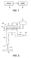
FIG. 1 is a schematic block diagram of an embodiment of a drop-on-demand drop emitting apparatus. -
FIG. 2 is a schematic block diagram of an embodiment of a drop generator that can be employed in the drop emitting apparatus ofFIG. 1 . -
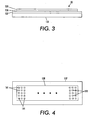
FIG. 3 is a schematic elevational view of an embodiment of an ink jet printhead assembly. -
FIG. 4 is a schematic plan view of an embodiment of a thin film interconnect circuit of the ink jet printhead assembly ofFIG. 3 . -
FIG. 5 is a schematic elevational sectional view of a portion of another embodiment of a thin film interconnect circuit of the ink jet printhead assembly. -
FIG. 6 is a schematic elevational sectional view of a portion of a further embodiment of a thin film interconnect circuit of the ink jet printhead assembly. -
FIG. 7 is a schematic elevational sectional view of a portion of another embodiment of a thin film interconnect circuit of the ink jet printhead assembly. -
FIG. 1 is a schematic block diagram of an embodiment of a drop-on-demand printing apparatus that includes acontroller 10 and aprinthead assembly 20 that can include a plurality of drop emitting drop generators. Thecontroller 10 selectively energizes the drop generators by providing a respective drive signal to each drop generator. Each of the drop generators can employ a piezoelectric transducer such as a ceramic piezoelectric transducer. As other examples, each of the drop generators can employ a shear-mode transducer, an annular constrictive transducer, an electrostrictive transducer, an electromagnetic transducer, or a magnetorestrictive transducer. Theprinthead assembly 20 can be formed of a stack of laminated sheets or plates, such as of stainless steel. -
FIG. 2 is a schematic block diagram of an embodiment of adrop generator 30 that can be employed in theprinthead assembly 20 of the printing apparatus shown inFIG. 1 . Thedrop generator 30 includes aninlet channel 31 that receivesink 33 from a manifold, reservoir or other ink containing structure. Theink 33 flows into a pressure orpump chamber 35 that is bounded on one side, for example, by aflexible diaphragm 37. A thin-film interconnect structure 38 is attached to the flexible diaphragm, for example so as to overlie thepressure chamber 35. Anelectromechanical transducer 39 is attached to the thinfilm interconnect structure 38. Theelectromechanical transducer 39 can be a piezoelectric transducer that includes apiezo element 41 disposed for example betweenelectrodes controller 10 via the thin-film interconnect structure 38, for example. Theelectrode 43 is connected to ground in common with thecontroller 10, while theelectrode 42 is actively driven to actuate theelectromechanical transducer 41 through theinterconnect structure 38. Actuation of theelectromechanical transducer 39 causes ink to flow from thepressure chamber 35 to a drop formingoutlet channel 45, from which anink drop 49 is emitted toward areceiver medium 48 that can be a transfer surface, for example. Theoutlet channel 45 can include a nozzle ororifice 47. - The
ink 33 can be melted or phase changed solid ink, and theelectromechanical transducer 39 can be a piezoelectric transducer that is operated in a bending mode, for example. -
FIG. 3 is a schematic elevational view of an embodiment of an inkjet printhead assembly 20 that can implement a plurality of drop generators 30 (FIG. 2 ), for example as an array of drop generators. The ink jet printhead assembly includes a fluid channel layer orsubstructure 131, adiaphragm layer 137 attached to thefluid channel layer 131, a thin-filminterconnect circuit layer 138 disposed on thediaphragm layer 137 and atransducer layer 139 attached to the thin-filminterconnect circuit layer 138. Thefluid channel layer 131 implements the fluid channels and chambers of thedrop generators 30, while thediaphragm layer 137 implements thediaphragms 37 of the drop generators. The thin-filminterconnect circuit layer 138 implements theinterconnect circuits 38, while thetransducer layer 139 implements theelectromechanical transducers 39 of thedrop generators 30. - By way of illustrative example, the
diaphragm layer 137 comprises a metal plate or sheet such as stainless steel that is attached or bonded to thefluid channel layer 131. Thediaphragm layer 137 can also comprise an electrically non-conductive material such as a ceramic. Also by way of illustrative example, thefluid channel layer 131 can comprise multiple laminated plates or sheets. Thetransducer layer 139 can comprise an array of kerfed ceramic transducers that are attached or bonded to the thin filminterconnect circuit layer 138, for example with an epoxy adhesive. -
FIG. 4 is a schematic plan view of an embodiment of a thin filminterconnect circuit layer 138 that includes raised contact pads orregions 191. The electromechanical transducers 39 (FIGS. 5-7 ) are conductively attached to respective raisedcontact pads 191, for example with conductive adhesive or a low temperature solder. As disclosed in various embodiments illustrated inFIGS. 5-7 , the raisedcontact regions 191 can be formed by a thin film structure that can include for example a mesa layer and a patterned conductive layer. The thinfilm interconnect circuit 138 can provide for electrical interconnection to the individualelectromechanical transducers 39. -
FIG. 5 is a schematic elevational sectional view of a portion of a further embodiment of a thin filminterconnect circuit layer 138 that can be used with an electrically conductive ornon-conductive diaphragm layer 137. The thin filminterconnect circuit layer 138 includes ablanket dielectric layer 213, a patternedconductive layer 215 disposed on theblanket dielectric layer 213, and aconductive mesa layer 211 comprising a plurality of conductive mesas overlying the patternedconductive layer 215. The conductive mesas and the underlying portions of theconductive layer 215 form raised contact regions orpads 191. Theinterconnect circuit layer 138 can further include a patterneddielectric layer 217 havingopenings 217A through which the raisedcontact pads 191 extend. The raisedcontact pads 191 are higher than the other layers of theinterconnect circuit layer 138, and comprise the highest portions of theinterconnect circuit layer 138. This facilitates the attachment of anelectromechanical transducer 39 to each of the raisedcontact pads 191. - In the embodiment schematically depicted in
FIG. 5 , the patternedmesa layer 211 can comprise a suitably patterned metal layer, and the patternedconductive layer 215 can also comprise a suitably patterned metal layer, for example. -
FIG. 6 is a schematic elevational sectional view of a portion of a further embodiment of a thin filminterconnect circuit layer 138 that can be used with an electrically conductive ornon-conductive diaphragm 137. Theinterconnect circuit layer 138 includes ablanket dielectric layer 213, amesa layer 211 comprising a plurality of mesas overlying theblanket dielectric layer 213, and a patternedconductive layer 215 overlying themesa layer 211. Themesa layer 211 can be electrically non-conductive (e.g., dielectric) or conductive (e.g., metal). The mesas and the overlying portions of the patternedconductive layer 215 form raised contact regions orpads 191. The thin filminterconnect circuit layer 138 can further include a patterneddielectric layer 217 havingopenings 217A through which the raisedcontact pads 191 extend. The raisedcontact pads 191 are higher than the other layers of theinterconnect circuit layer 138, and comprise the highest portions of theinterconnect layer 138. This facilitates the attachment of anelectromechanical transducer 39 to each of the raisedcontact pads 191. - In the embodiment schematically depicted in
FIG. 6 , themesa layer 211 can comprise a suitably patterned dielectric layer or metal layer, for example. The patternedconductive layer 215 can comprise a patterned metal layer. -
FIG. 7 is a schematic elevational sectional view of a portion of a further embodiment of a thin filminterconnect circuit layer 138 that can be used with an electricallynon-conductive diaphragm layer 137. The thin filminterconnect circuit layer 138 includes a patternedconductive layer 215 and aconductive mesa layer 211 comprising a plurality of mesas overlying the patternedconductive layer 215. The conductive mesas and the underlying portions of the patternedconductive layer 215 form raised contact regions orpads 191. The thin filminterconnect circuit layer 138 can further include a patterneddielectric layer 217 havingopenings 217A through which the raisedcontact pads 191 extend. The raisedcontact pads 191 are higher than the other layers of the thin filminterconnect circuit layer 138, and comprise the highest portions of theinterconnect layer 138. This facilitates the attachment of anelectromechanical transducer 39 to each of the raisedcontact pads 191. - In the embodiment schematically depicted in
FIG. 7 , the patternedconductive mesa layer 211 can comprise a suitably patterned metal layer, and the patternedconductive layer 215 can also comprise a suitably patterned metal layer, for example. - Each dielectric layer of the thin film
interconnect circuit layer 138 can comprise silicon oxide, silicon nitride, or silicon oxynitride, for example, and can have a thickness in the range of about 0.1 micrometers of about 5 micrometers. More specifically, each dielectric layer can have a thickness in the range of about 1 micrometers to about 2 micrometers. - Each conductive layer of the thin film
interconnect circuit layer 138 can comprise aluminum, chromium, nickel, tantalum or copper, for example, and can have a thickness in the range of about 0.1 micrometers of about 5 micrometers. More specifically, each conductive layer can have a thickness in the range of about 1 micrometers to about 2 micrometers.
Claims (10)
- A drop emitting apparatus comprising:a fluid channel layer (131),a diaphragm layer (137) disposed on the fluid channel layer;a blanket dielectric layer (213) disposed on the diaphragm layer;a thin film circuit (138) having raised contact regions (191) disposed on the blanket dielectric layer; anda plurality of electromechanical transducers (39) conductively attached to the raised contact regions.
- The drop emitting apparatus of claim 1 wherein the raised contact regions include dielectric mesas.
- The drop emitting apparatus of claim 1 wherein the raised contact regions include conductive mesas.
- The drop emitting apparatus of claim 1 wherein the thin film circuit comprises a mesa layer and a patterned conductive layer overlying the mesa layer.
- The drop emitting apparatus of claim 1 wherein the fluid channel layer receives melted solid ink.
- The drop emitting apparatus of claim 1 wherein the electromechanical transducers comprise piezoelectric transducers.
- The drop emitting apparatus of claim 1 wherein the fluid channel layer comprises a stack of patterned metal plates.
- A drop emitting apparatus comprising:a fluid channel layer,a dielectric diaphragm layer attached to the fluid channel layer;a patterned conductive layer disposed on the dielectric diaphragm layer;a plurality of conductive mesas disposed on the patterned conductive layer; anda plurality of piezoelectric transducers conductively attached to the conductive mesas.
- A drop emitting apparatus comprising:a fluid channel layer (131),a metal diaphragm layer (137) disposed on the fluid channel layer;a blanket dielectric layer (213) disposed on the diaphragm layera patterned conductive layer (215) disposed on the blanket dielectric layera plurality of conductive mesas (211) disposed on the patterned conductive layer; anda plurality of electromechanical transducers (39) conductively attached to the conductive mesas.
- A drop generator comprising:a pressure chamber (35);a diaphragm (137) forming a wall of the pressure chambera dielectric layer (213) disposed on the diaphragm;a thin film raised contact region (191) disposed on the dielectric layer,a piezoelectric transducer (39) conductively attached to the raised contact region;an outlet channel (45) connected to the pressure chamber; anda drop emitting nozzle (47) disposed at an end of the outlet channel.
Applications Claiming Priority (2)
| Application Number | Priority Date | Filing Date | Title |
|---|---|---|---|
| US10/702,935 US6955419B2 (en) | 2003-11-05 | 2003-11-05 | Ink jet apparatus |
| US702935 | 2003-11-05 |
Publications (2)
| Publication Number | Publication Date |
|---|---|
| EP1529641A1 EP1529641A1 (en) | 2005-05-11 |
| EP1529641B1 true EP1529641B1 (en) | 2008-06-18 |
Family
ID=34435557
Family Applications (1)
| Application Number | Title | Priority Date | Filing Date |
|---|---|---|---|
| EP04026225A Expired - Fee Related EP1529641B1 (en) | 2003-11-05 | 2004-11-04 | Ink jet apparatus |
Country Status (7)
| Country | Link |
|---|---|
| US (1) | US6955419B2 (en) |
| EP (1) | EP1529641B1 (en) |
| JP (1) | JP4634118B2 (en) |
| CN (1) | CN100430225C (en) |
| BR (1) | BRPI0404827A (en) |
| CA (1) | CA2487662C (en) |
| DE (1) | DE602004014458D1 (en) |
Families Citing this family (8)
| Publication number | Priority date | Publication date | Assignee | Title |
|---|---|---|---|---|
| US7048361B2 (en) * | 2003-11-05 | 2006-05-23 | Xerox Corporation | Ink jet apparatus |
| US7766463B2 (en) * | 2008-08-19 | 2010-08-03 | Xerox Corporation | Fluid dispensing subassembly with compliant film |
| US7934815B2 (en) * | 2008-08-19 | 2011-05-03 | Xerox Corporation | External fluid manifold with polymer compliant wall |
| BR112012030070B1 (en) * | 2010-05-27 | 2020-04-07 | Hewlett Packard Development Co | printhead, method for making an inkjet printhead and printing system |
| BR112013031746B1 (en) * | 2011-06-29 | 2020-10-20 | Hewlett-Packard Development Company, L.P | stack of piezoelectric inkjet inserts and piezoelectric printhead |
| US9144973B2 (en) * | 2012-04-29 | 2015-09-29 | Hewlett-Packard Development Company, L.P. | Piezoelectric inkjet die stack |
| US9662880B2 (en) | 2015-09-11 | 2017-05-30 | Xerox Corporation | Integrated thin film piezoelectric printhead |
| US10421266B2 (en) * | 2016-10-26 | 2019-09-24 | Xerox Corporation | Method of operating extruder heads in three-dimensional object printers |
Family Cites Families (9)
| Publication number | Priority date | Publication date | Assignee | Title |
|---|---|---|---|---|
| JPS5793160A (en) * | 1980-12-01 | 1982-06-10 | Hitachi Ltd | Ink drop injector |
| US4516140A (en) * | 1983-12-27 | 1985-05-07 | At&T Teletype Corporation | Print head actuator for an ink jet printer |
| JP3176245B2 (en) | 1995-03-23 | 2001-06-11 | シャープ株式会社 | Inkjet head |
| US5658471A (en) * | 1995-09-22 | 1997-08-19 | Lexmark International, Inc. | Fabrication of thermal ink-jet feed slots in a silicon substrate |
| US5755909A (en) * | 1996-06-26 | 1998-05-26 | Spectra, Inc. | Electroding of ceramic piezoelectric transducers |
| JP3019845B1 (en) * | 1997-11-25 | 2000-03-13 | セイコーエプソン株式会社 | Ink jet recording head and ink jet recording apparatus |
| JP3517876B2 (en) * | 1998-10-14 | 2004-04-12 | セイコーエプソン株式会社 | Ferroelectric thin film element manufacturing method, ink jet recording head, and ink jet printer |
| JP4221929B2 (en) * | 2000-03-31 | 2009-02-12 | 富士フイルム株式会社 | Multi-nozzle ink jet head |
| US6457814B1 (en) * | 2000-12-20 | 2002-10-01 | Hewlett-Packard Company | Fluid-jet printhead and method of fabricating a fluid-jet printhead |
-
2003
- 2003-11-05 US US10/702,935 patent/US6955419B2/en not_active Expired - Lifetime
-
2004
- 2004-11-01 CA CA002487662A patent/CA2487662C/en not_active Expired - Fee Related
- 2004-11-02 JP JP2004319012A patent/JP4634118B2/en not_active Expired - Fee Related
- 2004-11-04 EP EP04026225A patent/EP1529641B1/en not_active Expired - Fee Related
- 2004-11-04 DE DE602004014458T patent/DE602004014458D1/en active Active
- 2004-11-05 BR BR0404827-0A patent/BRPI0404827A/en not_active IP Right Cessation
- 2004-11-05 CN CNB200410092241XA patent/CN100430225C/en not_active Expired - Fee Related
Also Published As
| Publication number | Publication date |
|---|---|
| CA2487662A1 (en) | 2005-05-05 |
| CN100430225C (en) | 2008-11-05 |
| US6955419B2 (en) | 2005-10-18 |
| EP1529641A1 (en) | 2005-05-11 |
| CN1613647A (en) | 2005-05-11 |
| JP2005138588A (en) | 2005-06-02 |
| DE602004014458D1 (en) | 2008-07-31 |
| JP4634118B2 (en) | 2011-02-16 |
| US20050093930A1 (en) | 2005-05-05 |
| BRPI0404827A (en) | 2005-06-28 |
| CA2487662C (en) | 2006-08-22 |
Similar Documents
| Publication | Publication Date | Title |
|---|---|---|
| EP2253473B1 (en) | Piezoelectric ink jet module | |
| US8397359B2 (en) | Method of manufacturing a drop generator | |
| JP2015147374A (en) | Liquid ejection head and recording apparatus | |
| EP1795355A1 (en) | Drop generator | |
| US7651200B2 (en) | Ink jet head | |
| EP1529641B1 (en) | Ink jet apparatus | |
| EP1529642B1 (en) | Ink jet apparatus | |
| JP4563786B2 (en) | Liquid ejecting apparatus and driving method thereof | |
| JP5893977B2 (en) | Liquid discharge head and recording apparatus using the same | |
| JP4602640B2 (en) | Inkjet print head | |
| US20050045272A1 (en) | Laser removal of adhesive | |
| EP1431035A1 (en) | Ink jet apparatus | |
| US7143488B2 (en) | Drop emitting apparatus | |
| US7665828B2 (en) | Drop generator | |
| JP2011131462A (en) | Liquid discharge head and recording apparatus using the same | |
| JP4392200B2 (en) | Print head and electronics | |
| JP2005007868A (en) | Piezo-electric ink jet head | |
| JP2009051188A (en) | Liquid discharge device | |
| JP2010076265A (en) | Liquid discharge head and printer using it | |
| JP2013244722A (en) | Liquid ejection head and recorder using the same |
Legal Events
| Date | Code | Title | Description |
|---|---|---|---|
| PUAI | Public reference made under article 153(3) epc to a published international application that has entered the european phase |
Free format text: ORIGINAL CODE: 0009012 |
|
| AK | Designated contracting states |
Kind code of ref document: A1 Designated state(s): AT BE BG CH CY CZ DE DK EE ES FI FR GB GR HU IE IS IT LI LU MC NL PL PT RO SE SI SK TR |
|
| AX | Request for extension of the european patent |
Extension state: AL HR LT LV MK YU |
|
| 17P | Request for examination filed |
Effective date: 20051111 |
|
| AKX | Designation fees paid |
Designated state(s): DE FR GB |
|
| GRAP | Despatch of communication of intention to grant a patent |
Free format text: ORIGINAL CODE: EPIDOSNIGR1 |
|
| GRAS | Grant fee paid |
Free format text: ORIGINAL CODE: EPIDOSNIGR3 |
|
| GRAA | (expected) grant |
Free format text: ORIGINAL CODE: 0009210 |
|
| AK | Designated contracting states |
Kind code of ref document: B1 Designated state(s): DE FR GB |
|
| REG | Reference to a national code |
Ref country code: GB Ref legal event code: FG4D |
|
| REF | Corresponds to: |
Ref document number: 602004014458 Country of ref document: DE Date of ref document: 20080731 Kind code of ref document: P |
|
| PLBE | No opposition filed within time limit |
Free format text: ORIGINAL CODE: 0009261 |
|
| STAA | Information on the status of an ep patent application or granted ep patent |
Free format text: STATUS: NO OPPOSITION FILED WITHIN TIME LIMIT |
|
| 26N | No opposition filed |
Effective date: 20090319 |
|
| REG | Reference to a national code |
Ref country code: FR Ref legal event code: PLFP Year of fee payment: 12 |
|
| REG | Reference to a national code |
Ref country code: FR Ref legal event code: PLFP Year of fee payment: 13 |
|
| PGFP | Annual fee paid to national office [announced via postgrant information from national office to epo] |
Ref country code: DE Payment date: 20161020 Year of fee payment: 13 Ref country code: GB Payment date: 20161027 Year of fee payment: 13 Ref country code: FR Payment date: 20161024 Year of fee payment: 13 |
|
| REG | Reference to a national code |
Ref country code: DE Ref legal event code: R119 Ref document number: 602004014458 Country of ref document: DE |
|
| GBPC | Gb: european patent ceased through non-payment of renewal fee |
Effective date: 20171104 |
|
| REG | Reference to a national code |
Ref country code: FR Ref legal event code: ST Effective date: 20180731 |
|
| PG25 | Lapsed in a contracting state [announced via postgrant information from national office to epo] |
Ref country code: FR Free format text: LAPSE BECAUSE OF NON-PAYMENT OF DUE FEES Effective date: 20171130 Ref country code: DE Free format text: LAPSE BECAUSE OF NON-PAYMENT OF DUE FEES Effective date: 20180602 |
|
| PG25 | Lapsed in a contracting state [announced via postgrant information from national office to epo] |
Ref country code: GB Free format text: LAPSE BECAUSE OF NON-PAYMENT OF DUE FEES Effective date: 20171104 |