EP1528677A1 - Transformateur à couplage acoustique de couches minces avec deux éléments piézoélectriques à axe-c inversé - Google Patents
Transformateur à couplage acoustique de couches minces avec deux éléments piézoélectriques à axe-c inversé Download PDFInfo
- Publication number
- EP1528677A1 EP1528677A1 EP04015552A EP04015552A EP1528677A1 EP 1528677 A1 EP1528677 A1 EP 1528677A1 EP 04015552 A EP04015552 A EP 04015552A EP 04015552 A EP04015552 A EP 04015552A EP 1528677 A1 EP1528677 A1 EP 1528677A1
- Authority
- EP
- European Patent Office
- Prior art keywords
- layer
- fbar
- electrodes
- fbars
- piezoelectric
- Prior art date
- Legal status (The legal status is an assumption and is not a legal conclusion. Google has not performed a legal analysis and makes no representation as to the accuracy of the status listed.)
- Granted
Links
- 239000000463 material Substances 0.000 claims description 264
- 229910052751 metal Inorganic materials 0.000 claims description 60
- 239000002184 metal Substances 0.000 claims description 60
- 238000000151 deposition Methods 0.000 claims description 39
- 238000000034 method Methods 0.000 claims description 35
- 238000004519 manufacturing process Methods 0.000 claims description 21
- 238000000059 patterning Methods 0.000 claims description 19
- 230000008021 deposition Effects 0.000 claims description 18
- 239000004642 Polyimide Substances 0.000 claims description 12
- 229920001721 polyimide Polymers 0.000 claims description 12
- 230000015572 biosynthetic process Effects 0.000 claims description 10
- 229920000052 poly(p-xylylene) Polymers 0.000 claims description 8
- 239000004033 plastic Substances 0.000 claims description 7
- -1 poly(para-xylylene) Polymers 0.000 claims description 4
- 239000010410 layer Substances 0.000 description 220
- 239000010409 thin film Substances 0.000 description 39
- ZOKXTWBITQBERF-UHFFFAOYSA-N Molybdenum Chemical compound [Mo] ZOKXTWBITQBERF-UHFFFAOYSA-N 0.000 description 22
- 229910052750 molybdenum Inorganic materials 0.000 description 22
- 239000011733 molybdenum Substances 0.000 description 22
- 230000008569 process Effects 0.000 description 22
- 238000004544 sputter deposition Methods 0.000 description 18
- 238000001312 dry etching Methods 0.000 description 15
- 239000003870 refractory metal Substances 0.000 description 15
- VYPSYNLAJGMNEJ-UHFFFAOYSA-N Silicium dioxide Chemical compound O=[Si]=O VYPSYNLAJGMNEJ-UHFFFAOYSA-N 0.000 description 14
- KWYUFKZDYYNOTN-UHFFFAOYSA-M Potassium hydroxide Chemical compound [OH-].[K+] KWYUFKZDYYNOTN-UHFFFAOYSA-M 0.000 description 12
- BASFCYQUMIYNBI-UHFFFAOYSA-N platinum Chemical group [Pt] BASFCYQUMIYNBI-UHFFFAOYSA-N 0.000 description 12
- 238000002955 isolation Methods 0.000 description 11
- 230000008878 coupling Effects 0.000 description 10
- 238000010168 coupling process Methods 0.000 description 10
- 238000005859 coupling reaction Methods 0.000 description 10
- 238000005137 deposition process Methods 0.000 description 10
- 239000011241 protective layer Substances 0.000 description 10
- 230000008859 change Effects 0.000 description 9
- 239000010408 film Substances 0.000 description 8
- 239000000758 substrate Substances 0.000 description 8
- 239000000377 silicon dioxide Substances 0.000 description 7
- 238000004804 winding Methods 0.000 description 7
- ZAMOUSCENKQFHK-UHFFFAOYSA-N Chlorine atom Chemical compound [Cl] ZAMOUSCENKQFHK-UHFFFAOYSA-N 0.000 description 6
- 230000001413 cellular effect Effects 0.000 description 6
- 239000000460 chlorine Substances 0.000 description 6
- 229910052801 chlorine Inorganic materials 0.000 description 6
- HFGPZNIAWCZYJU-UHFFFAOYSA-N lead zirconate titanate Chemical compound [O-2].[O-2].[O-2].[O-2].[O-2].[Ti+4].[Zr+4].[Pb+2] HFGPZNIAWCZYJU-UHFFFAOYSA-N 0.000 description 6
- 229910052697 platinum Inorganic materials 0.000 description 6
- 230000009466 transformation Effects 0.000 description 6
- 238000001039 wet etching Methods 0.000 description 6
- PMHQVHHXPFUNSP-UHFFFAOYSA-M copper(1+);methylsulfanylmethane;bromide Chemical compound Br[Cu].CSC PMHQVHHXPFUNSP-UHFFFAOYSA-M 0.000 description 5
- 230000005684 electric field Effects 0.000 description 5
- 229910052741 iridium Inorganic materials 0.000 description 5
- GKOZUEZYRPOHIO-UHFFFAOYSA-N iridium atom Chemical compound [Ir] GKOZUEZYRPOHIO-UHFFFAOYSA-N 0.000 description 5
- 229920002120 photoresistant polymer Polymers 0.000 description 5
- 230000004044 response Effects 0.000 description 5
- XLOMVQKBTHCTTD-UHFFFAOYSA-N Zinc monoxide Chemical compound [Zn]=O XLOMVQKBTHCTTD-UHFFFAOYSA-N 0.000 description 4
- JRPBQTZRNDNNOP-UHFFFAOYSA-N barium titanate Chemical compound [Ba+2].[Ba+2].[O-][Ti]([O-])([O-])[O-] JRPBQTZRNDNNOP-UHFFFAOYSA-N 0.000 description 4
- 229910002113 barium titanate Inorganic materials 0.000 description 4
- 238000003780 insertion Methods 0.000 description 4
- 230000037431 insertion Effects 0.000 description 4
- 239000005360 phosphosilicate glass Substances 0.000 description 4
- 238000004528 spin coating Methods 0.000 description 4
- QVGXLLKOCUKJST-UHFFFAOYSA-N atomic oxygen Chemical compound [O] QVGXLLKOCUKJST-UHFFFAOYSA-N 0.000 description 3
- 230000015556 catabolic process Effects 0.000 description 3
- 239000000470 constituent Substances 0.000 description 3
- 238000006731 degradation reaction Methods 0.000 description 3
- 238000005530 etching Methods 0.000 description 3
- 230000004907 flux Effects 0.000 description 3
- 239000001301 oxygen Substances 0.000 description 3
- 229910052760 oxygen Inorganic materials 0.000 description 3
- WUPHOULIZUERAE-UHFFFAOYSA-N 3-(oxolan-2-yl)propanoic acid Chemical compound OC(=O)CCC1CCCO1 WUPHOULIZUERAE-UHFFFAOYSA-N 0.000 description 2
- PIGFYZPCRLYGLF-UHFFFAOYSA-N Aluminum nitride Chemical compound [Al]#N PIGFYZPCRLYGLF-UHFFFAOYSA-N 0.000 description 2
- IJGRMHOSHXDMSA-UHFFFAOYSA-N Atomic nitrogen Chemical compound N#N IJGRMHOSHXDMSA-UHFFFAOYSA-N 0.000 description 2
- KRHYYFGTRYWZRS-UHFFFAOYSA-N Fluorane Chemical compound F KRHYYFGTRYWZRS-UHFFFAOYSA-N 0.000 description 2
- GWEVSGVZZGPLCZ-UHFFFAOYSA-N Titan oxide Chemical compound O=[Ti]=O GWEVSGVZZGPLCZ-UHFFFAOYSA-N 0.000 description 2
- 229910052980 cadmium sulfide Inorganic materials 0.000 description 2
- 238000005229 chemical vapour deposition Methods 0.000 description 2
- 230000001788 irregular Effects 0.000 description 2
- 238000004518 low pressure chemical vapour deposition Methods 0.000 description 2
- 238000001552 radio frequency sputter deposition Methods 0.000 description 2
- 239000010979 ruby Substances 0.000 description 2
- 229910001750 ruby Inorganic materials 0.000 description 2
- 230000001131 transforming effect Effects 0.000 description 2
- 238000001771 vacuum deposition Methods 0.000 description 2
- 239000011787 zinc oxide Substances 0.000 description 2
- RTAQQCXQSZGOHL-UHFFFAOYSA-N Titanium Chemical compound [Ti] RTAQQCXQSZGOHL-UHFFFAOYSA-N 0.000 description 1
- 238000010923 batch production Methods 0.000 description 1
- 230000005540 biological transmission Effects 0.000 description 1
- 239000013078 crystal Substances 0.000 description 1
- 230000001419 dependent effect Effects 0.000 description 1
- 239000000539 dimer Substances 0.000 description 1
- 238000007598 dipping method Methods 0.000 description 1
- 230000000694 effects Effects 0.000 description 1
- 238000010292 electrical insulation Methods 0.000 description 1
- 239000007772 electrode material Substances 0.000 description 1
- 238000001704 evaporation Methods 0.000 description 1
- 230000008020 evaporation Effects 0.000 description 1
- PCHJSUWPFVWCPO-UHFFFAOYSA-N gold Chemical compound [Au] PCHJSUWPFVWCPO-UHFFFAOYSA-N 0.000 description 1
- 229910052737 gold Inorganic materials 0.000 description 1
- 239000010931 gold Substances 0.000 description 1
- FMEVCTOFYHBTTB-UHFFFAOYSA-N iridium molybdenum Chemical compound [Mo].[Ir].[Ir].[Ir] FMEVCTOFYHBTTB-UHFFFAOYSA-N 0.000 description 1
- ORUIBWPALBXDOA-UHFFFAOYSA-L magnesium fluoride Chemical compound [F-].[F-].[Mg+2] ORUIBWPALBXDOA-UHFFFAOYSA-L 0.000 description 1
- 229910001635 magnesium fluoride Inorganic materials 0.000 description 1
- 229910021421 monocrystalline silicon Inorganic materials 0.000 description 1
- 229910052758 niobium Inorganic materials 0.000 description 1
- 239000010955 niobium Substances 0.000 description 1
- GUCVJGMIXFAOAE-UHFFFAOYSA-N niobium atom Chemical compound [Nb] GUCVJGMIXFAOAE-UHFFFAOYSA-N 0.000 description 1
- 229910052757 nitrogen Inorganic materials 0.000 description 1
- 239000013307 optical fiber Substances 0.000 description 1
- 239000002245 particle Substances 0.000 description 1
- 230000035699 permeability Effects 0.000 description 1
- 238000000206 photolithography Methods 0.000 description 1
- 229920003223 poly(pyromellitimide-1,4-diphenyl ether) Polymers 0.000 description 1
- 239000002243 precursor Substances 0.000 description 1
- 230000001681 protective effect Effects 0.000 description 1
- 238000000926 separation method Methods 0.000 description 1
- 235000012239 silicon dioxide Nutrition 0.000 description 1
- 238000005507 spraying Methods 0.000 description 1
- 239000000725 suspension Substances 0.000 description 1
- 229910052719 titanium Inorganic materials 0.000 description 1
- 239000010936 titanium Substances 0.000 description 1
- 239000004408 titanium dioxide Substances 0.000 description 1
- WFKWXMTUELFFGS-UHFFFAOYSA-N tungsten Chemical compound [W] WFKWXMTUELFFGS-UHFFFAOYSA-N 0.000 description 1
- 229910052721 tungsten Inorganic materials 0.000 description 1
- 239000010937 tungsten Substances 0.000 description 1
Images


Classifications
-
- H—ELECTRICITY
- H03—ELECTRONIC CIRCUITRY
- H03H—IMPEDANCE NETWORKS, e.g. RESONANT CIRCUITS; RESONATORS
- H03H9/00—Networks comprising electromechanical or electro-acoustic devices; Electromechanical resonators
- H03H9/46—Filters
- H03H9/54—Filters comprising resonators of piezo-electric or electrostrictive material
- H03H9/58—Multiple crystal filters
- H03H9/60—Electric coupling means therefor
- H03H9/605—Electric coupling means therefor consisting of a ladder configuration
-
- H—ELECTRICITY
- H03—ELECTRONIC CIRCUITRY
- H03H—IMPEDANCE NETWORKS, e.g. RESONANT CIRCUITS; RESONATORS
- H03H9/00—Networks comprising electromechanical or electro-acoustic devices; Electromechanical resonators
- H03H9/02—Details
- H03H9/125—Driving means, e.g. electrodes, coils
- H03H9/13—Driving means, e.g. electrodes, coils for networks consisting of piezoelectric or electrostrictive materials
- H03H9/132—Driving means, e.g. electrodes, coils for networks consisting of piezoelectric or electrostrictive materials characterized by a particular shape
-
- H—ELECTRICITY
- H03—ELECTRONIC CIRCUITRY
- H03H—IMPEDANCE NETWORKS, e.g. RESONANT CIRCUITS; RESONATORS
- H03H9/00—Networks comprising electromechanical or electro-acoustic devices; Electromechanical resonators
- H03H9/46—Filters
- H03H9/54—Filters comprising resonators of piezo-electric or electrostrictive material
- H03H9/58—Multiple crystal filters
- H03H9/582—Multiple crystal filters implemented with thin-film techniques
- H03H9/583—Multiple crystal filters implemented with thin-film techniques comprising a plurality of piezoelectric layers acoustically coupled
- H03H9/584—Coupled Resonator Filters [CFR]
-
- H—ELECTRICITY
- H03—ELECTRONIC CIRCUITRY
- H03H—IMPEDANCE NETWORKS, e.g. RESONANT CIRCUITS; RESONATORS
- H03H9/00—Networks comprising electromechanical or electro-acoustic devices; Electromechanical resonators
- H03H9/46—Filters
- H03H9/54—Filters comprising resonators of piezo-electric or electrostrictive material
- H03H9/58—Multiple crystal filters
- H03H9/582—Multiple crystal filters implemented with thin-film techniques
- H03H9/586—Means for mounting to a substrate, i.e. means constituting the material interface confining the waves to a volume
- H03H9/587—Air-gaps
-
- Y—GENERAL TAGGING OF NEW TECHNOLOGICAL DEVELOPMENTS; GENERAL TAGGING OF CROSS-SECTIONAL TECHNOLOGIES SPANNING OVER SEVERAL SECTIONS OF THE IPC; TECHNICAL SUBJECTS COVERED BY FORMER USPC CROSS-REFERENCE ART COLLECTIONS [XRACs] AND DIGESTS
- Y10—TECHNICAL SUBJECTS COVERED BY FORMER USPC
- Y10T—TECHNICAL SUBJECTS COVERED BY FORMER US CLASSIFICATION
- Y10T29/00—Metal working
- Y10T29/42—Piezoelectric device making
-
- Y—GENERAL TAGGING OF NEW TECHNOLOGICAL DEVELOPMENTS; GENERAL TAGGING OF CROSS-SECTIONAL TECHNOLOGIES SPANNING OVER SEVERAL SECTIONS OF THE IPC; TECHNICAL SUBJECTS COVERED BY FORMER USPC CROSS-REFERENCE ART COLLECTIONS [XRACs] AND DIGESTS
- Y10—TECHNICAL SUBJECTS COVERED BY FORMER USPC
- Y10T—TECHNICAL SUBJECTS COVERED BY FORMER US CLASSIFICATION
- Y10T29/00—Metal working
- Y10T29/49—Method of mechanical manufacture
- Y10T29/49002—Electrical device making
- Y10T29/4902—Electromagnet, transformer or inductor
-
- Y—GENERAL TAGGING OF NEW TECHNOLOGICAL DEVELOPMENTS; GENERAL TAGGING OF CROSS-SECTIONAL TECHNOLOGIES SPANNING OVER SEVERAL SECTIONS OF THE IPC; TECHNICAL SUBJECTS COVERED BY FORMER USPC CROSS-REFERENCE ART COLLECTIONS [XRACs] AND DIGESTS
- Y10—TECHNICAL SUBJECTS COVERED BY FORMER USPC
- Y10T—TECHNICAL SUBJECTS COVERED BY FORMER US CLASSIFICATION
- Y10T29/00—Metal working
- Y10T29/49—Method of mechanical manufacture
- Y10T29/49002—Electrical device making
- Y10T29/49117—Conductor or circuit manufacturing
- Y10T29/49124—On flat or curved insulated base, e.g., printed circuit, etc.
- Y10T29/49128—Assembling formed circuit to base
-
- Y—GENERAL TAGGING OF NEW TECHNOLOGICAL DEVELOPMENTS; GENERAL TAGGING OF CROSS-SECTIONAL TECHNOLOGIES SPANNING OVER SEVERAL SECTIONS OF THE IPC; TECHNICAL SUBJECTS COVERED BY FORMER USPC CROSS-REFERENCE ART COLLECTIONS [XRACs] AND DIGESTS
- Y10—TECHNICAL SUBJECTS COVERED BY FORMER USPC
- Y10T—TECHNICAL SUBJECTS COVERED BY FORMER US CLASSIFICATION
- Y10T29/00—Metal working
- Y10T29/49—Method of mechanical manufacture
- Y10T29/49002—Electrical device making
- Y10T29/49117—Conductor or circuit manufacturing
- Y10T29/49124—On flat or curved insulated base, e.g., printed circuit, etc.
- Y10T29/49155—Manufacturing circuit on or in base
Definitions
- Transformers are used in many types of electronic device to perform such functions as transforming impedances, linking single-ended circuitry with balanced circuitry or vice versa and providing electrical isolation. However, not all transformers have all of these properties. For example, an auto-transformer does not provide electrical isolation.
- Transformers operating at audio and radio frequencies up to VHF are commonly built as coupled primary and secondary windings around a high permeability core. Current in the windings generates a magnetic flux. The core contains the magnetic flux and increases the coupling between the windings.
- a transformer operable in this frequency range can also be realized using an optical-coupler.
- An opto-coupler used in this mode is referred to in the art as an opto-isolator.
- the input electrical signal is converted to a different form (i.e., a magnetic flux or photons) that interacts with an appropriate transforming structure (i.e., another winding or a light detector), and is re-constituted as an electrical signal at the output.
- an opto-coupler converts an input electrical signal to photons using a light-emitting diode.
- the photons pass through an optical fiber or free space that provides isolation.
- a photodiode illuminated by the photons generates an output electrical signal from the photon stream.
- the output electrical signal is a replica of the input electrical signal
- transformers At UHF and microwave frequencies, coil-based transformers become impractical due to such factors as losses in the core, losses in the windings, capacitance between the windings, and a difficulty to make them small enough to prevent wavelength-related problems.
- Transformers for such frequencies are based on quarter-wavelength transmission lines, e.g., Marchand type, series input/parallel output connected lines, etc.
- Transformers also exist that are based on micro-machined coupled coils sets and are small enough that wavelength effects are unimportant. However such transformers have issues with high insertion loss.
- transformers just described for use at UHF and microwave frequencies have dimensions that make them less desirable for use in modem miniature, high-density applications such as cellular telephones.
- Such transformers also tend to be high in cost because they are not capable of being manufactured by a batch process and because they are essentially an off-chip solution.
- transformers typically have a bandwidth that is acceptable for use in cellular telephones, they typically have an insertion loss greater than 1 dB, which is too high.
- Opto-couplers are not used at UHF and microwave frequencies due to the junction capacitance of the input LED, non-linearities inherent in the photodetector limited power handling capability and insufficient isolation to give good common mode rejection.
- a transformer capable of providing one or more of the following attributes at electrical frequencies in the range from UHF to microwave: impedance transformation, coupling between balanced and unbalanced circuits and electrical isolation.
- impedance transformation a transformer that has a low insertion loss, a bandwidth sufficient to accommodate the frequency range of cellular telephone RF signals, for example, a size smaller than transformers currently used in cellular telephones and a low manufacturing cost.
- the invention provides an acoustically-coupled transformer having a first stacked bulk acoustic resonator (SBAR) and a second SBAR.
- SBAR first stacked bulk acoustic resonator
- Each of the SBARs has a lower film bulk acoustic resonator (FBAR) and an upper FBAR, and an acoustic decoupler between the FBARs.
- the upper FBAR is stacked atop the lower FBAR.
- Each FBAR has opposed planar electrodes and a piezoelectric element between the electrodes.
- the piezoelectric element is characterized by a c-axis.
- the c-axes of the piezoelectric elements of the lower FBARs are opposite in direction, and the c-axes of the piezoelectric elements of the upper FBARs are opposite in direction.
- the transformer additionally has a first electrical circuit connecting the lower FBAR of the first SBAR to the lower FBAR of the second SBAR, and a second electrical circuit connecting the upper FBAR of the first SBAR to the upper FBARs of the second SBAR.
- the invention provides a method of making an acoustically-coupled transformer.
- a first stacked bulk acoustic resonator (SBAR) and a second SBAR are fabricated.
- the SBARs are fabricated by forming lower film bulk acoustic resonators (FBARs) and upper FBARs and locating an acoustic decoupler between the lower FBAR and the upper FBAR of each SBAR.
- FBARs lower film bulk acoustic resonators
- Each of the FBARs has opposed planar electrodes and a piezoelectric element between the electrodes.
- the piezoelectric element is characterized by a c-axis.
- the c-axes of the piezoelectric elements of the lower FBARs are set opposite in direction, and the c-axes of the upper FBARs are set opposite in direction. Additionally in the method, the lower FBAR of the first SBAR to the lower FBAR of the second SBAR are electrically connected and the upper FBAR of the first SBAR to the upper FBAR of the second SBAR are electrically connected.
- a metal layer is deposited and is patterned to define a pair of the electrodes, and a layer of piezoelectric material is deposited on the electrodes.
- the c-axes of the piezoelectric elements are set opposite in direction by depositing a seed layer of reverse c-axis piezoelectric material on one of the electrodes prior to depositing the layer of piezoelectric material.
- a metal layer is deposited and is patterned to define a pair of the electrodes, and a layer of piezoelectric material is deposited on the electrodes.
- the deposited layer has a region of reverse c-axis material on one of the electrodes and a region of normal c-axis material on the other of the electrodes.
- the c-axes of the piezoelectric elements are set opposite in direction by depositing the regions using different deposition conditions.
- a metal layer is deposited and is patterned to define a pair of first electrodes, a layer of ferroelectric piezoelectric material is deposited over the first electrodes, and an additional metal layer is deposited and is patterned to define pair of second electrodes opposite the first electrodes.
- the c-axes of the piezoelectric elements are set opposite in direction by applying a poling voltage of a nominal polarity between one of the first electrodes and an opposed one of the second electrodes, and a poling voltage of an opposite polarity between the other of the first electrodes and the other of the second electrodes.
- Embodiments of an acoustically-coupled transformer in accordance with the invention are capable of providing one or more of the following attributes at electrical frequencies in the range from UHF to microwave: impedance transformation, coupling between balanced and unbalanced circuits and electrical isolation.
- Such embodiments typically have a low insertion loss, a bandwidth sufficient to accommodate the frequency range of cellular telephone RF signals, for example, a size smaller than transformers currently used in cellular telephones and a low manufacturing cost.
- FBARs Film bulk acoustic resonators
- Ruby et al. in United States patent no. 5,587,620 entitled Tunable Thin Film Acoustic Resonators and Method of Making Same, now assigned to the assignee of this disclosure and incorporated in this disclosure by reference.
- Ruby's disclosure also discloses a stacked film bulk acoustic resonator (SBAR) composed of two layers of piezoelectric material interleaved with three planar electrodes.
- SBAR stacked film bulk acoustic resonator
- Ruby's SBAR can be regarded as being composed of a stacked pair of FBARs in which one electrode is common to both FBARs, and will be referred to as a common-electrode SBAR.
- the common electrode renders the common-electrode SBAR incapable of linking balanced to unbalanced circuits and vice versa and of providing electrical isolation between primary and secondary. Moreover, the common electrode SBAR exhibits an extremely narrow pass bandwidth that makes it unsuitable for use in most applications. The narrow pass bandwidth is the result of the common electrode, which over couples acoustic energy between the FBARs.
- United States patent application serial no. 10/699,481 discloses a thin-film acoustically-coupled transformer composed of a pair of interconnected SBARs in which each of the SBARs incorporates an acoustic decoupler interposed between its constituent FBARs.
- the acoustic decoupler provides electrical isolation between primary and secondary and eliminates the overcoupling of acoustic energy between the FBARs which gives the thin-film acoustically-coupled transformer a useable bandwidth.
- a film bulk acoustic resonator is a polarity-dependent device as a result of polarity dependence of the piezoelectric material that constitutes part of the FBAR.
- a voltage of a given polarity applied between the electrodes of the FBAR will cause the thickness of the FBAR to change in a first direction, whereas the same voltage of the opposite polarity will cause the thickness of the FBAR to change in a second direction, opposite the first direction.
- a voltage of the given polarity will cause the thickness of the FBAR to increase whereas a voltage of the opposite polarity will cause the FBAR to decrease.
- the thickness of the FBAR is the dimension of the FBAR between the electrodes.
- a mechanical stress applied to the FBAR that causes the thickness of the FBAR to change in a first direction will generate a voltage of the given polarity between the electrodes of the FBAR
- a mechanical stress that causes the thickness of the FBAR to change in a second direction, opposite the first direction will generate a voltage of the opposite polarity between the electrodes of the FBAR.
- a mechanical stress applied to the FBAR that causes the thickness of the FBAR to increase will generate a voltage of the given polarity
- a mechanical stress that causes the thickness of the FBAR to decrease will generate a voltage of the opposite polarity.
- Piezoelectric materials such as aluminum nitride (AlN) in the crystal class 6mm have a hexagonal unit cell with an a-axis and a b-axis in the hexagonal plane and a c-axis orthogonal to the hexagonal plane.
- the direction of the c-axis of the piezoelectric material of the FBAR determines the relationship between the polarity of the voltage and the direction of change in the thickness of the FBAR.
- the above examples are obtained using an FBAR in which the piezoelectric material has its c-axis oriented in a given direction.
- a voltage of the given polarity applied between the electrodes of the FBAR will cause the thickness of the FBAR to change in the second direction, whereas a voltage of the opposite polarity will cause the thickness of the FBAR to change in a first direction.
- a mechanical stress applied to the FBAR that causes the thickness of the FBAR to change in a first direction will generate a voltage of the opposite polarity between the electrodes of the FBAR whereas a mechanical stress that causes the thickness of the FBAR to change in a second direction, opposite the first direction, will generate a voltage of the given polarity between the electrodes of the FBAR.
- Piezoelectric material whose c-axis extends towards the substrate over which the FBAR is suspended will be referred to herein as reverse c-axis material .
- Piezoelectric material whose c-axis extends away from the substrate over which the FBARs are suspended will be referred to herein as normal c-axis material .
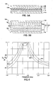
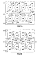
- FIGS 1A-1C show a plan view and two cross-sectional views, respectively, of an exemplary embodiment 100 of a thin-film acoustically-coupled transformer in accordance with the invention.
- Acoustically-coupled transformer 100 is capable of linking single-ended circuitry with balanced circuitry or vice versa, provides electrical isolation between primary and secondary and is electrically balanced.
- Acoustically-coupled transformer 100 is a low-impedance transformer having an impedance transformation ratio of 1:1.
- Acoustically-coupled transformer 100 is composed of two stacked bulk acoustic resonators (SBARs) 106 and 108. Each SBAR is composed of a lower film bulk acoustic resonator (FBAR) and an upper FBAR and an acoustic decoupler between the FBARs. The upper FBAR is stacked atop the lower FBAR. Transformer 100 is additionally composed of an electrical circuit that connects the lower FBAR of SBAR 106 to the lower FBAR of SBAR 108, and an electrical circuit that connects the upper FBAR of SBAR 106 to the upper FBAR of SBAR 108. SBARs incorporating acoustic decouplers are described in more detail in United States patent application serial no. 10/699,289 assigned to the assignee of this disclosure and incorporated herein in its entirety by reference.
- SBAR 106 is composed of a lower FBAR 110 and an upper FBAR 120 and an acoustic decoupler 130 between FBARs 110 and 120.
- Upper FBAR 120 is stacked atop lower FBAR 110.
- Acoustic decoupler 130 controls the coupling of acoustic energy between FBARs 110 and 120.
- SBAR 108 is composed of a lower FBAR 150 and an upper FBAR 160 and an acoustic decoupler 170 between FBARs 150 and 160.
- Upper FBAR 160 is stacked atop lower FBAR 150.
- Acoustic decoupler 170 controls the coupling of acoustic energy between FBARs 150 and 160.
- Lower FBAR 110 is composed of opposed planar electrodes 112 and 114 and a piezoelectric element 116 between the electrodes.
- Upper FBAR 120 is composed of opposed planar electrodes 122 and 124 and a piezoelectric element 126 between the electrodes.
- Lower FBAR 150 is composed of opposed planar electrodes 152 and 154 and a piezoelectric element 156 between the electrodes.
- Upper FBAR 160 is composed of opposed planar electrodes 162 and 164 and a piezoelectric element 166 between the electrodes.
- SBAR 106 and SBAR 108 are suspended over a cavity 104 defined in a substrate 102. Suspending the SBARs over a cavity allows the FBARs of the SBARs to resonate mechanically. Other suspension schemes that allow the FBARs to resonate mechanically are possible.
- the SBARs can be located over a mismatched acoustic Bragg reflector (not shown) formed in or on substrate 102, as disclosed by Lakin in United States patent no. 6,107,721, the disclosure of which is incorporated into this disclosure by reference.
- the piezoelectric elements are each composed of a respective layer of piezoelectric material.
- the piezoelectric material has a c-axis.
- each of piezoelectric elements 116, 126, 156, 166 is characterized by a respective c-axis.
- the c-axes of the piezoelectric elements 116 and 156 of lower FBARs 110 and 150, respectively, are opposite in direction and the c-axes of the piezoelectric elements 126 and 166 of upper FBARs 120 and 160, respectively, are opposite in direction.
- the piezoelectric material of piezoelectric element 156 of lower FBAR 150 and the piezoelectric material of piezoelectric element 166 of upper FBAR 160 are reverse c-axis material.
- the directions of the c-axes of piezoelectric elements 156 and 166 are indicated by arrows 148 and 149, respectively.
- the piezoelectric material of the piezoelectric element 116 of lower FBAR 110 and the piezoelectric material of the piezoelectric element 126 of upper FBAR 120 is normal c-axis material.
- the directions of the c-axes of piezoelectric elements 116 and 126 are indicated by arrows 146 and 147, respectively.
- the piezoelectric material of the piezoelectric elements 126 and 156 of FBARs 120 and 150 is reverse c-axis material and the piezoelectric elements 116 and 166 of the piezoelectric elements of FBARs 110 and 160 is normal c-axis material.
- the piezoelectric material of the piezoelectric elements 126 and 156 of FBARs 120 and 150 is reverse c-axis material and the piezoelectric elements 116 and 166 of the piezoelectric elements of FBARs 110 and 160 is normal c-axis material.
- the piezoelectric material of the piezoelectric elements 116 and 126 of FBARs 110 and 120, respectively, is reverse c-axis material and the piezoelectric elements 156 and 166 of the piezoelectric elements of FBARs 150 and 160 is normal c-axis material.
- the piezoelectric material of the piezoelectric elements 116 and 166 of FBARs 110 and 160, respectively, is reverse c-axis material and the piezoelectric elements 126 and 156 of the piezoelectric elements of FBARs 120 and 150 is normal c-axis material.
- FIG. 2 is a schematic drawing of the electrical circuits of acoustically-coupled transformer 100.
- a first electrical circuit 141 is composed of an electrical trace 137 that connects electrode 154 of lower FBAR 150 to electrode 114 of lower FBAR 110.
- electrical circuit 141 connects lower FBARs 110 and 150 in series.
- FBARs 110 and 150 connected in series have the same electro-mechanical properties as conventional FBARs connected in anti-series.
- First electrical circuit 141 is additionally composed of an electrical trace 133 that electrically connects electrode 112 to a terminal 132, and an electrical trace 173 that electrically connects electrodes 152 to a terminal 172.
- Terminals 132 and 172 are structured as bonding pads. The terms series and anti-series are described further below.
- a second electrical circuit 142 is composed of an electrical trace 138 that electrically connects electrode 122 of upper FBAR 120 of SBAR 106 to electrode 162 of upper FBAR 160 of SBAR 108.
- Second electrical circuit 142 is additionally composed of an electrical trace 135 that electrically connects electrode 124 to a terminal 134, and an electrical trace 175 that electrically connects electrode 164 to a terminal 174.
- electrical circuit 142 electrically connects the upper FBARs in series.
- Terminals 134 and 174 are structured as bonding pads.
- terminals 132 and 172 constitute the primary terminals and the terminals 134 and 174 constitute the secondary terminals of thin-film acoustically-coupled transformer 100. So connected, acoustically-coupled transformer 100 operates as a 1:1 transformer. A signal applied to primary terminals 132 and 172 is output at the same level at secondary terminals 134 and 174.
- the impedance seen between primary terminals 132 and 172 is that of two FBARs in series, i.e., twice the typical characteristic impedance of a single FBAR, and the impedance seen between secondary terminals 134 and 174 is also that of two FBARs in series.
- acoustically-coupled transformer 100 has a 1:1 primary-to-secondary impedance ratio.
- terminals 132 and 172 constitute the secondary terminals and terminals 134 and 174 constitute the primary terminals of thin-film acoustically-coupled transformer 100. So connected, acoustically-coupled transformer 100 still operates as a 1:1 transformer, and outputs a signal at secondary terminals 134 and 174 at the same level as that of the signal applied to primary terminals 132 and 172, and the primary-to-secondary impedance ratio is 1:1.
- Electrical circuit 141 electrically connects lower FBARs 110 and 150 in series so that an input electrical signal applied to terminals 132 and 172 is applied equally and in antiphase to FBARs 110 and 150.
- An electrical signal applied to terminals 132 and 172 that causes FBAR 110 to contract mechanically also causes FBAR 150 to expand mechanically by the same amount, and vice versa, due to the opposed directions of the c-axes of piezoelectric elements 116 and 156 of FBARs 110 and 150, respectively.
- the acoustic energy generated by FBAR 150 is therefore in phase with the acoustic energy generated by FBAR 110.
- the acoustic energy received by FBAR 160 from FBAR 150 is in phase with the acoustic energy received by FBAR 120 from FBAR 110.
- the in-phase acoustic signals applied to the piezoelectric elements 126 and 166 of upper FBARs 120 and 160, respectively, generates electrical signals between electrodes 122 and 124 and between 162 and 164 that are in antiphase with one another due to opposite directions of the c-axes of piezoelectric elements 126 and 166.
- Electrical circuit 142 connects FBARs 120 and 160 in series so that the voltage difference between terminals 134 and 174 is equal to twice the voltage across each of upper FBARs 120 and 160.
- acoustic decoupler 130 controls the coupling of acoustic energy between stacked FBARs 110 and 120 and acoustic decoupler 170 controls the coupling of acoustic energy between stacked FBARs 150 and 160.
- acoustic decouplers 130 and 170 are electrically insulating, so acoustic decoupler 130 electrically isolates FBAR 110 from FBAR 120, and acoustic decoupler 170 electrically isolates FBAR 150 from FBAR 160.
- the electrical isolation provided by acoustic decouplers 130 and 170 provides electrical isolation between the primary and the secondary of thin-film acoustically-coupled transformer 100.
- the acoustic coupling provided by acoustic decouplers 130 and 170 is substantially less than the acoustic coupling between the FBARs in the common electrode SBAR referred to above.
- FBARs 110 and 120 and FBARs 150 and 160 are not over coupled, and transformer 100 has a relatively flat response in the pass band, as will be described below with reference to Figure 5.
- acoustic decoupler 130 is composed of layer of acoustic decoupling material located between the electrode 114 of lower FBAR 110 and the electrode 122 of upper FBAR 120
- acoustic decoupler 170 is composed of layer of acoustic decoupling material located between the electrode 154 of lower FBARs 150 and the electrode 162 of upper FBAR 160.
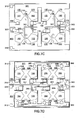
- FIG 3A is an enlarged view showing in more detail part of SBAR 106 incorporating the above-mentioned first embodiment of acoustic decoupler 130.
- acoustic decoupler 130 is composed of a layer 131 of acoustic decoupling material located between the electrode 114 of FBAR 110 and electrode 122 of FBAR 120.
- Layer 131 of acoustic decoupling material additionally extends between the electrode 144 of FBAR 150 and electrode 162 of FBAR 160 to provides the acoustic decoupling layer 170 of SBAR 108.
- independent but similar layers of acoustic decoupling material provide acoustic decouplers 130 and 170, respectively.
- Important properties of the acoustic decoupling material of layer 131 are an acoustic impedance significantly different from, and typically significantly less than that of the materials of FBARs 110, 120, 150 and 160, and a nominal thickness that is an odd integral multiple of one quarter of the wavelength in the acoustic decoupling material of an acoustic wave having a frequency equal to the center frequency of the pass band of acoustically-coupled transformer 100.
- a high electrical resistivity is also desirable.
- a low dielectric permittivity is also desirable.
- the acoustic decoupling material has an acoustic impedance less that of the materials of the FBARs 110, 120, 150 and 160 and substantially greater than that of air.
- the acoustic impedance of a material is the ratio of stress to particle velocity in the material and is measured in Rayleighs, abbreviated as rayl .
- the materials of the FBARs are typically aluminum nitride (AlN) as the material of piezoelectric layers 116, 126, 156 and 166 and molybdenum (Mo) as the material of electrodes 112, 114, 122, 124, 152, 154, 162 and 164.
- the acoustic impedances of the materials of the FBARs are typically greater than 30 Mrayl (35 Mrayl for AlN and 63 Mrayl for Mo) and the acoustic impedance of air is about 1 krayl.
- materials with an acoustic impedance in the range from about 1 Mrayl to about 16 Mrayl work well as the acoustic coupling material of layer 131.
- Figure 4 is a graph showing how the calculated frequency response of thin-film acoustically-coupled transformer 100 depends on the acoustic impedance of the acoustic decoupling material of layer 131 that constitutes the first embodiment of acoustic decouplers 130 and 170.
- the embodiment illustrated has a center frequency of about 1.9 GHz.
- Calculated frequency responses for embodiments in which the acoustic decoupling material of the acoustic decoupler has acoustic impedances of about 4 Mrayl (polyimide ⁇ curve 240), 8 Mrayl (curve 242) and 16 Mrayl (curve 244) are shown.
- the bandwidth of transformer 100 increases with increasing acoustic impedance of the acoustic decoupling material.
- the acoustic impedance is 16 Mrayl
- the resonances of the FBARs are over coupled, which causes the characteristic double peak in the pass band response.
- the thickness of the layer 131 ( Figure 3A) of acoustic decoupling material that constitutes acoustic decouplers 130 and 170 has a nominal thickness equal to one quarter of the wavelength in the acoustic decoupling material of an acoustic wave having a frequency equal to the center frequency of the transformer's pass band, i.e., t ⁇ ⁇ n /4, where t is the thickness of layer 131 and ⁇ n is the wavelength in the acoustic decoupling material of an acoustic wave having a frequency equal to the center frequency of the pass band of transformer 100.
- a thickness of layer 131 within approximately ⁇ 10% of the nominal thickness can alternatively be used. A thickness outside this range can alternatively be used with some degradation in performance. However, the thickness of layer 131 should differ significantly from 0 ⁇ n at one extreme and ⁇ n /2 at the other extreme.
- layer 131 of acoustic decoupling material has a nominal thickness equal to an odd integral multiple of one quarter of the wavelength in the acoustic decoupling material of an acoustic wave having a frequency equal to the center frequency of the pass band of transformer 100, i.e., t ⁇ (2m + 1) ⁇ n /4, where t and ⁇ n are as defined above and m is an integer equal to or greater than zero.
- a thickness of layer 131 that differs from the nominal thickness by approximately ⁇ 10% of ⁇ n /4 can alternatively be used. A thickness tolerance outside this range can be used with some degradation in performance, but the thickness of layer 131'should differ significantly from an integral multiple of ⁇ n /2.
- plastic materials have acoustic impedances in the range stated above and can be applied in layers of uniform thickness in the thickness ranges stated above. Such plastic materials are therefore potentially suitable for use as the acoustic decoupling material of layer 131 that constitutes acoustic decouplers 130 and 170.
- the acoustic decoupling material must also be capable of withstanding the temperatures of the fabrication operations performed after layer 131 has been deposited on electrodes 114 and 154 to form acoustic decouplers 130 and 170.
- electrodes 122, 124 162 and 164 and piezoelectric layers 126 and 166 are deposited by sputtering after layer 131 has been deposited. Temperatures as high as 300 °C are reached during these deposition processes. Thus, a plastic that remains stable at such temperatures is desirable as the acoustic decoupling material of layer 131.
- Plastic materials typically have a very high acoustical attenuation per unit length compared with the other materials of SBARs 106 and 108. However, since the thickness of layer 131 of plastic acoustic decoupling material is typically less than 1 ⁇ m, the acoustic attenuation introduced by acoustic decouplers 130 and 170 is typically negligible.
- polyimide is used as the acoustic decoupling material of layer 131.
- Polyimide is sold under the trademark Kapton® by E.I. du Pont de Nemours and Company.
- acoustic decouplers 130 and 170 are composed of layer 131 of polyimide applied to electrodes 114 and 154 by spin coating, spraying, dipping or another suitable method.
- Polyimide has an acoustic impedance of about 4 Mrayl.
- a poly(para-xylylene) is used as the acoustic decoupling material of layer 131.
- acoustic decouplers 130 and 170 are composed of layer 131 of poly(para-xylylene) applied to electrodes 114 and 154 by vacuum deposition.
- Poly(para-xylylene) is also known in the art as parylene.
- the dimer precursor di-para-xylylene from which parylene is made and equipment for performing vacuum deposition of layers of parylene are available from many suppliers. Parylene has an acoustic impedance of about 1.8 Mrayl.
- the acoustic decoupling material of layer 131 has an acoustic impedance substantially greater than the materials of FBARs 110, 120, 150 and 160. No materials having this property are known at this time, but such materials may become available in future, or lower acoustic impedance FBAR materials may become available in future.
- the thickness of layer 131 of such high acoustic impedance acoustic decoupling material is as described above.
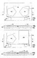
- FIG. 3B is an enlarged view showing in more detail part of SBAR 106 incorporating a second embodiment of acoustic decoupler 130 that incorporates a Bragg structure 161.
- the corresponding part of SBAR 108 incorporating such second embodiment of acoustic decoupler 170 is similar in structure and will not be independently described.
- Bragg structure 161 is composed of a low acoustic impedance Bragg element 163 sandwiched between high acoustic impedance Bragg elements 165 and 167.
- Low acoustic impedance Bragg element 163 is a layer of a low acoustic impedance material whereas high acoustic impedance Bragg elements 165 and 167 are each a layer of high acoustic impedance material.
- the acoustic impedances of the Bragg elements are characterized as "low” and "high” with respect to one another and additionally with respect to the acoustic impedance of the piezoelectric material of piezoelectric elements 116 and 126.
- At least one of the Bragg elements additionally has a low dielectric permittivity.
- at least one of the Bragg elements additionally has a high electrical resistivity to provide electrical insulation between primary and secondary.
- Each of the layers constituting Bragg elements 161, 163 and 165 has a nominal thickness equal to an odd integral multiple of one quarter of the wavelength in the material of the layer of an acoustic wave having a frequency equal to the center frequency of transformer 100.
- Layers that differ from the nominal thickness by approximately ⁇ 10% of one quarter of the wavelength can alternatively be used.
- a thickness tolerance outside this range can be used with some degradation in performance, but the thickness of the layers should differ significantly from an integral multiple of one-half of the wavelength.
- low acoustic impedance Bragg element 163 is a layer of silicon dioxide (SiO 2 ), which has an acoustic impedance of about 13 Mrayl
- each of the high acoustic impedance Bragg elements 165 and 167 is a layer of the same material as electrodes 114 and 122, respectively, i.e., molybdenum, which has an acoustic impedance of about 63 Mrayl.
- high acoustic impedance Bragg elements 165 and 167 and electrodes 114 and 122, respectively, of FBARs 110 and 120, respectively allows high acoustic impedance Bragg elements 165 and 167 additionally to serve as electrodes 114 and 122, respectively.
- high acoustic impedance Bragg elements 165 and 167 have a nominal thickness equal to one quarter of the wavelength in molybdenum of an acoustic wave having a frequency equal to the center frequency of the pass band of transformer 100
- low acoustic impedance Bragg element 163 had a nominal thickness equal to three quarters of the wavelength in SiO 2 of an acoustic wave having a frequency equal to the center frequency of the pass band of the transformer.
- Using a three-quarter wavelength-thick layer of SiO 2 instead of a one-quarter wavelength thick layer of SiO 2 as low acoustic impedance Bragg element 163 reduces the capacitance between FBARs 110 and 120, but reduces the bandwidth of transformer 100.
- Bragg structure 161 may be composed of more than one (e.g., n) low acoustic impedance Bragg elements interleaved with a corresponding number (i.e., n + 1) of high acoustic impedance Bragg elements.
- the Bragg structure may be composed of two low acoustic impedance Bragg element interleaved with three high acoustic impedance Bragg elements. Only one of the Bragg elements need be insulating.
- low acoustic impedance Bragg element 163 additionally extends between the electrodes 154 and 162 of SBAR 108 and provide parts of acoustic decouplers 130 and 170.
- electrodes 154 and 162 have nominal thicknesses equal to one quarter of the wavelength in the electrode material of an acoustic wave having a frequency equal to the center frequency of the pass band of transformer 100.
- acoustic decouplers 130 and 170 may incorporate respective independent but similar low acoustic impedance Bragg elements.
- a wafer (not shown) of single-crystal silicon is provided.
- a portion of the wafer constitutes, for each transformer being fabricated, a substrate corresponding to the substrate 102 of transformer 100.
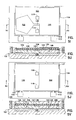
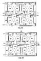
- Figures 5A-5L and Figures 5M-5X illustrate, and the following description describes, the fabrication of transformer 100 in and on a portion of the wafer. As transformer 100 is fabricated, the remaining transformers on the wafer are similarly fabricated.
- cavity 104 The portion of the wafer that constitutes substrate 102 of transformer 100 is selectively wet etched to form cavity 104, as shown in Figures 5A and 5M. Cavity 104 may alternatively be formed by dry etching.
- a layer of fill material (not shown) is deposited on the surface of the wafer with a thickness sufficient to fill the cavities. The surface of the wafer is then planarized to leave the cavity filled with the fill material.
- Figures 5B and 5N show cavity 104 in substrate 102 filled with fill material 105.
- the fill material was phosphosilicate glass (PSG) and was deposited using conventional low-pressure chemical vapor deposition (LPCVD).
- the fill material may alternatively be deposited by sputtering or by spin coating.
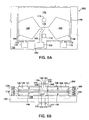
- a layer of metal is deposited on the surface of the wafer and the fill material.
- the metal is patterned to define electrode 112, electrode 152, bonding pad 132 and electrical trace 133 extending between electrode 112 and bonding pad 132, bonding pad 172 and electrical trace 173 extending between electrode 152 and bonding pad 172, as shown in Figures 5C and 50.
- Electrode 112 and electrode 152 are located so that part of the surface of fill material 105 remains exposed to enable the fill material to be removed later by etching, as will be described below.
- Electrode 112 and electrode 152 typically have an irregular shape in a plane parallel to the major surface of wafer 302.
- An irregular shape minimizes lateral modes in the FBARs of which the electrodes form part, as described in United States patent no. 6,215,375 of Larson III et al., the disclosure of which is incorporated herein by reference.
- Electrodes 112, 114, 122, 124, 152, 154, 162 and 164 are formed by patterning metal layers such that, in respective planes parallel to the major surface of the wafer, electrodes 112 and 114 of FBAR 110 have the same shape, size, orientation and position, electrodes 122 and 124 of FBAR 120 have the same shape, size, orientation and position, electrodes 152 and 154 of FBAR 150 have the same shape, size, orientation and position and electrodes 162 and 164 of FBAR 160 have the same shape, size, orientation and position.
- electrodes 114 and 122 additionally have the same shape, size, orientation and position and electrodes 154 and 162 additionally have the same shape, size, orientation and position.
- the metal deposited to form electrode 112, bonding pad 132, trace 133, electrode 152, bonding pad 172 and trace 173 was molybdenum.
- the molybdenum was deposited with a thickness of about 440 nm by sputtering, and was patterned by dry etching to define pentagonal electrodes each with an area of about 7,000 square ⁇ m.
- the area of the electrodes is chosen to provide a given electrical impedance. The impedance also depends on the height of SBARs 106 and 108 and the operating frequency.
- Electrodes 112 and 152 may alternatively be used as the material of electrodes 112 and 152, bonding pads 132 and 172 and traces 133 and 173.
- the electrodes, bonding pads and traces may alternatively comprise layers of more than one material.
- Piezoelectric material is deposited and is patterned to define a piezoelectric layer 117 that provides normal c-axis piezoelectric element 116 of FBAR 110 and reverse c-axis piezoelectric element 156 of FBAR 150.
- the piezoelectric material is deposited by first depositing a thin layer of reverse c-axis piezoelectric material and patterning the thin layer to define seed layer 155 over electrode 152, as shown in Figures 5D and 5P. Then, a thick layer of piezoelectric material having a nominal thickness equal to the design thickness of piezoelectric elements 116 and 156 is deposited and is patterned to define piezoelectric layer 117, as shown in Figures 5E and 5Q.
- Seed layer 155 remains in place under part of layer 117 but is not shown in Figure 5Q due to its negligible thickness compared with layer 117.
- Piezoelectric layer 117 is patterned to expose part of the surface of fill material 105 and bonding pads 132 and 172. Piezoelectric layer 117 is additionally patterned to define windows 119 that provide access to additional parts of the surface of the fill material.
- the thin layer of piezoelectric material that is patterned to define seed layer 155 is deposited under deposition conditions that promote the formation of reverse c-axis piezoelectric material. Patterning the thin layer of piezoelectric material to define seed layer 155 exposes electrode 112, part of the surface of fill material 105, bonding pad 132, electrical trace 173, bonding pad 172 and part of electrical trace 173.
- the thick layer of piezoelectric material is deposited under normal deposition conditions.
- the piezoelectric material of the thick layer grows with the direction of its c-axis reversed in the portion deposited on seed layer 155 but with its c-axis in the normal direction elsewhere.
- Patterning the thick layer of piezoelectric material to define piezoelectric layer 117, which provides piezoelectric element 116 and piezoelectric element 156, exposes part of the surface of fill material 105, bonding pad 132 and part of electrical trace 133, bonding pad 172 and part of electrical trace 173, and additionally forms windows 119 that provide access to additional parts of the surface of the fill material.
- the thin layer of piezoelectric material was aluminum nitride and was deposited with a thickness of about 40 nm by sputtering in an oxygen-rich sputtering environment.
- this deposition process could be used to deposit the entire thickness of piezoelectric layer 117, the resulting piezoelectric material typically has piezoelectric properties inferior to those of piezoelectric material grown under normal growth conditions.
- the reverse c-axis piezoelectric material deposited on the seed layer has piezoelectric properties comparable with those of normal c-axis piezoelectric material.
- depositing layer 117 of piezoelectric material forms piezoelectric element 116 with its c-axis (indicated by arrow 146) in the normal direction and piezoelectric element 156 with its c-axis (indicated by arrow 148) in the reverse direction.
- the thin layer of piezoelectric material was patterned to define seed layer 155 by wet etching in potassium hydroxide or by chlorine-based dry etching.
- the piezoelectric material deposited to form piezoelectric layer 117 was aluminum nitride and was deposited with a thickness of about 760 nm by sputtering.
- the piezoelectric material was patterned by wet etching in potassium hydroxide or by chlorine-based dry etching.
- Alternative materials for piezoelectric layer 117 include zinc oxide, cadmium sulfide and poled ferroelectric materials such as perovskite ferroelectrics including lead zirconium titanate, lead meta niobate and barium titanate. Poling of ferroelectric materials is described below with reference to Figures 7A-7F.
- a layer of metal is deposited and is patterned to define electrode 114, electrode 154 and electrical trace 137 extending between electrode 114 and electrode 154, as shown in Figures 5F and 5R.
- the metal deposited to form electrode 114, electrode 154 and trace 137 was molybdenum.
- the molybdenum was deposited with a thickness of about 440 nm by sputtering, and was patterned by dry etching.
- Other refractory metals may alternatively be used as the material of electrodes 114 and 154 and trace 137.
- the electrodes and trace may alternatively comprise layers of more than one material.
- a layer of acoustic decoupling material is then deposited and is patterned to define an acoustic decoupling layer 131 that provides acoustic decoupler 130 and acoustic decoupler 170, as shown in Figures 5G and 5S.
- Acoustic decoupling layer 131 covers at least electrode 114 and electrode 154 ( Figure 5F), and is patterned to expose part of the surface of fill material 105 and bonding pads 132 and 172. Acoustic decoupling layer 131 is additionally patterned to define windows 119 that provide access to additional parts of the surface of the fill material.
- the acoustic decoupling material was polyimide with a thickness of about 750 nm, i.e., three quarters of a center frequency wavelength of 1.9 GHz in the polyimide.
- the polyimide was deposited to form acoustic decoupling layer 131 by spin coating, and was patterned by photolithography. Polyimide is photosensitive so that no photoresist is needed. As noted above, other plastic materials can be used as the acoustic decoupling material.
- the acoustic decoupling material can be deposited by methods other than spin coating.
- the wafer was baked at about 300 °C before further processing was performed.
- the bake evaporates volatile constituents of the polyimide and prevents the evaporation of such volatile constituents during subsequent processing from causing separation of subsequently-deposited layers.
- a layer of metal is deposited and is patterned to define electrode 122, electrode 162 and electrical trace 138 extending from electrode 122 to electrode 162, as shown in Figures 5H and 5T.
- the metal deposited to form electrodes 122 and 162 and electrical trace 138 was molybdenum.
- the molybdenum was deposited with a thickness of about 440 nm by sputtering, and was patterned by dry etching.
- Other refractory metals may alternatively be used as the material of electrodes 122 and 162 and electrical trace 138.
- the electrodes and trace may alternatively comprise layers of more than one material.
- Piezoelectric material is deposited and is patterned to define a piezoelectric layer 127 that provides normal c-axis piezoelectric element 126 of FBAR 120 and reverse c-axis piezoelectric element 166 of FBAR 160.
- the piezoelectric material is deposited by first depositing a thin layer of reverse c-axis piezoelectric material and patterning the thin layer to define a seed layer 165 over electrode 162, as shown in Figures 51 and 5U. Then, a thick layer of piezoelectric material having a nominal thickness equal to the design thickness of piezoelectric elements 126 and 166 is deposited and is patterned to define piezoelectric layer 127, as shown in Figures 5J and 5V.
- Seed layer 165 remains in place under part of layer 127 but is not shown in Figure 5V due to its negligible thickness compared with layer 127.
- Piezoelectric layer 127 is patterned to expose part of the surface of fill material 105 and bonding pads 132 and 172. Piezoelectric layer 127 is additionally patterned to define windows 119 that provide access to additional parts of the surface of the fill material.
- the thin layer of piezoelectric material that is patterned to define seed layer 165 is deposited under deposition conditions that promote the formation of reverse c-axis piezoelectric material. Patterning the thin layer of piezoelectric material to define seed layer 165 exposes electrode 122, part of the surface of fill material 105, bonding pad 132, part of electrical trace 133, part of electrical trace 138 adjacent electrode 122, bonding pad 172 and part of electrical trace 173.
- the thick layer of piezoelectric material is deposited under normal deposition conditions.
- the piezoelectric material of the thick layer grows with the direction of its c-axis reversed in the portion deposited on seed layer 165 but with its c-axis in the normal direction elsewhere.
- Patterning the thick layer of piezoelectric material to define piezoelectric layer 127 which provides piezoelectric element 126 and piezoelectric element 166, exposes part of the surface of fill material 105, bonding pad 132 and part of electrical trace 133, bonding pad 172 and part of electrical trace 173, and additionally forms windows 119 that provide access to additional parts of the surface of the fill material.
- the thin layer of piezoelectric material was aluminum nitride and was deposited with a thickness of about 40 nm by sputtering in an oxygen-rich sputtering environment.
- this deposition process could be used to deposit the entire thickness of piezoelectric layer 127, as described above.
- the thin layer of piezoelectric material was patterned to define seed layer 165 by wet etching in potassium hydroxide or by chlorine-based dry etching.
- the piezoelectric material deposited to form piezoelectric layer 127 was aluminum nitride and was deposited with a thickness of about 760 nm by sputtering.
- the piezoelectric material was patterned by wet etching in potassium hydroxide or by chlorine-based dry etching.
- Alternative materials for piezoelectric layer 127 include zinc oxide, cadmium sulfide and poled ferroelectric materials such as perovskite ferroelectric materials including lead zirconium titanate, lead meta niobate and barium titanate. Poling of ferroelectric materials is described below with reference to Figures 7A-7F.
- a layer of metal is deposited and is patterned to define electrode 124, electrode 164, bonding pad 134, electrical trace 135 extending from electrode 124 to bonding pad 134, bonding pad 174 and electrical trace 175 extending from electrode 164 to bonding pad 174, as shown in Figures 5K and 5W.
- the metal deposited to form electrodes 124 and 164, bonding pads 134 and 174 and electrical traces 135 and 175 was molybdenum.
- the molybdenum was deposited with a thickness of about 440 nm by sputtering, and was patterned by dry etching.
- Other refractory metals such may alternatively be used as the material of electrodes 124 and 164, bonding pads 134 and 174 and electrical traces 135 and 175.
- the electrodes, bonding pads and traces may alternatively comprise layers of more than one material.
- a gold protective layer (not shown) is then deposited on the exposed surfaces of bonding pads 132, 134, 172 and 174.
- the wafer is then isotropically wet etched to remove fill material 105 from cavity 104. As noted above, portions of the surface of fill material 105 remain exposed through, for example, windows 119. The etch process leaves thin-film acoustically-coupled transformer 100 suspended over cavity 104, as shown in Figures 5L and 5X.
- the etchant used to remove fill material 105 was dilute hydrofluoric acid.
- the wafer is then divided into individual thin-film acoustically-coupled transformers, including transformer 100.
- transformer 100 Each transformer is then mounted in a package and electrical connections are made between bonding pads 132, 172, 134 and 174 of the transformer and pads that are part of the package.
- bonding pad 172 electrically connected to electrode 124 and bonding pad 174 electrically connected to electrode 154 provide the second terminals of transformer 100.
- the first terminals provide the primary terminals and the second terminals provide the secondary terminals of thin-film acoustically-coupled transformer 100.
- the first terminals provide the secondary terminals and the second terminals provide the primary terminals of thin-film acoustically-coupled transformer 100.
- reverse c-axis piezoelectric material constitute piezoelectric element 156 of FBAR 150 and piezoelectric element 166 of FBAR 160.
- a layer of metal is deposited and is patterned in a manner similar to that shown in Figures 5F and 5Q to define high acoustic impedance Bragg elements incorporating electrodes 114 and 154, respectively, and additionally to define electrical trace 137 extending between the electrodes.
- the high acoustic impedance Bragg elements are each similar to high acoustic impedance Bragg element 165 shown in Figure 3B.
- the layer of metal is deposited with a nominal thickness equal to an odd, integral multiple of one quarter of the wavelength in the metal of an acoustic wave having a frequency equal to the center frequency of the pass band of transformer 100.
- the metal deposited to form the high acoustic impedance Bragg elements respectively incorporating electrodes 114 and 154 is molybdenum.
- the molybdenum is deposited with a thickness of about 820 nm (one-quarter wavelength in Mo at about 1.9 GHz) by sputtering, and is patterned by dry etching.
- Other refractory metals may alternatively be used as the material of the high acoustic impedance Bragg elements respectively incorporating electrodes 114 and 154.
- the high acoustic impedance Bragg elements may alternatively comprise layers of more than one metal.
- a layer of low acoustic impedance material is then deposited and is patterned in a manner similar to that shown in Figures 5G and 5S to define a low acoustic impedance Bragg element.
- the layer of low acoustic impedance material is deposited with a nominal thickness equal to an odd, integral multiple of one quarter of the wavelength in the low acoustic impedance material of an acoustic wave having a frequency equal to the center frequency of the pass band of transformer 100.
- the low acoustic impedance Bragg element covers at least the high acoustic impedance Bragg elements, and is additionally patterned to expose part of the surface of fill material 105 and bonding pads 132 and 172.
- the layer of low acoustic impedance material is additionally patterned to define windows 119 that provide access to additional parts of the surface of the fill material.
- the low acoustic impedance material is SiO 2 with a thickness of about 790 nm.
- the SiO 2 is deposited by sputtering, and is patterned by etching.
- Other low acoustic impedance material that can be used as the material of low acoustic impedance Bragg element include phosphosilicate glass (PSG), titanium dioxide and magnesium fluoride.
- PSG phosphosilicate glass
- titanium dioxide titanium dioxide
- magnesium fluoride magnesium fluoride
- a layer of metal is deposited and is patterned in a manner similar to that shown in Figures 5H and 5T to define high acoustic impedance Bragg elements respectively incorporating electrodes 122 and 162.
- the layer of metal is additionally patterned to define an electrical trace 138 extending from electrode 122 to electrode 162.
- the layer of metal is deposited with a nominal thickness equal to an odd, integral multiple of one quarter of the wavelength in the metal of an acoustic wave having a frequency equal to the center frequency of the pass band of transformer 100.
- the metal deposited to form a high acoustic impedance Bragg elements respectively incorporating electrodes 122 and 162 is molybdenum.
- the molybdenum is deposited with a thickness of about 820 nm (one-quarter wavelength in Mo) by sputtering, and is patterned by dry etching.
- Other refractory metals may alternatively be used as the material of the high acoustic impedance Bragg elements respectively incorporating electrodes 122 and 162 and electrical trace 138.
- the high acoustic impedance Bragg elements, pads and electrical traces may alternatively comprise layers of more than one material.
- one or both of electrical circuits 141 and 142 has an additional center tap terminal.
- Figure 6A shows a second embodiment 200 of a thin-film acoustically-coupled transformer in accordance with the invention part-way through its fabrication.
- electrical circuit 142 has a center tap terminal.
- Elements of thin-film acoustically-coupled transformer 200 that correspond to elements of thin-film acoustically-coupled transformer 100 described above with reference to Figures 1A-1C and 2 are indicated by the same reference numerals and will not be described again in detail.
- FIG. 6A shows thin-film acoustically-coupled transformer 200 at the stage of its fabrication corresponding to that described above with reference to Figures 5H and 5T.
- piezoelectric layer 117 and layer 131 of acoustic decoupling material are patterned additionally to define a support region 186.
- a metal layer is deposited and is patterned to define electrode 122, electrode 162 and electrical trace 138 extending between electrodes 122 and 162, as described above.
- the metal layer is additionally patterned to define a bonding pad 182 and an electrical trace 183 extending between electrical trace 138 and bonding pad 182. Bonding pad 182 is located on support region 186 and provides the center tap terminal of electrical circuit 241.
- the metal deposited was molybdenum with a thickness of about 440 nm.
- the metal was deposited by sputtering and was patterned by dry etching. Other refractory metals may alternatively be used.
- Electrodes 122 and 162, electrical traces 138 and 183 and bonding pad 182 may alternatively comprise layers of more than one material.
- Fabrication of thin-film acoustically-coupled transformer 200 is completed substantially as described above with reference to Figures 5I, 5U, 5J, 5V, 5K, 5W, 5L and 5X, except that piezoelectric layer 127 is additionally patterned to expose bonding pad 182.
- FIG. 6B is a schematic drawing of the electrical circuits of acoustically-coupled transformer 200.
- First electrical circuit 141 is described above.
- a second electrical circuit 242 is composed of electrical trace 138 that electrically connects electrode 122 of upper FBAR 120 of SBAR 106 to electrode 162 of upper FBAR 160 of SBAR 108.
- Second electrical circuit 242 is additionally composed of electrical trace 135 that electrically connects electrode 124 to terminal 134, electrical trace 175 that electrically connects electrode 164 to terminal 174, and electrical trace 183 that connects electrical trace 138 to terminal 182.
- electrical circuit 242 electrically connects the upper FBARs in series and provides a center tap connection.
- a bonding pad similar to bonding pad 182 and an electrical trace similar to trace 183 but connecting to trace 137 may additionally or alternatively be defined in the metal layer deposited and patterned in the process described above with reference to Figures 5F and 5R to provide a center tap terminal in electrical circuit 141 ( Figure 6B).
- a layer of piezoelectric material having a thickness equal to the design thickness of piezoelectric element 116 ( Figure 2) is then deposited under deposition conditions that promote the formation of normal c-axis material.
- the normal c-axis piezoelectric material is then patterned to define piezoelectric element 116.
- the patterning exposes electrode 152, bonding pad 132, part of electrical trace 133, bonding pad 172, electrical trace 173 and additionally defines windows 119 that provide access to additional parts of the surface of the fill material.
- Piezoelectric element 116 is then covered with a suitable etch stop layer, such as a layer of molybdenum.
- a layer of piezoelectric material having a thickness equal to the design thickness of piezoelectric element 156 ( Figure 2) is then deposited under deposition conditions that promote the formation of reverse c-axis material.
- the reverse c-axis material is then patterned by photolithographically-defined etching to define piezoelectric element 156.
- the patterning exposes piezoelectric element 116, and additionally exposes part of the surface of fill material 105 and bonding pads 132 and 172.
- the etch stop layer protects piezoelectric element 116 during the patterning of the layer of reverse c-axis material to define piezoelectric element 156.
- the etch stop layer is then removed.
- Fabrication of the transformer continues by performing the processes described above with reference to Figures 5F-5H and 5R-5T. A process similar to that just described is then used to form piezoelectric element 126 of normal c-axis material and piezoelectric element 166 of reverse c-axis material shown in Figure 5J. Piezoelectric elements 126 and 166 may alternatively be formed in other ways. Fabrication of the transformer is then completed by performing the processes described above with reference to Figures 5K and 5L, and 5W and 5X.
- a layer of piezoelectric material having a thickness equal to the design thickness of piezoelectric element 116 is then deposited under deposition conditions that promote the formation of normal c-axis material.
- the normal c-axis material is then patterned to define piezoelectric element 116.
- the patterning exposes electrode 152, bonding pad 132, part of electrical trace 133, bonding pad 172 and electrical trace 173 and additionally defines windows 119 that provide access to additional parts of the surface of the fill material.
- a layer of photoresist or other protective material is deposited and is patterned to define a window similar in shape and extent to seed layer 155 shown in Figure 5D. Electrode 152 is exposed through the window.
- a layer of reverse c-axis piezoelectric material having a thickness equal to the design thickness of piezoelectric element 156 is then deposited under deposition conditions that promote the formation of reverse c-axis material.
- the layer of reverse c-axis piezoelectric material is then patterned using a lift-off process to define piezoelectric element 156.
- the lift-off process removes all the reverse c-axis material deposited on the photoresist but leaves reverse c-axis material deposited in the window defined in the photoresist. The photoresist is then removed.
- Fabrication of the transformer continues by performing the processes described above with reference to 5F-5H and 5R-5T. A process similar to that just described is then used to form piezoelectric element 126 of normal c-axis material and piezoelectric element 166 of reverse c-axis material shown in Figure 5J. Piezoelectric elements 126 and 166 may alternatively be formed in other ways. Fabrication of the transformer is then completed by performing the processes described above with reference to Figures 5K and 5L, and 5W and 5X.
- the normal c-axis piezoelectric material and the reverse c-axis piezoelectric material may be deposited in a reverse order to that just described.
- FIGS 7A-7F illustrate an exemplary embodiment of a method of making an embodiment 300 of a thin-film acoustically-coupled transformer in accordance with the invention in which the piezoelectric elements each comprise a layer of a poled ferroelectric material.
- Elements of thin-film acoustically-coupled transformer 300 that correspond to elements of thin-film acoustically-coupled transformer 100 described above with reference to Figures 1A-1C and 2 are indicated by the same reference numerals and will not be described again in detail.
- the piezoelectric material of piezoelectric layers 117 and 127 is a poled ferroelectric material.
- the portion of piezoelectric layer 117 that constitutes piezoelectric element 116 is poled in the normal direction whereas the portion of piezoelectric layer 117 that constitutes piezoelectric element 156 is poled in the reverse direction.
- the portion of piezoelectric layer 127 that constitutes piezoelectric element 126 is poled in the normal direction whereas the portion of piezoelectric layer 127 that constitutes piezoelectric element 166 is poled in the reverse direction.
- the opposite poling of the portions of the piezoelectric layers is imposed by applying electric fields in opposite directions to the respective portions.
- Figures 7A-7F are plan views illustrating the processing of a wafer 302 to fabricate exemplary embodiments of thin-film acoustically-coupled transformers 300 similar to thin-film acoustically-coupled transformer 100 described above with referenced to Figures 1A-1C.
- thousands of thin-film acoustically-coupled transformers are typically fabricated on a single wafer.
- the number of thin-film acoustically-coupled transformers shown in Figures 7A-7F has been reduced to four to simplify the drawing.
- the quantitative examples set forth below relate to an embodiment of thin-film acoustically-coupled transformer 300 suitable for operation at a frequency of about 1.9 GHz. Embodiments suitable for operation at other frequencies will differ in such details.
- a first metal layer is deposited on the wafer.
- the material of piezoelectric layer 317 ( Figure 7B) is a perovskite ferroelectric such as lead zirconium titanate (PZT)
- the material of the first metal layer is platinum or iridium. These materials are compatible with the deposition process later used to deposit piezoelectric layer 317.
- the material of the first metal layer is a refractory metal, such as molybdenum, coated with a thin protective layer of platinum or iridium.
- the layer of refractory metal has a thickness that differs from the design thickness of the first metal layer by the thickness of the protective layer.
- the protective layer provides the above-mentioned deposition process compatibility.
- the first metal layer is patterned to define electrodes 112 and 152, bonding pad 132, electrical trace 133, bonding pad 172 and electrical trace 173 all located on fill material 105, as shown in Figure 7A and as described above with reference to Figures 5C and 50.
- the first metal layer is also patterned to define level 1 normal busses 311, a level 1 normal contact pad 313 at one end of each of busses 311 and an electrical trace 315 that extends from the electrode 112 of each transformer 300 to an adjacent one of level 1 normal busses 311.
- the first metal layer is additionally patterned to define level 1 reverse bus 321, a level 1 reverse contact pad 323 at one end of bus 321 and an electrical trace 325 that extends from the bonding pad 172 of each transformer 300 to level 1 reverse bus 321.
- a first layer of ferroelectric material is then deposited and is patterned to define piezoelectric layer 317 that provides piezoelectric element 116 and piezoelectric element 156, as shown in Figure 7B.
- Piezoelectric layer covers at least electrode 112 and 152 ( Figure 7A) and additionally covers level 1 busses 311 and 321.
- the patterning exposes part of the surface of fill material 105, bonding pads 132 and 172, level 1 normal contact pad 313 and level 1 reverse contact pad 323, and additionally defines windows 119.
- the ferroelectric material deposited and patterned to define piezoelectric layer 317 was lead zirconium titanate (PZT) and was deposited with a thickness of about 500 nm by a process such as RF sputtering, sol gel or metal-organic chemical vapor deposition (MOCVD).
- the ferroelectric material was patterned by wet etching or chlorine-based dry etching.
- Alternative ferroelectric materials include perovskite ferroelectric materials, such as lead meta niobate and barium titanate.
- a second metal layer is deposited.
- the material of piezoelectric layer 327 ( Figure 7D) is a perovskite ferroelectric material such as lead zirconium titanate (PZT)
- the material of the second metal layer is platinum or iridium. These materials are compatible with the deposition process later used to deposit piezoelectric layer 327.
- the second metal layer is composed of a thin protective layer of platinum or iridium molybdenum adjacent piezoelectric layer 317 and a layer of a refractory metal such as molybdenum.
- the layer of refractory metal has a thickness that differs from the design thickness of the second metal layer by the thickness of the protective layer.
- the protective layer provides the above-mentioned deposition process compatibility.
- the second metal layer and is patterned to define electrode 114, electrode 154 and electrical trace 137 as described above with reference to Figures 5F and 5R and as shown in Figure 7B.
- the second metal layer is additionally patterned to define a level 2 bus 331, a level 2 contact pad 333 at one end of bus 331 and an electrical trace 335 that extends from the electrical trace 137 of each transformer 300 to level 2 bus 331.
- a layer of acoustic decoupling material is then deposited and is patterned to define an acoustic decoupling layer 331 that provides acoustic decoupler 130 and acoustic decoupler 170, as described above with reference to Figures 5G and 5S, and as shown in Figure 7C.
- Acoustic decoupling layer 331 covers electrode 114 and electrode 154 ( Figure 7B) and additionally covers level 2 bus 331.
- the patterning exposes part of the surface of fill material 105, bonding pads 132 and 172, level 1 contact pads 313 and 323 and level 2 contact pad 333, and additionally defines windows 119.
- a third metal layer is deposited on the wafer.
- the material of piezoelectric layer 327 ( Figure 7D) is a perovskite ferroelectric material such as lead zirconium titanate (PZT)
- the material of the third metal layer is platinum or iridium. These materials are compatible with the deposition process later used to deposit piezoelectric layer 327.
- the third metal layer is composed of a layer of a refractory metal, such as molybdenum, coated with a thin protective layer of platinum or iridium.
- the layer of refractory metal has a thickness that differs from the design thickness of the third metal layer by the thickness of the protective layer.
- the protective layer provides the above-mentioned deposition process compatibility.
- the third metal layer is patterned to define electrode 122, electrode 162 and electrical trace 138, as described above with reference to Figures 5H and 5T, and as shown in Figure 7C.
- the third metal layer is additionally patterned to define a level 3 bus 341, a level 3 contact pad 343 at one end of bus 341 and an electrical trace 194 that extends from the electrical trace 138 of each transformer 300 to level 3 bus 341.
- a second layer of ferroelectric material is then deposited on the wafer and is patterned to define piezoelectric layer 327 that provides piezoelectric elements 126 and 166, as shown in Figure 7D.
- Piezoelectric layer 327 covers electrodes 122 and 162 and additionally covers level 3 bus 341.
- the patterning exposes part of the surface of fill material 105, bonding pads 132 and 172, level 1 contact pads 313 and 323, level 2 contact pad 333 and level 3 contact pad 343, and additionally defines windows 119.
- the ferroelectric material deposited and patterned to form piezoelectric layer 327 was PZT and was deposited with a thickness of about 500 nm by a process such as RF sputtering, sol gel or metal-organic chemical vapor deposition (MOCVD).
- the ferroelectric material was patterned by wet etching or by chlorine-based dry etching.
- Alternative ferroelectric materials include perovskite ferroelectric materials such as lead meta niobate and barium titanate.
- a fourth metal layer is deposited.
- the material of the fourth metal layer is a refractory metal such as molybdenum.
- a refractory metal can be used as the material of the fourth metal layer because no perovskite ferroelectric material deposition process is performed after the fourth metal layer is deposited.
- the fourth metal layer is patterned to define electrode 124, electrode 164, bonding pad 134, electrical trace 135, bonding pad 174 and electrical trace 175, as described above with reference to Figures 5H and 5T and as shown in Figure 7D.
- the fourth metal layer is additionally patterned to define a level 4 normal bus 351, a level 4 normal contact pad 353 at one end of bus 351 and an electrical trace 355 that extends from the electrode 124 of each transformer 300 to level 4 normal bus 351.
- the fourth metal layer is additionally patterned to define level 4 reverse busses 361, a level 4 reverse contact pad 363 at the end of each bus 361 and an electrical trace 365 that extends from the bonding pad 174 of each transformer 300 to the adjacent reverse level 4 bus 361, as shown in Figure 7D.
- the above-described metal layers were formed by depositing molybdenum with a thickness of about 440 nm by sputtering, and were patterned by dry etching. Alternatives similar to those described above are possible.
- wafer 302 is heated to a temperature of about 125°C and poling voltages are applied to the contact pads as follows: level 2 contact pad 333 and level 3 contact pad 343 are grounded, level 1 normal contact pads 313 and level 4 reverse contact pads 363 are connected to a negative poling voltage, and level 1 reverse contact pad 323 and level 4 normal contact pad 353 are connected to a positive poling voltage.
- This arrangement of poling voltages is applied via busses 311, 321, 331, 341, 351 and 361 and traces 315, 325, 335, 345, 355 and 365 to electrodes 112, 114, 122, 124, 152, 154, 162 and 164.
- the electrodes apply a poling electric field directed away from wafer 302 across the piezoelectric elements of FBARs 110 and 120 ( Figure 2), and apply a poling electric field directed towards wafer 302 across the piezoelectric elements of FBARs 150 and 160 ( Figure 2).
- the poling electric fields set the c-axes of the piezoelectric element 156 of FBAR 150 and piezoelectric element 166 of FBAR 160 opposite in direction to the c-axes of the piezoelectric element 116 of FBAR 110 and the piezoelectric element 126 of FBAR 120.
- poling voltages of polarities inverse to those indicated are applied to the contact pads to set the directions of the c-axes of the piezoelectric elements opposite to those shown in Figure 2.
- poling voltages of polarities opposite those indicated in Figure 7E are applied to contact pads 353 and 363 to set the c-axis of piezoelectric element 166 opposite in direction to the c-axis of piezoelectric element 156 and to set the c-axis of piezoelectric element 126 opposite in direction to the c-axis of piezoelectric element 116.
- poling voltages may be used to set the c-axes of the piezoelectric elements of the lower FBARs opposite in direction to one another and to set the c-axes of the piezoelectric elements of the upper FBARs opposite in direction to one another.
- the poling voltages are in the range from about 250 mV to about 1 V.
- piezoelectric elements 116, 126, 156 and 166 having a thickness of about 500 nm, as described above, poling voltages in this range apply a poling electric field in the range from about 250 kV/m to about 1 MV/m to the piezoelectric elements.
- Wafer 300 is then divided into individual thin-film acoustically-coupled transformers by a known singulation process that removes the regions of wafer 302 indicated by broken line pairs 305 and 306 shown in Figure 7F.
- the singulation process additionally separates traces 315, 325, 335, 345, 355 and 365 ( Figures 7A-7D) from busses 311, 321, 331, 341, 351 and 361. This breaks the electrical connections between the electrodes formerly interconnected by the traces and busses.
- electrical circuits 141 and 142 may be configured to interconnect the lower FBARs and the upper FBARs, respectively, differently from the above-described example.
- the electrical circuits 141 and 142 may electrically connect the lower FBARs and the upper FBARs, respectively, in any one of a parallel, a series, an anti-parallel and an anti-series configuration.
- the parallel, series, anti-parallel and anti-series electrical circuit configurations only eight produce a working transformer.
- the combination of electrical circuit configurations connecting the FBARs determines the impedance and impedance transformation ratio of the transformer, i.e., 1:1 low impedance, 1:1 high impedance, 1:4 or 4:1, and whether the transformer is electrically balanced or electrically unbalanced.
- the row captions indicate the configuration of one of the electrical circuits, e.g., electrical circuit 141
- the column captions indicate the configuration of the other of the electrical circuits, e.g., electrical circuit 142
- B denotes that the transformer is electrically balanced
- X denotes a non-functioning transformer.
- the impedance transformation ratio shown is the impedance transformation from electrical terminals connected to the electrical circuit indicated by the row caption to electrical terminals connected to the electrical circuit indicated by the column caption.
- LOW denotes that the transformer has a low impedance, equivalent to that of two FBARs in parallel
- HI indicates that the transformer has a high impedance, equivalent to that of two FBARs in series.
- Electrodes connected in parallel or in anti-series have in-phase voltages on them whereas electrodes connected in series or in anti-parallel have antiphase voltages on them.
Applications Claiming Priority (4)
| Application Number | Priority Date | Filing Date | Title |
|---|---|---|---|
| US699481 | 2003-10-30 | ||
| US10/699,481 US6946928B2 (en) | 2003-10-30 | 2003-10-30 | Thin-film acoustically-coupled transformer |
| US10/836,663 US7091649B2 (en) | 2003-10-30 | 2004-04-29 | Film acoustically-coupled transformers with two reverse c-axis piezoelectric elements |
| US836663 | 2004-04-29 |
Publications (2)
| Publication Number | Publication Date |
|---|---|
| EP1528677A1 true EP1528677A1 (fr) | 2005-05-04 |
| EP1528677B1 EP1528677B1 (fr) | 2006-05-10 |
Family
ID=34426391
Family Applications (1)
| Application Number | Title | Priority Date | Filing Date |
|---|---|---|---|
| EP04015552A Expired - Fee Related EP1528677B1 (fr) | 2003-10-30 | 2004-07-01 | Transformateur à couplage acoustique de couches minces avec deux éléments piézoélectriques à axe-c inversé |
Country Status (4)
| Country | Link |
|---|---|
| US (1) | US7367095B2 (fr) |
| EP (1) | EP1528677B1 (fr) |
| JP (1) | JP4754803B2 (fr) |
| DE (1) | DE602004000851T2 (fr) |
Cited By (6)
| Publication number | Priority date | Publication date | Assignee | Title |
|---|---|---|---|---|
| GB2431532A (en) * | 2005-10-18 | 2007-04-25 | Avago Technologies General Ip | Film acoustically-coupled transformer (FACT) composed of DSBARs and used as an acoustically-coupled electrical/galvanic isolator |
| WO2008009274A1 (fr) * | 2006-07-17 | 2008-01-24 | Epcos Ag | Circuit avec résonateurs baw |
| GB2445383A (en) * | 2005-10-18 | 2008-07-09 | Avago Technologies General Ip | DSBAR used as an acoustic galvanic isolator |
| GB2425417B (en) * | 2005-04-18 | 2009-08-12 | Agilent Technologies Inc | Acoustically coupled resonators and method of making the same |
| US9859205B2 (en) | 2011-01-31 | 2018-01-02 | Avago Technologies General Ip (Singapore) Pte. Ltd. | Semiconductor device having an airbridge and method of fabricating the same |
| CN107689781A (zh) * | 2016-08-03 | 2018-02-13 | 三星电机株式会社 | 体声波谐振器、滤波器和体声波谐振器的制造方法 |
Families Citing this family (69)
| Publication number | Priority date | Publication date | Assignee | Title |
|---|---|---|---|---|
| US7275292B2 (en) | 2003-03-07 | 2007-10-02 | Avago Technologies Wireless Ip (Singapore) Pte. Ltd. | Method for fabricating an acoustical resonator on a substrate |
| EP1528676B1 (fr) * | 2003-10-30 | 2006-09-13 | Avago Technologies General IP (Singapore) Pte. Ltd | Transformateur à couplage acoustique de couches minces avec matériel piézoélectrique à axe-c inversée |
| US7388454B2 (en) | 2004-10-01 | 2008-06-17 | Avago Technologies Wireless Ip Pte Ltd | Acoustic resonator performance enhancement using alternating frame structure |
| US8981876B2 (en) | 2004-11-15 | 2015-03-17 | Avago Technologies General Ip (Singapore) Pte. Ltd. | Piezoelectric resonator structures and electrical filters having frame elements |
| US7202560B2 (en) | 2004-12-15 | 2007-04-10 | Avago Technologies Wireless Ip (Singapore) Pte. Ltd. | Wafer bonding of micro-electro mechanical systems to active circuitry |
| US7791434B2 (en) | 2004-12-22 | 2010-09-07 | Avago Technologies Wireless Ip (Singapore) Pte. Ltd. | Acoustic resonator performance enhancement using selective metal etch and having a trench in the piezoelectric |
| US7369013B2 (en) | 2005-04-06 | 2008-05-06 | Avago Technologies Wireless Ip Pte Ltd | Acoustic resonator performance enhancement using filled recessed region |
| US7868522B2 (en) | 2005-09-09 | 2011-01-11 | Avago Technologies Wireless Ip (Singapore) Pte. Ltd. | Adjusted frequency temperature coefficient resonator |
| US7737807B2 (en) | 2005-10-18 | 2010-06-15 | Avago Technologies Wireless Ip (Singapore) Pte. Ltd. | Acoustic galvanic isolator incorporating series-connected decoupled stacked bulk acoustic resonators |
| US7463499B2 (en) | 2005-10-31 | 2008-12-09 | Avago Technologies General Ip (Singapore) Pte Ltd. | AC-DC power converter |
| US7586392B2 (en) * | 2006-01-23 | 2009-09-08 | Avago Technologies General Ip (Singapore) Pte. Ltd. | Dual path acoustic data coupling system and method |
| US20070210748A1 (en) * | 2006-03-09 | 2007-09-13 | Mark Unkrich | Power supply and electronic device having integrated power supply |
| US7746677B2 (en) | 2006-03-09 | 2010-06-29 | Avago Technologies Wireless Ip (Singapore) Pte. Ltd. | AC-DC converter circuit and power supply |
| US7479685B2 (en) | 2006-03-10 | 2009-01-20 | Avago Technologies General Ip (Singapore) Pte. Ltd. | Electronic device on substrate with cavity and mitigated parasitic leakage path |
| US8925163B2 (en) | 2006-09-18 | 2015-01-06 | Teknologian Tutkimuskeskus Vtt | Method of manufacturing laterally coupled BAW thin films |
| FI121722B (fi) * | 2006-09-18 | 2011-03-15 | Valtion Teknillinen | Levykondensaattori- tai levyresonaattorijärjestely |
| US20090079514A1 (en) * | 2007-09-24 | 2009-03-26 | Tiberiu Jamneala | Hybrid acoustic resonator-based filters |
| US7791435B2 (en) | 2007-09-28 | 2010-09-07 | Avago Technologies Wireless Ip (Singapore) Pte. Ltd. | Single stack coupled resonators having differential output |
| US7855618B2 (en) | 2008-04-30 | 2010-12-21 | Avago Technologies Wireless Ip (Singapore) Pte. Ltd. | Bulk acoustic resonator electrical impedance transformers |
| US7732977B2 (en) | 2008-04-30 | 2010-06-08 | Avago Technologies Wireless Ip (Singapore) | Transceiver circuit for film bulk acoustic resonator (FBAR) transducers |
| JP5220503B2 (ja) | 2008-07-23 | 2013-06-26 | 太陽誘電株式会社 | 弾性波デバイス |
| US8291559B2 (en) * | 2009-02-24 | 2012-10-23 | Epcos Ag | Process for adapting resonance frequency of a BAW resonator |
| US9255912B2 (en) | 2009-04-29 | 2016-02-09 | The Trustees Of Columbia University In The City Of New York | Monolithic FBAR-CMOS structure such as for mass sensing |
| WO2010127122A1 (fr) * | 2009-04-29 | 2010-11-04 | The Trustees Of Columbia University In The City Of New York | Structure fbar-cmos monolithique telle que pour une détection de masse |
| US20100314973A1 (en) * | 2009-06-10 | 2010-12-16 | Ritek Corporation | Piezoelectric Device with Magnetically Enhanced Piezoelectricity |
| US8902023B2 (en) | 2009-06-24 | 2014-12-02 | Avago Technologies General Ip (Singapore) Pte. Ltd. | Acoustic resonator structure having an electrode with a cantilevered portion |
| US8248185B2 (en) | 2009-06-24 | 2012-08-21 | Avago Technologies Wireless Ip (Singapore) Pte. Ltd. | Acoustic resonator structure comprising a bridge |
| US9847768B2 (en) * | 2009-11-23 | 2017-12-19 | Avago Technologies General Ip (Singapore) Pte. Ltd. | Polarity determining seed layer and method of fabricating piezoelectric materials with specific C-axis |
| US8193877B2 (en) | 2009-11-30 | 2012-06-05 | Avago Technologies Wireless Ip (Singapore) Pte. Ltd. | Duplexer with negative phase shifting circuit |
| US8796904B2 (en) | 2011-10-31 | 2014-08-05 | Avago Technologies General Ip (Singapore) Pte. Ltd. | Bulk acoustic resonator comprising piezoelectric layer and inverse piezoelectric layer |
| US9679765B2 (en) * | 2010-01-22 | 2017-06-13 | Avago Technologies General Ip (Singapore) Pte. Ltd. | Method of fabricating rare-earth doped piezoelectric material with various amounts of dopants and a selected C-axis orientation |
| US9243316B2 (en) | 2010-01-22 | 2016-01-26 | Avago Technologies General Ip (Singapore) Pte. Ltd. | Method of fabricating piezoelectric material with selected c-axis orientation |
| US9842983B2 (en) * | 2010-10-07 | 2017-12-12 | Epcos Ag | Piezoelectric multi-layer component |
| US9203374B2 (en) | 2011-02-28 | 2015-12-01 | Avago Technologies General Ip (Singapore) Pte. Ltd. | Film bulk acoustic resonator comprising a bridge |
| US9048812B2 (en) | 2011-02-28 | 2015-06-02 | Avago Technologies General Ip (Singapore) Pte. Ltd. | Bulk acoustic wave resonator comprising bridge formed within piezoelectric layer |
| US9148117B2 (en) | 2011-02-28 | 2015-09-29 | Avago Technologies General Ip (Singapore) Pte. Ltd. | Coupled resonator filter comprising a bridge and frame elements |
| US9083302B2 (en) | 2011-02-28 | 2015-07-14 | Avago Technologies General Ip (Singapore) Pte. Ltd. | Stacked bulk acoustic resonator comprising a bridge and an acoustic reflector along a perimeter of the resonator |
| US9136818B2 (en) | 2011-02-28 | 2015-09-15 | Avago Technologies General Ip (Singapore) Pte. Ltd. | Stacked acoustic resonator comprising a bridge |
| US9425764B2 (en) | 2012-10-25 | 2016-08-23 | Avago Technologies General Ip (Singapore) Pte. Ltd. | Accoustic resonator having composite electrodes with integrated lateral features |
| US9154112B2 (en) | 2011-02-28 | 2015-10-06 | Avago Technologies General Ip (Singapore) Pte. Ltd. | Coupled resonator filter comprising a bridge |
| US8575820B2 (en) | 2011-03-29 | 2013-11-05 | Avago Technologies General Ip (Singapore) Pte. Ltd. | Stacked bulk acoustic resonator |
| US9444426B2 (en) | 2012-10-25 | 2016-09-13 | Avago Technologies General Ip (Singapore) Pte. Ltd. | Accoustic resonator having integrated lateral feature and temperature compensation feature |
| US9490771B2 (en) | 2012-10-29 | 2016-11-08 | Avago Technologies General Ip (Singapore) Pte. Ltd. | Acoustic resonator comprising collar and frame |
| US9490418B2 (en) | 2011-03-29 | 2016-11-08 | Avago Technologies General Ip (Singapore) Pte. Ltd. | Acoustic resonator comprising collar and acoustic reflector with temperature compensating layer |
| US9401692B2 (en) | 2012-10-29 | 2016-07-26 | Avago Technologies General Ip (Singapore) Pte. Ltd. | Acoustic resonator having collar structure |
| US9583354B2 (en) | 2011-03-30 | 2017-02-28 | The Aerospace Corporation | Systems and methods for depositing materials on either side of a freestanding film using laser-assisted chemical vapor deposition (LA-CVD), and structures formed using same |
| US9679779B2 (en) * | 2011-03-30 | 2017-06-13 | The Aerospace Corporation | Systems and methods for depositing materials on either side of a freestanding film using selective thermally-assisted chemical vapor deposition (STA-CVD), and structures formed using same |
| US8350445B1 (en) | 2011-06-16 | 2013-01-08 | Avago Technologies Wireless Ip (Singapore) Pte. Ltd. | Bulk acoustic resonator comprising non-piezoelectric layer and bridge |
| US8922302B2 (en) | 2011-08-24 | 2014-12-30 | Avago Technologies General Ip (Singapore) Pte. Ltd. | Acoustic resonator formed on a pedestal |
| US9065421B2 (en) * | 2012-01-31 | 2015-06-23 | Avago Technologies General Ip (Singapore) Pte. Ltd. | Film bulk acoustic resonator with multi-layers of different piezoelectric materials and method of making |
| WO2014062936A1 (fr) | 2012-10-17 | 2014-04-24 | The Trustees Of Columbia University In The City Of New York | Transistors à effet de champ à jonction à cmos intégré pour plates-formes bioélectroniques denses et à faible bruit |
| US9385684B2 (en) | 2012-10-23 | 2016-07-05 | Avago Technologies General Ip (Singapore) Pte. Ltd. | Acoustic resonator having guard ring |
| WO2014210307A1 (fr) | 2013-06-26 | 2014-12-31 | Edrees Hassan | Résonateurs co-intégrés à ondes de volume |
| US10340885B2 (en) | 2014-05-08 | 2019-07-02 | Avago Technologies International Sales Pte. Limited | Bulk acoustic wave devices with temperature-compensating niobium alloy electrodes |
| KR101622488B1 (ko) | 2014-12-18 | 2016-05-18 | 동국대학교 산학협력단 | 역전 층 기법을 이용하여 제조된 배열형 초음파 변환자 및 그 제조 방법 |
| US10333494B2 (en) | 2014-12-24 | 2019-06-25 | Qorvo Us, Inc. | Simplified acoustic RF resonator parallel capacitance compensation |
| US10581403B2 (en) | 2016-07-11 | 2020-03-03 | Qorvo Us, Inc. | Device having a titanium-alloyed surface |
| US11050412B2 (en) | 2016-09-09 | 2021-06-29 | Qorvo Us, Inc. | Acoustic filter using acoustic coupling |
| US11165412B2 (en) | 2017-01-30 | 2021-11-02 | Qorvo Us, Inc. | Zero-output coupled resonator filter and related radio frequency filter circuit |
| US11165413B2 (en) | 2017-01-30 | 2021-11-02 | Qorvo Us, Inc. | Coupled resonator structure |
| US11152913B2 (en) | 2018-03-28 | 2021-10-19 | Qorvo Us, Inc. | Bulk acoustic wave (BAW) resonator |
| JP2019193220A (ja) * | 2018-04-27 | 2019-10-31 | サムソン エレクトロ−メカニックス カンパニーリミテッド. | バルク音響共振器を含むフィルター |
| KR20200094995A (ko) * | 2019-01-31 | 2020-08-10 | 삼성전기주식회사 | 체적 음향 공진기 |
| US11146247B2 (en) | 2019-07-25 | 2021-10-12 | Qorvo Us, Inc. | Stacked crystal filter structures |
| US11757430B2 (en) | 2020-01-07 | 2023-09-12 | Qorvo Us, Inc. | Acoustic filter circuit for noise suppression outside resonance frequency |
| US11146246B2 (en) * | 2020-01-13 | 2021-10-12 | Qorvo Us, Inc. | Phase shift structures for acoustic resonators |
| US11146245B2 (en) | 2020-01-13 | 2021-10-12 | Qorvo Us, Inc. | Mode suppression in acoustic resonators |
| US11632097B2 (en) | 2020-11-04 | 2023-04-18 | Qorvo Us, Inc. | Coupled resonator filter device |
| US11575363B2 (en) | 2021-01-19 | 2023-02-07 | Qorvo Us, Inc. | Hybrid bulk acoustic wave filter |
Citations (1)
| Publication number | Priority date | Publication date | Assignee | Title |
|---|---|---|---|---|
| US20030128081A1 (en) * | 2002-01-09 | 2003-07-10 | Nokia Corporation | Bulk acoustic wave resonator with two piezoelectric layers as balun in filters and duplexers |
Family Cites Families (135)
| Publication number | Priority date | Publication date | Assignee | Title |
|---|---|---|---|---|
| FR1307476A (fr) | 1960-12-12 | 1962-10-26 | U S Sonics Corp | Amplificateur sélecteur de fréquences |
| US3189851A (en) | 1962-06-04 | 1965-06-15 | Sonus Corp | Piezoelectric filter |
| US3321648A (en) | 1964-06-04 | 1967-05-23 | Sonus Corp | Piezoelectric filter element |
| GB1207974A (en) | 1966-11-17 | 1970-10-07 | Clevite Corp | Frequency selective apparatus including a piezoelectric device |
| US3422371A (en) * | 1967-07-24 | 1969-01-14 | Sanders Associates Inc | Thin film piezoelectric oscillator |
| US3826931A (en) | 1967-10-26 | 1974-07-30 | Hewlett Packard Co | Dual crystal resonator apparatus |
| US3582839A (en) | 1968-06-06 | 1971-06-01 | Clevite Corp | Composite coupled-mode filter |
| US3607761A (en) | 1968-12-09 | 1971-09-21 | Continental Oil Co | Soap bars containing salts of fatty acids derived from the guerbet reaction |
| US3610969A (en) | 1970-02-06 | 1971-10-05 | Mallory & Co Inc P R | Monolithic piezoelectric resonator for use as filter or transformer |
| US3845402A (en) | 1973-02-15 | 1974-10-29 | Edmac Ass Inc | Sonobuoy receiver system, floating coupler |
| JPS5213794A (en) * | 1975-07-22 | 1977-02-02 | Kinsekishiya Kenkyusho:Kk | Piezoelectric oscillator |
| FR2380666A1 (fr) | 1977-02-14 | 1978-09-08 | Cii Honeywell Bull | Systeme de commande de decoupage pour convertisseur dans une alimentation electrique continue |
| US4084217A (en) | 1977-04-19 | 1978-04-11 | Bbc Brown, Boveri & Company, Limited | Alternating-current fed power supply |
| GB2033185B (en) | 1978-09-22 | 1983-05-18 | Secr Defence | Acoustic wave device with temperature stabilisation |
| US4281299A (en) | 1979-11-23 | 1981-07-28 | Honeywell Inc. | Signal isolator |
| ZA81781B (en) | 1980-02-13 | 1982-03-31 | Int Computers Ltd | Digital systems |
| US4320365A (en) | 1980-11-03 | 1982-03-16 | United Technologies Corporation | Fundamental, longitudinal, thickness mode bulk wave resonator |
| JPS58137317A (ja) | 1982-02-09 | 1983-08-15 | Nec Corp | 圧電薄膜複合振動子 |
| GB2137056B (en) | 1983-03-16 | 1986-09-03 | Standard Telephones Cables Ltd | Communications apparatus |
| JPS6070814A (ja) * | 1983-09-27 | 1985-04-22 | Murata Mfg Co Ltd | 圧電素子 |
| JPS60126907A (ja) * | 1983-12-12 | 1985-07-06 | Nippon Telegr & Teleph Corp <Ntt> | 単一応答複合圧電振動素子 |
| US4625138A (en) | 1984-10-24 | 1986-11-25 | The United States Of America As Represented By The Secretary Of The Army | Piezoelectric microwave resonator using lateral excitation |
| US4719383A (en) | 1985-05-20 | 1988-01-12 | The United States Of America As Represented By The United States Department Of Energy | Piezoelectric shear wave resonator and method of making same |
| SE465946B (sv) | 1986-09-11 | 1991-11-18 | Bengt Henoch | Anordning foer oeverfoering av elektrisk energi till elektrisk utrustning genom omagnetiska och elektriskt isolerande material |
| US4906840A (en) | 1988-01-27 | 1990-03-06 | The Board Of Trustees Of Leland Stanford Jr., University | Integrated scanning tunneling microscope |
| US4841429A (en) | 1988-03-24 | 1989-06-20 | Hughes Aircraft Company | Capacitive coupled power supplies |
| US4836882A (en) | 1988-09-12 | 1989-06-06 | The United States Of America As Represented By The Secretary Of The Army | Method of making an acceleration hardened resonator |
| US5118982A (en) | 1989-05-31 | 1992-06-02 | Nec Corporation | Thickness mode vibration piezoelectric transformer |
| US5048038A (en) | 1990-01-25 | 1991-09-10 | The United States Of America As Represented By The United States Department Of Energy | Ion-implanted planar-buried-heterostructure diode laser |
| CA2043048C (fr) | 1990-05-22 | 2000-10-03 | Hidejiro Kadowaki | Appareil d'enregistrement d'information |
| US5241456A (en) | 1990-07-02 | 1993-08-31 | General Electric Company | Compact high density interconnect structure |
| JP2995076B2 (ja) | 1990-07-24 | 1999-12-27 | 富士通株式会社 | 半導体装置 |
| US5162691A (en) * | 1991-01-22 | 1992-11-10 | The United States Of America As Represented By The Secretary Of The Army | Cantilevered air-gap type thin film piezoelectric resonator |
| US5294898A (en) | 1992-01-29 | 1994-03-15 | Motorola, Inc. | Wide bandwidth bandpass filter comprising parallel connected piezoelectric resonators |
| US5382930A (en) | 1992-12-21 | 1995-01-17 | Trw Inc. | Monolithic multipole filters made of thin film stacked crystal filters |
| US5384808A (en) | 1992-12-31 | 1995-01-24 | Apple Computer, Inc. | Method and apparatus for transmitting NRZ data signals across an isolation barrier disposed in an interface between adjacent devices on a bus |
| US5448014A (en) | 1993-01-27 | 1995-09-05 | Trw Inc. | Mass simultaneous sealing and electrical connection of electronic devices |
| US5465725A (en) | 1993-06-15 | 1995-11-14 | Hewlett Packard Company | Ultrasonic probe |
| US5587620A (en) | 1993-12-21 | 1996-12-24 | Hewlett-Packard Company | Tunable thin film acoustic resonators and method for making the same |
| US5594705A (en) | 1994-02-04 | 1997-01-14 | Dynamotive Canada Corporation | Acoustic transformer with non-piezoelectric core |
| US5864261A (en) | 1994-05-23 | 1999-01-26 | Iowa State University Research Foundation | Multiple layer acoustical structures for thin-film resonator based circuits and systems |
| JPH0878786A (ja) | 1994-09-02 | 1996-03-22 | Mitsubishi Electric Corp | 歪量子井戸の構造 |
| US5692279A (en) * | 1995-08-17 | 1997-12-02 | Motorola | Method of making a monolithic thin film resonator lattice filter |
| CN1183587C (zh) | 1996-04-08 | 2005-01-05 | 德克萨斯仪器股份有限公司 | 用于把两个集成电路直流上相互隔离的方法和设备 |
| US5714917A (en) | 1996-10-02 | 1998-02-03 | Nokia Mobile Phones Limited | Device incorporating a tunable thin film bulk acoustic resonator for performing amplitude and phase modulation |
| US5873154A (en) * | 1996-10-17 | 1999-02-23 | Nokia Mobile Phones Limited | Method for fabricating a resonator having an acoustic mirror |
| US6087198A (en) | 1998-02-12 | 2000-07-11 | Texas Instruments Incorporated | Low cost packaging for thin-film resonators and thin-film resonator-based filters |
| US5872493A (en) | 1997-03-13 | 1999-02-16 | Nokia Mobile Phones, Ltd. | Bulk acoustic wave (BAW) filter having a top portion that includes a protective acoustic mirror |
| US5853601A (en) | 1997-04-03 | 1998-12-29 | Northrop Grumman Corporation | Top-via etch technique for forming dielectric membranes |
| US6339048B1 (en) * | 1999-12-23 | 2002-01-15 | Elementis Specialties, Inc. | Oil and oil invert emulsion drilling fluids with improved anti-settling properties |
| US6040962A (en) * | 1997-05-14 | 2000-03-21 | Tdk Corporation | Magnetoresistive element with conductive films and magnetic domain films overlapping a central active area |
| US5910756A (en) | 1997-05-21 | 1999-06-08 | Nokia Mobile Phones Limited | Filters and duplexers utilizing thin film stacked crystal filter structures and thin film bulk acoustic wave resonators |
| US5894647A (en) * | 1997-06-30 | 1999-04-20 | Tfr Technologies, Inc. | Method for fabricating piezoelectric resonators and product |
| JP3378775B2 (ja) | 1997-07-07 | 2003-02-17 | 株式会社村田製作所 | 圧電共振子およびその周波数調整方法 |
| US5982297A (en) | 1997-10-08 | 1999-11-09 | The Aerospace Corporation | Ultrasonic data communication system |
| US6873065B2 (en) * | 1997-10-23 | 2005-03-29 | Analog Devices, Inc. | Non-optical signal isolator |
| DE19755893C2 (de) * | 1997-12-08 | 2001-01-25 | Claus Rein | Verfahren und Anordnung zur Energie- und Informationsübertragung mittels Ultraschall |
| US5936150A (en) | 1998-04-13 | 1999-08-10 | Rockwell Science Center, Llc | Thin film resonant chemical sensor with resonant acoustic isolator |
| US5953479A (en) | 1998-05-07 | 1999-09-14 | The United States Of America As Represented By The Secretary Of The Army | Tilted valance-band quantum well double heterostructures for single step active and passive optical waveguide device monolithic integration |
| US6286207B1 (en) | 1998-05-08 | 2001-09-11 | Nec Corporation | Resin structure in which manufacturing cost is cheap and sufficient adhesive strength can be obtained and method of manufacturing it |
| GB2337755B (en) * | 1998-05-29 | 2003-10-29 | Secr Defence | Virus vaccine |
| JPH11345406A (ja) * | 1998-05-29 | 1999-12-14 | Sony Corp | マスクパターンの形成方法及び薄膜磁気ヘッドの製造方法 |
| US6060818A (en) | 1998-06-02 | 2000-05-09 | Hewlett-Packard Company | SBAR structures and method of fabrication of SBAR.FBAR film processing techniques for the manufacturing of SBAR/BAR filters |
| DE19826152A1 (de) | 1998-06-12 | 1999-12-16 | Thomson Brandt Gmbh | Anordnung mit einem Schaltnetzteil und einem Mikroprozessor |
| US6150703A (en) | 1998-06-29 | 2000-11-21 | Trw Inc. | Lateral mode suppression in semiconductor bulk acoustic resonator (SBAR) devices using tapered electrodes, and electrodes edge damping materials |
| US6252229B1 (en) | 1998-07-10 | 2001-06-26 | Boeing North American, Inc. | Sealed-cavity microstructure and microbolometer and associated fabrication methods |
| WO2000028606A1 (fr) | 1998-11-09 | 2000-05-18 | Richard Patten Bishop | Dispositif piezo-electrique multicouche de transfert d'energie electrique |
| US6525996B1 (en) | 1998-12-22 | 2003-02-25 | Seiko Epson Corporation | Power feeding apparatus, power receiving apparatus, power transfer system, power transfer method, portable apparatus, and timepiece |
| FI113211B (fi) | 1998-12-30 | 2004-03-15 | Nokia Corp | Balansoitu suodatinrakenne ja matkaviestinlaite |
| US6215375B1 (en) * | 1999-03-30 | 2001-04-10 | Agilent Technologies, Inc. | Bulk acoustic wave resonator with improved lateral mode suppression |
| JP3531522B2 (ja) | 1999-04-19 | 2004-05-31 | 株式会社村田製作所 | 圧電共振子 |
| US6262637B1 (en) * | 1999-06-02 | 2001-07-17 | Agilent Technologies, Inc. | Duplexer incorporating thin-film bulk acoustic resonators (FBARs) |
| DE19931297A1 (de) | 1999-07-07 | 2001-01-11 | Philips Corp Intellectual Pty | Volumenwellen-Filter |
| US6228675B1 (en) | 1999-07-23 | 2001-05-08 | Agilent Technologies, Inc. | Microcap wafer-level package with vias |
| US6265246B1 (en) | 1999-07-23 | 2001-07-24 | Agilent Technologies, Inc. | Microcap wafer-level package |
| JP4420538B2 (ja) | 1999-07-23 | 2010-02-24 | アバゴ・テクノロジーズ・ワイヤレス・アイピー(シンガポール)プライベート・リミテッド | ウェーハパッケージの製造方法 |
| US6107721A (en) | 1999-07-27 | 2000-08-22 | Tfr Technologies, Inc. | Piezoelectric resonators on a differentially offset reflector |
| US6617750B2 (en) | 1999-09-21 | 2003-09-09 | Rockwell Automation Technologies, Inc. | Microelectricalmechanical system (MEMS) electrical isolator with reduced sensitivity to inertial noise |
| US6292336B1 (en) * | 1999-09-30 | 2001-09-18 | Headway Technologies, Inc. | Giant magnetoresistive (GMR) sensor element with enhanced magnetoresistive (MR) coefficient |
| JP2001196883A (ja) | 1999-11-01 | 2001-07-19 | Murata Mfg Co Ltd | 圧電共振素子の周波数調整方法 |
| US6307447B1 (en) | 1999-11-01 | 2001-10-23 | Agere Systems Guardian Corp. | Tuning mechanical resonators for electrical filter |
| US6441539B1 (en) | 1999-11-11 | 2002-08-27 | Murata Manufacturing Co., Ltd. | Piezoelectric resonator |
| US6479320B1 (en) | 2000-02-02 | 2002-11-12 | Raytheon Company | Vacuum package fabrication of microelectromechanical system devices with integrated circuit components |
| US6466418B1 (en) * | 2000-02-11 | 2002-10-15 | Headway Technologies, Inc. | Bottom spin valves with continuous spacer exchange (or hard) bias |
| US6262600B1 (en) | 2000-02-14 | 2001-07-17 | Analog Devices, Inc. | Isolator for transmitting logic signals across an isolation barrier |
| DE10007577C1 (de) | 2000-02-18 | 2001-09-13 | Infineon Technologies Ag | Piezoresonator |
| JP4471443B2 (ja) * | 2000-03-29 | 2010-06-02 | 京セラ株式会社 | 圧電共振子 |
| EP1273099A1 (fr) | 2000-04-06 | 2003-01-08 | Koninklijke Philips Electronics N.V. | Systeme de filtre accordable comprenant des resonateurs |
| US6384697B1 (en) | 2000-05-08 | 2002-05-07 | Agilent Technologies, Inc. | Cavity spanning bottom electrode of a substrate-mounted bulk wave acoustic resonator |
| US6420820B1 (en) | 2000-08-31 | 2002-07-16 | Agilent Technologies, Inc. | Acoustic wave resonator and method of operating the same to maintain resonance when subjected to temperature variations |
| US6377137B1 (en) | 2000-09-11 | 2002-04-23 | Agilent Technologies, Inc. | Acoustic resonator filter with reduced electromagnetic influence due to die substrate thickness |
| US6486751B1 (en) | 2000-09-26 | 2002-11-26 | Agere Systems Inc. | Increased bandwidth thin film resonator having a columnar structure |
| US6530515B1 (en) | 2000-09-26 | 2003-03-11 | Amkor Technology, Inc. | Micromachine stacked flip chip package fabrication method |
| US6542055B1 (en) | 2000-10-31 | 2003-04-01 | Agilent Technologies, Inc. | Integrated filter balun |
| ATE295632T1 (de) | 2000-11-03 | 2005-05-15 | Paratek Microwave Inc | Verfahren zur kanalfrequenzzuteilung für hf- und mikrowellenduplexer |
| US6515558B1 (en) | 2000-11-06 | 2003-02-04 | Nokia Mobile Phones Ltd | Thin-film bulk acoustic resonator with enhanced power handling capacity |
| US6550664B2 (en) | 2000-12-09 | 2003-04-22 | Agilent Technologies, Inc. | Mounting film bulk acoustic resonators in microwave packages using flip chip bonding technology |
| US6424237B1 (en) | 2000-12-21 | 2002-07-23 | Agilent Technologies, Inc. | Bulk acoustic resonator perimeter reflection system |
| US6518860B2 (en) | 2001-01-05 | 2003-02-11 | Nokia Mobile Phones Ltd | BAW filters having different center frequencies on a single substrate and a method for providing same |
| US6407649B1 (en) | 2001-01-05 | 2002-06-18 | Nokia Corporation | Monolithic FBAR duplexer and method of making the same |
| US6462631B2 (en) | 2001-02-14 | 2002-10-08 | Agilent Technologies, Inc. | Passband filter having an asymmetrical filter response |
| US6583374B2 (en) | 2001-02-20 | 2003-06-24 | Rockwell Automation Technologies, Inc. | Microelectromechanical system (MEMS) digital electrical isolator |
| US6617249B2 (en) | 2001-03-05 | 2003-09-09 | Agilent Technologies, Inc. | Method for making thin film bulk acoustic resonators (FBARS) with different frequencies on a single substrate and apparatus embodying the method |
| US6469597B2 (en) * | 2001-03-05 | 2002-10-22 | Agilent Technologies, Inc. | Method of mass loading of thin film bulk acoustic resonators (FBAR) for creating resonators of different frequencies and apparatus embodying the method |
| US6483229B2 (en) * | 2001-03-05 | 2002-11-19 | Agilent Technologies, Inc. | Method of providing differential frequency adjusts in a thin film bulk acoustic resonator (FBAR) filter and apparatus embodying the method |
| US6566979B2 (en) | 2001-03-05 | 2003-05-20 | Agilent Technologies, Inc. | Method of providing differential frequency adjusts in a thin film bulk acoustic resonator (FBAR) filter and apparatus embodying the method |
| US6472954B1 (en) | 2001-04-23 | 2002-10-29 | Agilent Technologies, Inc. | Controlled effective coupling coefficients for film bulk acoustic resonators |
| US6476536B1 (en) | 2001-04-27 | 2002-11-05 | Nokia Corporation | Method of tuning BAW resonators |
| US6489688B1 (en) | 2001-05-02 | 2002-12-03 | Zeevo, Inc. | Area efficient bond pad placement |
| US6601276B2 (en) | 2001-05-11 | 2003-08-05 | Agere Systems Inc. | Method for self alignment of patterned layers in thin film acoustic devices |
| JP2005236337A (ja) * | 2001-05-11 | 2005-09-02 | Ube Ind Ltd | 薄膜音響共振器及びその製造方法 |
| JP3903842B2 (ja) * | 2001-07-03 | 2007-04-11 | 株式会社村田製作所 | 圧電共振子、フィルタおよび電子通信機器 |
| US6936954B2 (en) * | 2001-08-29 | 2005-08-30 | Honeywell International Inc. | Bulk resonator |
| US6593870B2 (en) | 2001-10-18 | 2003-07-15 | Rockwell Automation Technologies, Inc. | MEMS-based electrically isolated analog-to-digital converter |
| US6630753B2 (en) | 2001-10-29 | 2003-10-07 | International Business Machines Corporation | Low cost redundant AC to DC power supply |
| DE10160617A1 (de) * | 2001-12-11 | 2003-06-12 | Epcos Ag | Akustischer Spiegel mit verbesserter Reflexion |
| US6600390B2 (en) | 2001-12-13 | 2003-07-29 | Agilent Technologies, Inc. | Differential filters with common mode rejection and broadband rejection |
| US6906451B2 (en) | 2002-01-08 | 2005-06-14 | Murata Manufacturing Co., Ltd. | Piezoelectric resonator, piezoelectric filter, duplexer, communication apparatus, and method for manufacturing piezoelectric resonator |
| US6873529B2 (en) * | 2002-02-26 | 2005-03-29 | Kyocera Corporation | High frequency module |
| EP1505728A3 (fr) * | 2002-03-15 | 2011-12-07 | Panasonic Corporation | Composant à hautes fréquences à signaux symétriques, circuit et méthode d' amélioration de l' équilibrage de signaux |
| DE10246791B4 (de) * | 2002-10-08 | 2017-10-19 | Snaptrack, Inc. | Mit akustischen Volumenwellen arbeitender Resonator und Schaltung mit dem Resonator |
| US6944432B2 (en) * | 2002-11-12 | 2005-09-13 | Nokia Corporation | Crystal-less oscillator transceiver |
| DE10256937B4 (de) * | 2002-12-05 | 2018-02-01 | Snaptrack, Inc. | Mit akustischen Volumenwellen arbeitendes Bauelement mit unsymmetrisch/symmetrischer Beschaltung |
| JP3889351B2 (ja) * | 2002-12-11 | 2007-03-07 | Tdk株式会社 | デュプレクサ |
| DE10258422A1 (de) * | 2002-12-13 | 2004-06-24 | Epcos Ag | Mit akustischen Volumenwellen arbeitendes Bauelement mit gekoppelten Resonatoren |
| JP2004304704A (ja) * | 2003-04-01 | 2004-10-28 | Matsushita Electric Ind Co Ltd | 薄膜音響共振子、及び、薄膜音響共振子回路 |
| JP2005117641A (ja) * | 2003-09-17 | 2005-04-28 | Matsushita Electric Ind Co Ltd | 圧電体共振器、それを用いたフィルタ及び共用器 |
| US7019605B2 (en) * | 2003-10-30 | 2006-03-28 | Larson Iii John D | Stacked bulk acoustic resonator band-pass filter with controllable pass bandwidth |
| US7391285B2 (en) * | 2003-10-30 | 2008-06-24 | Avago Technologies Wireless Ip Pte Ltd | Film acoustically-coupled transformer |
| US7332985B2 (en) * | 2003-10-30 | 2008-02-19 | Avago Technologies Wireless Ip (Singapore) Pte Ltd. | Cavity-less film bulk acoustic resonator (FBAR) devices |
| EP1528676B1 (fr) * | 2003-10-30 | 2006-09-13 | Avago Technologies General IP (Singapore) Pte. Ltd | Transformateur à couplage acoustique de couches minces avec matériel piézoélectrique à axe-c inversée |
| US6946928B2 (en) * | 2003-10-30 | 2005-09-20 | Agilent Technologies, Inc. | Thin-film acoustically-coupled transformer |
| US7084553B2 (en) * | 2004-03-04 | 2006-08-01 | Ludwiczak Damian R | Vibrating debris remover |
| US6963257B2 (en) * | 2004-03-19 | 2005-11-08 | Nokia Corporation | Coupled BAW resonator based duplexers |
| US7600371B2 (en) * | 2005-10-18 | 2009-10-13 | The Boeing Company | Thrust reversers including support members for inhibiting deflection |
-
2004
- 2004-07-01 EP EP04015552A patent/EP1528677B1/fr not_active Expired - Fee Related
- 2004-07-01 DE DE602004000851T patent/DE602004000851T2/de active Active
- 2004-10-27 JP JP2004312852A patent/JP4754803B2/ja not_active Expired - Fee Related
-
2006
- 2006-04-14 US US11/404,403 patent/US7367095B2/en not_active Expired - Lifetime
Patent Citations (1)
| Publication number | Priority date | Publication date | Assignee | Title |
|---|---|---|---|---|
| US20030128081A1 (en) * | 2002-01-09 | 2003-07-10 | Nokia Corporation | Bulk acoustic wave resonator with two piezoelectric layers as balun in filters and duplexers |
Non-Patent Citations (2)
| Title |
|---|
| LOBL H P ET AL INSTITUTE OF ELECTRICAL AND ELECTRONICS ENGINEERS: "Piezoelectric materials for BAW resonators and filters", 2001 IEEE ULTRASONICS SYMPOSIUM PROCEEDINGS. ATLANTA, GA, OCT. 7 - 10, 2001, IEEE ULTRASONICS SYMPOSIUM PROCEEDINGS, NEW YORK, NY : IEEE, US, vol. VOL. 2 OF 2, 7 October 2001 (2001-10-07), pages 807 - 811, XP010584636, ISBN: 0-7803-7177-1 * |
| REINHARDT A ET AL INSTITUTE OF ELECTRICAL AND ELECTRONICS ENGINEERS: "Design of coupled resonator filters using admittance and scattering matrices", 2003 IEEE ULTRASONICS SYMPOSIUM PROCEEDINGS. HONOLULU, HAWAII, OCT. 5, vol. VOL. 1 OF 2, 5 October 2003 (2003-10-05), pages 1428 - 1431, XP010701841, ISBN: 0-7803-7922-5 * |
Cited By (8)
| Publication number | Priority date | Publication date | Assignee | Title |
|---|---|---|---|---|
| GB2425417B (en) * | 2005-04-18 | 2009-08-12 | Agilent Technologies Inc | Acoustically coupled resonators and method of making the same |
| GB2431532A (en) * | 2005-10-18 | 2007-04-25 | Avago Technologies General Ip | Film acoustically-coupled transformer (FACT) composed of DSBARs and used as an acoustically-coupled electrical/galvanic isolator |
| GB2445383A (en) * | 2005-10-18 | 2008-07-09 | Avago Technologies General Ip | DSBAR used as an acoustic galvanic isolator |
| GB2445383B (en) * | 2005-10-18 | 2011-02-02 | Avago Technologies General Ip | Acoustic galvanic isolator and method of isolating an information signal |
| WO2008009274A1 (fr) * | 2006-07-17 | 2008-01-24 | Epcos Ag | Circuit avec résonateurs baw |
| US9859205B2 (en) | 2011-01-31 | 2018-01-02 | Avago Technologies General Ip (Singapore) Pte. Ltd. | Semiconductor device having an airbridge and method of fabricating the same |
| CN107689781A (zh) * | 2016-08-03 | 2018-02-13 | 三星电机株式会社 | 体声波谐振器、滤波器和体声波谐振器的制造方法 |
| CN107689781B (zh) * | 2016-08-03 | 2021-04-06 | 三星电机株式会社 | 体声波谐振器、滤波器和体声波谐振器的制造方法 |
Also Published As
| Publication number | Publication date |
|---|---|
| DE602004000851T2 (de) | 2007-05-16 |
| DE602004000851D1 (de) | 2006-06-14 |
| JP2005136992A (ja) | 2005-05-26 |
| US20060185139A1 (en) | 2006-08-24 |
| EP1528677B1 (fr) | 2006-05-10 |
| JP4754803B2 (ja) | 2011-08-24 |
| US7367095B2 (en) | 2008-05-06 |
Similar Documents
| Publication | Publication Date | Title |
|---|---|---|
| EP1528677B1 (fr) | Transformateur à couplage acoustique de couches minces avec deux éléments piézoélectriques à axe-c inversé | |
| US7091649B2 (en) | Film acoustically-coupled transformers with two reverse c-axis piezoelectric elements | |
| EP1528676B1 (fr) | Transformateur à couplage acoustique de couches minces avec matériel piézoélectrique à axe-c inversée | |
| US20060284707A1 (en) | Suspended device and method of making | |
| EP1528674B1 (fr) | Filtre à résonateurs à ondes acoustiques de volume empilés avec largeur de bande passante contrôlable | |
| US7391285B2 (en) | Film acoustically-coupled transformer | |
| US7332985B2 (en) | Cavity-less film bulk acoustic resonator (FBAR) devices | |
| US7561009B2 (en) | Film bulk acoustic resonator (FBAR) devices with temperature compensation | |
| CN109889173B (zh) | 柔性基底薄膜体声波滤波器的连接结构 |
Legal Events
| Date | Code | Title | Description |
|---|---|---|---|
| PUAI | Public reference made under article 153(3) epc to a published international application that has entered the european phase |
Free format text: ORIGINAL CODE: 0009012 |
|
| AK | Designated contracting states |
Kind code of ref document: A1 Designated state(s): AT BE BG CH CY CZ DE DK EE ES FI FR GB GR HU IE IT LI LU MC NL PL PT RO SE SI SK TR |
|
| AX | Request for extension of the european patent |
Extension state: AL HR LT LV MK |
|
| GRAP | Despatch of communication of intention to grant a patent |
Free format text: ORIGINAL CODE: EPIDOSNIGR1 |
|
| 17P | Request for examination filed |
Effective date: 20051006 |
|
| AKX | Designation fees paid |
Designated state(s): DE FR GB |
|
| GRAS | Grant fee paid |
Free format text: ORIGINAL CODE: EPIDOSNIGR3 |
|
| GRAA | (expected) grant |
Free format text: ORIGINAL CODE: 0009210 |
|
| AK | Designated contracting states |
Kind code of ref document: B1 Designated state(s): DE FR GB |
|
| REG | Reference to a national code |
Ref country code: GB Ref legal event code: FG4D |
|
| RAP2 | Party data changed (patent owner data changed or rights of a patent transferred) |
Owner name: AVAGO TECHNOLOGIES GENERAL IP (SINGAPORE) PTE. LTD |
|
| REF | Corresponds to: |
Ref document number: 602004000851 Country of ref document: DE Date of ref document: 20060614 Kind code of ref document: P |
|
| REG | Reference to a national code |
Ref country code: GB Ref legal event code: 732E |
|
| PGFP | Annual fee paid to national office [announced via postgrant information from national office to epo] |
Ref country code: FR Payment date: 20060717 Year of fee payment: 3 |
|
| REG | Reference to a national code |
Ref country code: GB Ref legal event code: 732E |
|
| ET | Fr: translation filed | ||
| RAP2 | Party data changed (patent owner data changed or rights of a patent transferred) |
Owner name: AVAGO TECHNOLOGIES WIRELESS IP (SINGAPORE) PTE. LT |
|
| PLBE | No opposition filed within time limit |
Free format text: ORIGINAL CODE: 0009261 |
|
| STAA | Information on the status of an ep patent application or granted ep patent |
Free format text: STATUS: NO OPPOSITION FILED WITHIN TIME LIMIT |
|
| 26N | No opposition filed |
Effective date: 20070213 |
|
| REG | Reference to a national code |
Ref country code: FR Ref legal event code: ST Effective date: 20080331 |
|
| PG25 | Lapsed in a contracting state [announced via postgrant information from national office to epo] |
Ref country code: FR Free format text: LAPSE BECAUSE OF NON-PAYMENT OF DUE FEES Effective date: 20070731 |
|
| PGFP | Annual fee paid to national office [announced via postgrant information from national office to epo] |
Ref country code: GB Payment date: 20110629 Year of fee payment: 8 |
|
| PGFP | Annual fee paid to national office [announced via postgrant information from national office to epo] |
Ref country code: DE Payment date: 20110629 Year of fee payment: 8 |
|
| GBPC | Gb: european patent ceased through non-payment of renewal fee |
Effective date: 20120701 |
|
| PG25 | Lapsed in a contracting state [announced via postgrant information from national office to epo] |
Ref country code: GB Free format text: LAPSE BECAUSE OF NON-PAYMENT OF DUE FEES Effective date: 20120701 Ref country code: DE Free format text: LAPSE BECAUSE OF NON-PAYMENT OF DUE FEES Effective date: 20130201 |
|
| REG | Reference to a national code |
Ref country code: DE Ref legal event code: R119 Ref document number: 602004000851 Country of ref document: DE Effective date: 20130201 |