EP1528422A1 - Lichtablenker - Google Patents
Lichtablenker Download PDFInfo
- Publication number
- EP1528422A1 EP1528422A1 EP04025807A EP04025807A EP1528422A1 EP 1528422 A1 EP1528422 A1 EP 1528422A1 EP 04025807 A EP04025807 A EP 04025807A EP 04025807 A EP04025807 A EP 04025807A EP 1528422 A1 EP1528422 A1 EP 1528422A1
- Authority
- EP
- European Patent Office
- Prior art keywords
- movable plate
- elastic members
- movable
- movable plates
- light deflector
- Prior art date
- Legal status (The legal status is an assumption and is not a legal conclusion. Google has not performed a legal analysis and makes no representation as to the accuracy of the status listed.)
- Withdrawn
Links
- 230000010355 oscillation Effects 0.000 claims abstract description 92
- 239000000758 substrate Substances 0.000 claims description 8
- XUIMIQQOPSSXEZ-UHFFFAOYSA-N Silicon Chemical compound [Si] XUIMIQQOPSSXEZ-UHFFFAOYSA-N 0.000 claims description 6
- 229910052710 silicon Inorganic materials 0.000 claims description 6
- 239000010703 silicon Substances 0.000 claims description 6
- 230000008859 change Effects 0.000 claims description 3
- 238000001514 detection method Methods 0.000 description 35
- 238000000605 extraction Methods 0.000 description 30
- 239000010408 film Substances 0.000 description 30
- 230000004048 modification Effects 0.000 description 30
- 238000012986 modification Methods 0.000 description 30
- 238000000034 method Methods 0.000 description 17
- 238000006243 chemical reaction Methods 0.000 description 10
- 238000004519 manufacturing process Methods 0.000 description 9
- 230000008569 process Effects 0.000 description 9
- VYPSYNLAJGMNEJ-UHFFFAOYSA-N Silicium dioxide Chemical compound O=[Si]=O VYPSYNLAJGMNEJ-UHFFFAOYSA-N 0.000 description 6
- 230000006872 improvement Effects 0.000 description 6
- 229910052814 silicon oxide Inorganic materials 0.000 description 6
- XAGFODPZIPBFFR-UHFFFAOYSA-N aluminium Chemical compound [Al] XAGFODPZIPBFFR-UHFFFAOYSA-N 0.000 description 4
- 229910052782 aluminium Inorganic materials 0.000 description 4
- 238000002161 passivation Methods 0.000 description 4
- 230000004907 flux Effects 0.000 description 3
- 239000004065 semiconductor Substances 0.000 description 3
- 230000008901 benefit Effects 0.000 description 2
- 230000007423 decrease Effects 0.000 description 2
- 238000010586 diagram Methods 0.000 description 2
- 238000001312 dry etching Methods 0.000 description 2
- 230000000694 effects Effects 0.000 description 2
- 238000009413 insulation Methods 0.000 description 2
- 239000000463 material Substances 0.000 description 2
- 230000004075 alteration Effects 0.000 description 1
- 239000013013 elastic material Substances 0.000 description 1
- PCHJSUWPFVWCPO-UHFFFAOYSA-N gold Chemical compound [Au] PCHJSUWPFVWCPO-UHFFFAOYSA-N 0.000 description 1
- 239000010931 gold Substances 0.000 description 1
- 229910052737 gold Inorganic materials 0.000 description 1
- 239000011810 insulating material Substances 0.000 description 1
- 238000005468 ion implantation Methods 0.000 description 1
- 239000000696 magnetic material Substances 0.000 description 1
- 238000000059 patterning Methods 0.000 description 1
- 230000003252 repetitive effect Effects 0.000 description 1
- 238000012216 screening Methods 0.000 description 1
- 239000010409 thin film Substances 0.000 description 1
Images





Classifications
-
- G—PHYSICS
- G02—OPTICS
- G02B—OPTICAL ELEMENTS, SYSTEMS OR APPARATUS
- G02B26/00—Optical devices or arrangements for the control of light using movable or deformable optical elements
- G02B26/08—Optical devices or arrangements for the control of light using movable or deformable optical elements for controlling the direction of light
- G02B26/10—Scanning systems
- G02B26/105—Scanning systems with one or more pivoting mirrors or galvano-mirrors
Definitions
- the present invention relates to a light deflector manufactured by applying a semiconductor manufacturing process technique.
- a light deflector manufactured by applying a semiconductor manufacturing process technique i.e., a light deflector manufactured by applying MEMS technology.
- a light deflector that oscillates at a resonant frequency is disclosed in, for example, US 2002/118429.
- This light deflector comprises a movable plate having a reflective surface, a pair of torsion bars supporting the movable plate so as to allow it to oscillate, and a supporting member holding the torsion bars.
- the movable plate has a first portion having the reflective surface, and a second portion having electric elements that constitute part of actuating means to actuate a mirror oscillating member.
- the first portion has a reflective surface forming surface in which the reflective surface is formed
- the second portion has an electric element forming surface in which the electric elements are formed.
- the reflective surface forming surface is smaller than the electric element forming surface, and has a shape such as an elliptic shape substantially inscribed in a rectangle of the electric element forming surface.
- An electromagnetically actuating method is employed, and the electric element is a drive coil going around the edge of the movable plate.
- This drive coil is disposed in a space having magnetic flux perpendicular to an oscillation axis, and oscillates the movable plate by a Lorentz force caused by passing an electric current through the drive coil.
- the area of the second portion is made smaller than that of the first portion configuring the movable plate so that the moment of inertia of the movable plate is reduced while the size of the movable plate and the dynamic flatness of the movable plate are maintained.
- the stiffness of the torsion bar can be reduced while maintaining a constant resonant frequency, thereby allowing actuating efficiency to be improved.
- the overall actuating efficiency is improved while maintaining the resonant frequency and mirror performance.
- a light deflector that manages both high-speed scanning and low-speed scanning is desired. More specifically, a light deflector is desired that can change an actuating frequency within a predetermined region in the low-speed scanning and that can actuate at a constant frequency higher than a low-speed scanning region in the high-speed scanning. It is naturally preferable that the low-speed scanning region may be wide and that the difference between the high speed and the low speed may be large.
- a light deflector designed for a resonant frequency lower than the high scanning speed can satisfy the desired actuating efficiency during low-speed scanning, but has insufficient actuating efficiency during high-speed scanning.
- a light deflector of the present invention comprises: a first movable plate having a reflective surface; fixing portions; a pair of second movable plates located between the first movable plate and the fixing portions; a pair of first elastic members supporting the first movable plate so as to allow the first movable plate to oscillate with respect to the second movable plates; a pair of second elastic members supporting the second movable plates so as to allow the second movable plates to oscillate with respect to the fixing portions; and actuating means for oscillating the first movable plate.
- Oscillation axis of the first elastic members and oscillation axis of the second elastic members are located on the same axis. Stiffness of the second elastic members against oscillation is lower than stiffness of the first elastic members against oscillation.
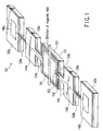
- FIG. 1 is a perspective view of essential parts of a light deflector in a first embodiment of the present invention.
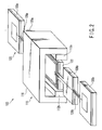
- FIG. 2 is a perspective view of the entire light deflector in the first embodiment of the present invention.
- FIG. 3 is a plan view of the light deflector shown in FIG. 2.
- a light deflector 100 in the present embodiment has a first movable plate 122, a pair of second movable plates 126a and 126b located on both sides of the first movable plate 122, a pair of first hinges (torsion bar hinges) 124a and 124b connecting the second movable plates 126a and 126b to the first movable plate 122, a pair of fixing portions 130a and 130b located outside the second movable plates 126a and 126b, and a pair of second hinges 128a and 128b connecting the second movable plates 126a and 126b to the fixing portions 130a and 130b, respectively.
- first hinges tilt bar hinges
- the fixing portions 130a and 130b are configured with separate members in the present embodiment, but are not limited thereto, and may be formed with one member. That is, the fixing portions 130a and 130b may be, for example, part of a member having a frame shape such as a U-shape or square shape that extends around the first movable plate 122 and the second movable plates 126a and 126b.
- the first movable plate 122 has a reflective surface 132 on one of main surfaces.
- the main surfaces of the first movable plate 122 represent the two largest parallel planes, that is, an upper surface and a lower surface in FIG. 1.
- the upper surface and the lower surface represent the upper visible surface and the invisible hidden surface on a rear side, respectively, in FIG. 1.
- the first movable plate 122 has the reflective surface 132 on its lower surface.
- the first hinges 124a and 124b and the second hinges 128a and 128b are both made of a torsionally deformable elastic material, so that the first movable plate 122 can oscillate with respect to the second movable plates 126a and 126b, and the second movable plates 126a and 126b can oscillate with respect to the fixing portions 130a and 130b.
- oscillating basically refers to repetitive reciprocating vibration about a predetermined virtual axis, but also includes simple inclination about the predetermined virtual axis.
- oscillating of the movable plate means that the movable plate inclines or repetitively vibrates about an axis.
- the predetermined virtual axis in the oscillating operation will hereinafter be called an oscillation axis.
- the oscillation axis of the first hinges 124a and 124b and the oscillation axis of the second hinges 128a and 128b are located on the same axis, and the stiffness of the second hinges 128a and 128b against oscillation is lower than the stiffness of the first hinges 124a and 124b against oscillation.
- a structure comprising the first movable plate 122, the first hinges 124a and 124b, the second movable plates 126a and 126b, the second hinges 128a and 128b and the fixing portions 130a and 130b will hereinafter be called a movable plate unit 120.
- the movable plate unit 120 has the first movable plate 122 with the reflective surface 132, the pair of fixing portions 130a and 130b located on both sides of the first movable plate 122, the pair of second movable plates 126a and 126b located between the first movable plate 122 and the fixing portions 130a and 130b, the pair of first hinges 124a and 124b supporting the first movable plate 122 so as to allow it to oscillate with respect to the second movable plates 126a and 126b, and the pair of second hinges 128a and 128b supporting the second movable plates 126a and 126b so as to allow them to oscillate with respect to the fixing portions 130a and 130b.
- the movable plate unit 120 further has a drive coil 142 provided in the first movable plate 122, and extraction electrodes 146a and 146b provided on the fixing portions 130a and 130b, respectively.
- the drive coil 142 goes around near the edge of the first movable plate 122.
- An outer end of the drive coil 142 is electrically connected to the extraction electrode 146a on the fixing portion 130a via a wire 144a passing the first hinge 124a, the second movable plate 126a and the second hinge 128a.
- an inner end of the drive coil 142 is connected to a contact pad 152, and the contact pad 152 is electrically connected to a contact pad 156 provided outside the drive coil 142 via a bridge wire 154, which crosses over the drive coil 142 through an insulating layer.
- the contact pad 156 is electrically connected to the extraction electrode 146b on the fixing portion 130b via a wire 144b passing the first hinge 124b, the second movable plate 126b and the second hinge 128b.
- These electric elements are provided on the upper side of the movable plate unit 120, and are covered with an insulating film, which is not shown in the drawing, except for the extraction electrodes 146a and 146b.
- the light deflector 100 further has a pair of permanent magnets 112a and 112b located on both sides of the first movable plate 122, and a yoke 116 made of a magnetic material supporting the permanent magnets 112a and 112b.
- the permanent magnets 112a and 112b constitute a magnetic field generator to generate a magnetic field crossing the first movable plate 122.
- a structure comprising the permanent magnets 112a and 112b and the yoke 116 constitute a magnetic circuit 110.
- the permanent magnets 112a and 112b are magnetized in parallel with the main surfaces (the upper surface and the lower surface) of the first movable plate 122 in an un-oscillating state, and produce a magnetic field directed from one side to the other, for example, a magnetic field directed from the permanent magnet 112a to the permanent magnet 112b.
- the magnetic field produced by the permanent magnets 112a and 112b is substantially vertical to the oscillation axis, and is substantially parallel to the surfaces of the first movable plate 122 in the un-oscillating state.
- the drive coil 142 on the first movable plate 122 and the permanent magnets 112a and 112b located on both sides of the first movable plate 122 constitute actuating means or an actuator to oscillate the first movable plate 122.
- FIG. 4A to FIG. 4H show processes of manufacturing the movable plate unit 120.
- FIG. 5 shows the position of the section shown in FIG. 4A to FIG. 4H. That is, the section shown in FIG. 4A to FIG. 4H is the section of the movable plate unit 120 along the section IV - IV section of FIG. 5.
- the movable plate unit 120 is manufactured by MEMS manufacturing technology using a SOI wafer.
- FIG. 4A shows a SOI wafer 600.
- the SOI wafer 600 is a substrate in which two layers of silicon substrates 602 and 606 are affixed via a bonding layer 604 which is an insulating layer.
- the two layers of silicon substrates 602 and 606 both comprise substrates having a specific resistance of about 5 ⁇ cm used for ordinary semiconductor manufacture.
- the bonding layer 604, which has a thickness of about 1 ⁇ m, comprises a silicon oxide film.
- the silicon substrate 606 located on the upper side of the drawing is called a device layer
- the silicon substrate 602 located on the lower side is called a handle layer.
- a silicon oxide film 608 is formed on the device layer 606.
- the silicon oxide film 608 is an insulating material, and insulates the electric elements including the drive coil 142, the wires 144a and 144b and the extraction electrodes 146a and 146b, which will be formed later, from the device layer 606.
- a conductive film 610 is formed on the silicon oxide film 608 and patterned to form the drive coil 142, the wires 144a and 144b and the extraction electrodes 146a and 146b.
- the conductive film 610 comprises, for example, an aluminum film formed by a sputter.
- a passivation film 612 is formed on the conductive film 610 for insulation from the air and patterned such that the passivation film 612 is formed on the drive coil 142 and the wires 144a and 144b.
- the patterning parts of the passivation film corresponding to the extraction electrodes 146a and 146b on the fixing portion 130a and 130b, and to the contact pads 152 and 156 for the bridge wire 154 are removed.
- a conductive film 614 is formed on the passivation film 612 and patterned to form the bridge wire 154. Further, the bridge wire 154 is covered with an insulating film 616.
- the conductive film 614 is, for example, an aluminum film formed by the sputter film forming device, but may be a film of a material different from those of the wires and the like.
- the device layer 606 is vertically passed through by a dry etching device, and a layer of the first movable plate 122, the second movable plates 126a and 126b and the fixing portions 130a and 130b, the first hinges 124a and 124b, and the second hinges 128a and 128b are formed.
- the handle layer 602 is vertically passed through by the dry etching device, and the first movable plate 122, the second movable plates 126a and 126b and the fixing portions 130a and 130b are formed.
- the reflective surface 132 is formed on the surface at the handle layer 602, that is, the lower surface of the first movable plate 122, thus attaining completion.
- the reflective surface depends on the wavelength of light to be deflected, and includes, for example, surface of an aluminum film, a gold film, a dielectric multilayer film or the like.
- FIG. 6 is a diagram to explain the principle of actuating the light deflector 100.
- the external power supply 158 is a direct-current power supply and the current passing through the drive coil 142 is a direct current
- the couple acting on and the first movable plate 122 is constant, so that the first movable plate 122 is inclined about the oscillation axis.
- the angle of inclination of the first movable plate 122 depends on the intensity of the current passing through the drive coil 142.
- the couple acting on the first movable plate 122 changes direction and magnitude periodically, so that the first movable plate 122 oscillates about the oscillation axis.
- the oscillation angle of the first movable plate 122 depends on the extent of amplitude of the alternating current passing through the drive coil 142.
- FIG. 7 is a graph wherein an alternating current is passed through the drive coil 142 of the light deflector 100, and the frequency of the alternating current is changed to cause changes in the oscillation angle of the first movable plate 122.
- FIG. 7 shows oscillation angle characteristics of the first movable plate 122 with regard to the frequencies of the alternating current flowing through the drive coil 142.
- the horizontal axis indicates the frequency of alternating current flowing through the drive coil 142
- the vertical axis indicates the normalized oscillation angle of the first movable plate 122.
- peaks in the vicinity of 700 Hz and 5 kHz indicate a resonant state about the oscillation axis of the first movable plate 122.
- a low-frequency resonance in the vicinity of 700 Hz is called a first resonance
- a high-frequency resonance in the vicinity of 5 kHz is called a second resonance. That is, the light deflector 100 has two resonance frequencies, and a lower first resonance frequency is at a value close to 700 Hz and a higher second resonance frequency is at a value close to 5 kHz.
- the first movable plate 122 and the second movable plates 126a and 126b oscillate in phase in a frequency region ranging from 0 to the vicinity of the first resonance frequency, as shown in FIG. 8. Further, the first movable plate 122 and the second movable plates 126a and 126b oscillate in opposite phase in a frequency region around the second resonance frequency, as shown in FIG. 9.
- the light deflector 100 is designed so that the required oscillation angle (actuating efficiency) is obtained at a frequency lower than the first resonance frequency. As shown in FIG. 7, in the second resonance, actuating efficiency higher than the actuating efficiency that is obtained at a frequency lower than the first resonance frequency is obtained.
- the second resonance is used in high-speed scanning for screening to decide an observing position. It is necessary to change the scanning rate depending on characteristics of a fluorescent material and observation conditions in low-speed scanning to obtain an image.
- a low-speed scanning region should desirably be set at a frequency lower than the first resonance frequency. If the light deflector 100 is to be used at or beyond the first resonance frequency, the oscillation angle extremely increases in the vicinity of the first resonance frequency, so that a system that detects and controls the oscillation angle is required. If a premise is made that the system of controlling the oscillation angle is provided, the light deflector 100 may be used beyond the first resonance frequency. However, as the actuating efficiency to be obtained is reduced due to an increase in the frequency, there is a limit in the range of frequencies that can be used.
- the actuating efficiency of the first movable plate 122 in the low-speed scanning region depends on a driving force depending on a spatial magnetic flux density obtained by the permanent magnets 112a and 112b and the amount of current flowing through the drive coil 142, and the torsional stiffness of the second hinges 128a and 128b.
- the actuating efficiency of the first movable plate 122 in the high-speed scanning region actuated in a second resonant state is influenced by the moment of inertia of the first movable plate 122 and the moment of inertia of the second movable plates 126a and 126b, in addition to the driving force and the torsional stiffness of the first hinges 124a and 124b.
- the second movable plates 126a and 126b oscillate in opposite phase with the first movable plate 122.
- the moment of inertia has an effect especially on the ratio between the actuating efficiency of the first movable plate 122 and the actuating efficiency of the second movable plates 126a and 126b.
- the first movable plate 122 desirably has an actuating efficiency higher than that of the second movable plates 126a and 126b. If the total moment of inertia of the two second movable plates 126a and 126b provided on both sides of the first movable plate 122 is made larger than the moment of inertia of the first movable plate 122, the actuating efficiency of the first movable plate 122 becomes larger than the actuating efficiency of the second movable plates 126a and 126b, resulting in an improvement of the actuating efficiency.
- the actuating efficiency of the first movable plate 122 and the second movable plates 126a and 126b changes in accordance with the difference between their moment of inertia. If the total moment of inertia of the second movable plates 126a and 126b is smaller than the moment of inertia of the first movable plate 122, the second movable plates 126a and 126b oscillate more largely, and in a contrary case, the first movable plate 122 oscillates more largely. If the total moment of inertia of the second movable plates 126a and 126b further increases, the second movable plates 126a and 126b hardly oscillate and the first movable plate 122 alone will oscillate. It is to be noted that the total moment of inertia of the second movable plates 126a and 126b is preferably set to such a degree that a desired the low-speed scanning region is ensured.
- the low-speed scanning region ranges from DC (frequency 0) to less than the first resonance, and the first resonance frequency decides the low-speed scanning region.
- Fr is the resonance frequency
- k is the polar moment of inertia of area of the second hinges 128a and 128b
- G is a modulus of transverse elasticity of the second hinges 128a and 128b
- L is the length of the second hinges 128a and 128b
- 1 is the total moment of inertia of the first movable plate 122 and the second movable plates 126a and 126b including the first hinges 124a and 124b.
- the first movable plate 122 and the second movable plates 126a and 126b have the same thickness, and it is difficult to make a difference in their thickness considering the manufacturing method. Therefore, sizes other than the thickness need to be changed to increase the moment of inertia, but to increase the number of movable plate units 120, the width (dimension along an axis vertical to the oscillation axis) of the second movable plates 126a and 126b should be adapted to the width of the first movable plate 122. Therefore, the moment of inertia of the second movable plates 126a and 126b may desirably be adjusted by changing the length (dimension along the oscillation axis) of the second movable plates.
- the light deflector 100 in the present embodiment has the actuating efficiency sufficient to be able to support both the low-speed scanning in which an actuating frequency is variable and the high-speed scanning in which the actuating frequency is fixed. Further, the total moment of inertia of the second movable plates 126a and 126b can be optimized to expand the low-speed scanning region, so that the actuating frequency can be changed in a wide range.
- the configuration in the present embodiment can naturally be variously changed and modified.
- FIG. 10 is a perspective view of the movable plate unit according to the first modification
- FIG. 11 is a top view of the movable plate unit shown in FIG. 10.
- members indicated by the same reference numerals as the members shown in FIG. 1 are the same and will not be described in detail.
- the difference between a movable plate unit 220 in the present modification and the movable plate unit 120 in FIG. 1 lies in the form of second movable plates 226a and 226b.
- the second movable plates 226a and 226b are provided with notches at portions located on both sides of the first hinges 124a and 124b and the second hinges 128a and 128b. In this way, the length of the movable plate unit 220 is reduced as compared with that of the movable plate unit 120 in the first embodiment while the first hinges 124a and 124b and the second hinges 128a and 128b maintain the same length as in the first embodiment.
- FIG. 12 is a top view of the light deflector according to the second modification.
- members indicated by the same reference numerals as the members shown in FIG. 1 are the same and will not be described in detail.
- a movable plate unit 320 has, in addition to the configuration of the movable plate unit 120 of the first embodiment, second drive coils 342a and 342b provided in the second movable plates 126a and 126b, respectively, and two pairs of extraction electrodes 346a and 346b provided in the fixing portions 130a and 130b, respectively.
- the second drive coils 342a and 342b go around near the edges of the second movable plates 126a and 126b, respectively.
- Outer ends of the second drive coils 342a and 342b are electrically connected to the extraction electrodes 346a and 346a, respectively, which are provided in the fixing portions 130a and 130b, respectively, via wires 344a and 344a passing the second hinges 128a and 128b.
- outer ends of the second drive coils 342a and 342b are connected to contact pads 352a and 352b, respectively, and the contact pads 352a and 352b are electrically connected to contact pads 356a and 356b, respectively, which are provided outside the second drive coils 342a and 342b, via bridge wires 354a and 354b which cross over the second drive coils 342a and 342b through insulating layers.
- the contact pads 356a and 356b are electrically connected to the extraction electrodes 346b and 346b, respectively, which are provided in the fixing portions 130a and 130b, respectively, via wires 344b and 344b passing the second hinges 128a and 128b.
- These electric elements are provided on the upper side of the movable plate unit 320, and are covered with an insulating film, which is not shown in the drawing, except for the extraction electrodes 346a and 346b.
- a pair of permanent magnets 312a and 312b and a yoke 316 constituting a magnetic circuit 310 have a length to be located on both sides of the first movable plate 122 and the second movable plates 126a and 126b. That is, the dimension of the permanent magnets 312a and 312b and the yoke 316 along the oscillation axis is larger than the total length of the first movable plate 122, the first hinges 124a and 124b and the second movable plates 126a and 126b.
- the permanent magnets 312a and 312b constitute a magnetic field generator to generate a magnetic field crossing the first movable plate 122 and the second movable plates 126a and 126b.
- the second drive coils 342a and 342b provided in the second movable plates 126a and 126b, respectively, and the permanent magnets 312a and 312b located on both sides of the second movable plates 126a and 126b constitute actuating means or an actuator to oscillate the second movable plates 126a and 126b.
- the actuating means or actuator the second movable plates 126a and 126b oscillate in totally the same manner as in the principle of oscillating the first movable plate 122.
- the actuating means or actuator to oscillate the second movable plates 126a and 126b can be used to improve the actuating efficiency of oscillating the first movable plate 122.
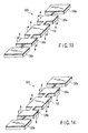
- a current may preferably be passed through the second drive coils 342a and 342b in the same direction as the drive coil 142, as shown in FIG. 13.
- a couple in the same direction as the couple acting on the first movable plate 122 works on the second movable plates 126a and 126b, so that the force to oscillate the first movable plate 122 is practically improved. This results in an improvement in the actuating efficiency of the first movable plate 122.
- a current may also be preferably passed through the second drive coils 342a and 342b in the same direction as the drive coil 142, as shown in FIG. 14.
- the couple in the same direction as the couple acting on the first movable plate 122 works on the second movable plates 126a and 126b, so that the oscillation of the second movable plates 126a and 126b is restricted. This is equivalent to an increase in the apparent moment of inertia of the second movable plates 126a and 126b. Therefore, the force to oscillate the first movable plate 122 is practically improved.
- a third modification is directed to a light deflector having actuating means or an actuator different from that in the first embodiment to oscillate the first movable plate 122.
- FIG. 15 is a perspective view of the light deflector according to the third modification.
- members indicated by the same reference numerals as the members shown in FIG. 1 are the same and will not be described in detail.
- the actuating means or actuator in the third modification comprises an electrode provided in the first movable plate 122, and electrodes provided to face the electrode in the first movable plate 122.
- a light deflector 400 according to the third modification has an electrode plate 442 provided in the first movable plate 122, and two drive electrode plates 452a and 452b disposed with a space to face the electrode plate 442.
- the two drive electrode plates 452a and 452b are disposed with a space in parallel with the oscillation axis. Further, in a projection of the two drive electrode plates 452a and 452b to the first movable plate 122, the two drive electrode plates 452a and 452b are located with the oscillation axis in between.
- the electrode plate 442 on the first movable plate 122 is electrically connected to extraction electrodes 446a and 446b that are provided in the fixing portions 130a and 130b, respectively, via wires 444a and 444a passing the first hinges 124a and 124b, the second movable plates 126a and 126b and the second hinges 128a and 128b.
- the electrode plate 442 on the first movable plate 122 is maintained at a constant potential, for example, a GND potential. Moreover, the two drive electrode plates 452a and 452b facing the electrode plate 442 are provided with different potentials by external power supplies 458a and 458b, respectively. Thus, different intensities of electrostatic attractions are produced between one of the drive electrode plates 452a and 452b and the electrode plate 442 on the first movable plate 122 and between the other one of the drive electrode plates 452a and 452b and the electrode plate 442 on the first movable plate 122. Therefore, the first movable plate 122 is subjected to a torque about the oscillation axis.
- the first movable plate 122 is subjected to a counterclockwise torque (a torque in a rotating direction to bring the electrode plate 442 close to the drive electrode plate 452a) if Va > Vb, and the first movable plate 122 is, on the contrary, subjected to a clockwise torque (a torque in a rotating direction to bring the electrode plate 442 close to the drive electrode plate 452b) if Va ⁇ Vb.
- the external power supplies 458a and 458b are direct-current power supplies and the voltage applied across the electrode plate 442 and the drive electrode plates 452a and 452b is constant, the force acting on the first movable plate 122 is constant, so that the first movable plate 122 is inclined about the oscillation axis. In that case, the angle of inclination of the first movable plate 122 depends on the intensity of the constant voltage applied across the electrode plate 442 and the drive electrode plates 452a and 452b.
- the force acting on the first movable plate 122 changes direction and magnitude periodically, so that the first movable plate 122 oscillates about the oscillation axis.
- the oscillation angle of the first movable plate 122 depends on the extent of amplitude of the alternating voltage applied across the electrode plate 442 and the drive electrode plates 452a and 452b.
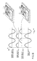
- the alternating voltages Va and Vb applied across the electrode plate 442 and the drive electrode plates 452a and 452b, respectively, preferably have substantially sinusoidal waveforms in opposite phase with each other to which a constant offset voltage is applied, as shown in FIG. 16.
- the first movable plate 122 is actuated along the sinusoidal waveform of the drive voltage, and is actuated such that the phase is lagged by 90 degrees with respect to the drive voltage in a resonant state.
- An actuating method of the present embodiment has an advantage that the actuating efficiency is lower than that in an actuating method using the drive coil and that the oscillation angle to be obtained is small, but the configuration is simple. It is therefore useful for applications wherein a high actuating efficiency or a large oscillation angle is not needed.
- the similar actuating means or actuator can also be provided for the second movable plates, as in the second modification. In that case, the similar effects as in the second modification can also be expected.
- a fourth modification is directed to an improvement of the light deflector of the first embodiment.
- the light deflector of the present modification has a configuration in which a capacitive sensing type oscillation angle detection function to detect the oscillation angle of the second movable plates is added to the light deflector of the first embodiment.
- the principle of actuating the first movable plate 122 is the same as that in the first embodiment.
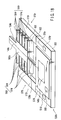
- FIG. 17 is a perspective view of the movable plate unit in the light deflector according to the fourth modification.
- members indicated by the same reference numerals as the members shown in FIG. 1 are the same and will not be described in detail.
- second movable plates 560a and 560b that are located between the first hinges 124a and 124b and the second hinges 128a and 128b, respectively, have comb teeth 562r and 562l extending outward on both sides substantially vertically to the oscillation axis.
- each of fixing portions 530a and 530b has a pair of extensions 570r and 570l located on both sides of the second movable plates 560a and 560b.
- the extensions 570r and 570l have comb teeth 572r and 572l extending inward on both sides substantially vertically to the oscillation axis, respectively.
- the comb teeth 562r and 562l of the second movable plates 560a and 560b and the comb teeth 572r and 572l of the extensions 570r and 570l break into each other's spaces between the teeth.
- FIG. 18 shows, in an enlarged manner, the second movable plate, the second hinge and the fixing portion on a near side of FIG. 17. Therefore, FIG. 18 only shows the configuration of the second movable plate, the second hinge and the fixing portion on the near side of FIG. 17, but the second movable plate, the second hinge and the fixing portion on the far side of FIG. 17 naturally have the same configuration.
- reference numerals of the second movable plate, the second hinge and the fixing portion on the far side of FIG. 17 will be noted together.
- the second movable plates 560a and 560b include the device layer 606 and the handle layer 602. Further, parts of the device layer 606 located at the second movable plates 560a and 560b, the second hinges 128a and 128b and the fixing portions 530a and 530b have been doped by, for example, an ion implantation technique, so that electric resistance of surface parts are reduced.
- the comb teeth 562r and 562l of the second movable plates 560a and 560b serve as electrodes only in the part corresponding to the device layer 606.
- the part of the comb teeth 562r and 562l of the second movable plates 560a and 560b corresponding to the device layer 606 will hereinafter be called movable side comb teeth electrodes 564r and 564l.
- the extensions 570r and 570l is made from the handle layer 602, and an insulating film such as a silicon oxide film, which is not shown, is provided on the handle layer 602.
- an insulating film such as a silicon oxide film, which is not shown, is provided on the handle layer 602.
- a conductive thin film made of aluminum or the like is formed and patterned to provide electrode portions 573r and 573l located on upper surfaces of the extensions 570r and 570l, fixed side extraction electrodes 578r and 578l located in the fixing portions 530a and 530b, and wires 576r and 576l electrically connecting the electrode portions 573r and 573l and the fixed side extraction electrodes 578r and 578l.
- Parts of the electrode portions 573r and 573l located on the comb teeth 572r and 572l of the extensions 570r and 570l will hereinafter be called fixed side comb teeth electrodes 574r and 574l.
- the movable side comb teeth electrode 564r and the fixed side comb teeth electrode 574r on the right side constitute a right side capacitive sensor 580r
- the movable side comb teeth electrode 564l and the fixed side comb teeth electrode 574l on the left side constitute a left side capacitive sensor 580l.
- the electrode portion 573r, the wire 576r and the fixed side extraction electrode 578r on the right side are electrically independent from the electrode portion 573l, the wire 576l and the fixed side extraction electrode 578l on the left side, the capacitance between the movable side comb teeth electrode 564r and the fixed side comb teeth electrode 574r on the right side and the capacitance between the movable side comb teeth electrode 564l and the fixed side comb teeth electrode 574l on the left side are detected independently.
- the right side capacitive sensor 580r and the left side capacitive sensor 580l i.e., the movable side comb teeth electrodes 564r and 564l and the fixed side comb teeth electrodes 574r and 574l cooperate with an oscillation angle detection circuit described later to constitute detecting means or a detector to detect the oscillation angle of the second movable plates 560a and 560b.
- FIG. 19 shows a configuration of the oscillation angle detection circuit which detects the oscillation angle of the second movable plates 560a and 560b.
- the oscillation angle detection circuit has a first detection circuit 592r to detect the clockwise oscillation angle of the second movable plates 560a and 560b, a second detection circuit 592l to detect the counterclockwise oscillation angle of the second movable plates 560a and 560b, and a subtractor 598 for subtraction processing of an output of the first detection circuit 592r and an output of the second detection circuit 592l.
- the first detection circuit 592r has a capacitive-amplitude conversion circuit 594r and an amplitude detection circuit 596r
- the second detection circuit 592l similarly has a capacitive-amplitude conversion circuit 594l and an amplitude detection circuit 596l.
- the capacitance-amplitude conversion circuit 594r applies a voltage signal having a frequency far beyond the actuating frequency across the movable side extraction electrode 568 and the fixed side extraction electrode 578r.
- the capacitance-amplitude conversion circuit 594l applies a voltage signal, which is the same as that applied by the capacitance-amplitude conversion circuit 594r, across the movable side extraction electrode 568 and the fixed side extraction electrode 578l.
- the movable side extraction electrode 568 is maintained at a GND potential, and the capacitance-amplitude conversion circuits 594r and 594l apply the above-mentioned voltage signals to the fixed side extraction electrodes 578r and 578l.
- the movable side comb teeth electrodes 564r and 564l are both formed on the device layer 606, and the fixed side comb teeth electrodes 574r and 574l are both formed on the handle layer 602.
- the area of a part where the movable side comb teeth electrodes 564r and 564l face the fixed side comb teeth electrodes 574r and 574l is 0.
- the movable side comb teeth electrodes 564r and 564l and the fixed side comb teeth electrodes 574r and 574l do not at all overlap each other.
- the capacities between the movable side comb teeth electrodes 564r and 564l and between the fixed side comb teeth electrodes 574r and 574l are both 0.
- the area of the part where the movable side comb teeth electrode 564r and the fixed side comb teeth electrode 574r will be the maximum, and the capacitance between the movable side comb teeth electrode 564r faces the fixed side comb teeth electrode 574r will be the maximum.
- the movable side comb teeth electrode 564l and the fixed side comb teeth electrode 574l are farther away from each other than when the oscillation angle of the second movable plates 560a and 560b is 0, so that the capacitance between them is still 0.
- C is the capacitance
- ⁇ 0 is a relative dielectric constant
- S is the area of the facing electrodes
- d is the space between the electrodes.
- the capacitance-amplitude conversion circuit 594r detects the voltage across the movable side extraction electrode 568 and the fixed side extraction electrode 578r.
- the capacitance-amplitude conversion circuit 594l detects the voltage across the movable side extraction electrode 568 and the fixed side extraction electrode 578l. Detection signals of the capacitance-amplitude conversion circuits 594r and 594l will be the above-mentioned high-frequency voltage signals on which the capacitance changes between the movable side comb teeth electrodes 564r and 564l and between the fixed side comb teeth electrodes 574r and 574l are superposed.
- the amplitude detection circuits 596r and 5961 only extract signal components corresponding to the capacitance changes between the movable side comb teeth electrodes 564r and 564l and between the fixed side comb teeth electrodes 574r and 574l from the detection signals of the capacitance-amplitude conversion circuits 594r and 594l.
- the output of the amplitude detection circuit 596r and the output of the amplitude detection circuit 596l are subjected to the subtraction processing by the subtractor 598 and will be final detection signals.
- FIG. 20 shows output signals of the first detection circuit 592r, the second detection circuit 592l and the subtractor 598 with regard to the oscillation angle of the second movable plates 560a and 560b.
- the horizontal axis represents time and the vertical axis represents the oscillation angle and gains of the respective signals.
- the oscillation angle is positive in a clockwise direction and negative in a counterclockwise direction.
- the output signal emerges in one of the first detection circuit 592r and the second detection circuit 592l depending on the oscillation direction of the second movable plates 560a and 560b, that is, depending on whether the oscillation angle is positive or negative, but the output signal does not emerge in the other one. More specifically, when the second movable plates 560a and 560b oscillate in a clockwise direction, that is, when the oscillation angle is positive, the output signal emerges in the first detection circuit 592r while the output signal does not emerge in the second detection circuit 592l.
- the output signal of the subtractor 598 is produced by subtracting the output signal of the second detection circuit 592l from the output signal of the first detection circuit 592r, and changes in phase with the oscillation angle of the second movable plates 560a and 560b. Therefore, it is possible to know the oscillation angle and oscillation direction of the second movable plates 560a and 560b from the output signal of the subtractor 598.
- the second movable plates 560a and 560b oscillate in phase with the first movable plate 122. It is therefore possible to know the oscillation angle of the first movable plate 122 on the basis of the output signal of the subtractor 598.
- a resonant actuation is performed such that the second movable plates 560a and 560b oscillate in opposite phase with the first movable plate 122.
- the oscillation angle of the first movable plate 122 and the oscillation angle of the second movable plates 560a and 560b differ depending on their moment of inertia. It is therefore difficult to predict the oscillation angle of the first movable plate 122 from the oscillation angle of the second movable plates 560a and 560b.
- the drive coil 142 may preferably be used to detect the oscillation angle of the first movable plate 122 in accordance with a technique disclosed in US 2003/042801. More specifically, time to supply a drive current to the drive coil 142 and time to detect induced electromotive force produced in the drive coil 142 are set such that the supply of drive current and the detection of the induced electromotive force are alternately repeated. A speed signal of the first movable plate 122 is obtained by the detection of the induced electromotive force, and the signal is integrated to acquire information on the oscillation angle of the first movable plate 122.
- a light deflector 500 in the present modification has the detection function to detect the oscillation angle of the second movable plates 560a and 560b, so that it is possible to know the oscillation angle and oscillation direction of the first movable plate 122 in low-speed scanning state.
Landscapes
- Physics & Mathematics (AREA)
- General Physics & Mathematics (AREA)
- Optics & Photonics (AREA)
- Mechanical Optical Scanning Systems (AREA)
- Micromachines (AREA)
Applications Claiming Priority (2)
| Application Number | Priority Date | Filing Date | Title |
|---|---|---|---|
| JP2003370900 | 2003-10-30 | ||
| JP2003370900A JP4262574B2 (ja) | 2003-10-30 | 2003-10-30 | 光偏向器 |
Publications (1)
| Publication Number | Publication Date |
|---|---|
| EP1528422A1 true EP1528422A1 (de) | 2005-05-04 |
Family
ID=34420209
Family Applications (1)
| Application Number | Title | Priority Date | Filing Date |
|---|---|---|---|
| EP04025807A Withdrawn EP1528422A1 (de) | 2003-10-30 | 2004-10-29 | Lichtablenker |
Country Status (3)
| Country | Link |
|---|---|
| US (1) | US7123400B2 (de) |
| EP (1) | EP1528422A1 (de) |
| JP (1) | JP4262574B2 (de) |
Cited By (5)
| Publication number | Priority date | Publication date | Assignee | Title |
|---|---|---|---|---|
| WO2008054424A3 (en) * | 2005-10-31 | 2008-07-31 | Advanced Numicro Systems Inc | Mems mirror with parallel springs and arched support for beams |
| WO2008153221A1 (en) * | 2007-06-14 | 2008-12-18 | Canon Kabushiki Kaisha | Oscillator device, optical deflecting device and method of controlling the same |
| US7821693B1 (en) | 2006-12-06 | 2010-10-26 | Advanced Numicro Systems, Inc. | MEMS mirror with rotation amplification and electromagnetic drive |
| EP1949168A4 (de) * | 2005-09-16 | 2011-09-14 | Texas Instruments Inc | Magnet-auf-rahmen-oszillationseinrichtung |
| CN109725414A (zh) * | 2017-10-30 | 2019-05-07 | 英飞凌科技股份有限公司 | 具备具有开口的板簧的镜子器件 |
Families Citing this family (16)
| Publication number | Priority date | Publication date | Assignee | Title |
|---|---|---|---|---|
| JP4385938B2 (ja) * | 2004-12-15 | 2009-12-16 | セイコーエプソン株式会社 | アクチュエータ |
| JP4694196B2 (ja) * | 2004-12-28 | 2011-06-08 | オリンパス株式会社 | 光偏向器 |
| JP5170983B2 (ja) | 2006-05-30 | 2013-03-27 | キヤノン株式会社 | 光偏向器、及びそれを用いた光学機器 |
| KR100773535B1 (ko) * | 2006-06-14 | 2007-11-05 | 삼성전기주식회사 | 맴스 디바이스 |
| JP4946568B2 (ja) * | 2007-03-28 | 2012-06-06 | 株式会社デンソー | 光走査装置 |
| CA2764403C (en) * | 2007-04-19 | 2014-02-11 | Nippon Telegraph And Telephone Corporation | Micromirror element and micromirror array |
| DE102008042967B4 (de) * | 2008-10-20 | 2017-04-06 | Robert Bosch Gmbh | Kaskadierte mikromechanische Aktuatorstruktur |
| JP5157835B2 (ja) * | 2008-11-12 | 2013-03-06 | セイコーエプソン株式会社 | 画像表示装置 |
| US20100141366A1 (en) * | 2008-12-04 | 2010-06-10 | Microvision, Inc. | Magnetically Actuated System |
| JP5205352B2 (ja) * | 2009-09-11 | 2013-06-05 | アオイ電子株式会社 | 昇圧回路 |
| DE102010029539B4 (de) * | 2010-06-01 | 2018-03-08 | Robert Bosch Gmbh | Mikromechanisches Bauteil und Herstellungsverfahren für ein mikromechanisches Bauteil |
| DE102013206396A1 (de) * | 2013-04-11 | 2014-10-16 | Fraunhofer-Gesellschaft zur Förderung der angewandten Forschung e.V. (FHG) | Mikroaktuatoranordnung zur Ablenkung elektromagnetischer Strahlung |
| WO2015092938A1 (ja) * | 2013-12-20 | 2015-06-25 | パイオニア株式会社 | 駆動装置 |
| CN104748669A (zh) * | 2013-12-30 | 2015-07-01 | 光宝科技股份有限公司 | 静电式微扫描镜的角度检测电路 |
| WO2020122278A1 (ko) * | 2018-12-12 | 2020-06-18 | 엘지전자 주식회사 | 멤스 스캐너 |
| US12140751B2 (en) * | 2020-01-09 | 2024-11-12 | Texas Instruments Incorporated | Fringing-field, parallel plate actuator |
Citations (4)
| Publication number | Priority date | Publication date | Assignee | Title |
|---|---|---|---|---|
| EP0620415A1 (de) * | 1993-04-16 | 1994-10-19 | Murata Manufacturing Co., Ltd. | Winkelgeschwindigkeitsmessaufnehmer |
| US5543956A (en) * | 1992-10-08 | 1996-08-06 | Fuji Electric Co., Ltd. | Torsional vibrators and light deflectors using the torsional vibrator |
| US20020118429A1 (en) * | 2000-12-18 | 2002-08-29 | Olympus Optical Co., Ltd. | Mirror rocking member for optical deflector |
| WO2002099504A2 (de) * | 2001-04-12 | 2002-12-12 | Jenoptik Ldt Gmbh | Resonanzscanner |
Family Cites Families (11)
| Publication number | Priority date | Publication date | Assignee | Title |
|---|---|---|---|---|
| JP2579111B2 (ja) * | 1992-12-15 | 1997-02-05 | 松下電器産業株式会社 | 静電力駆動小型光スキャナ |
| JP2849697B2 (ja) * | 1993-03-12 | 1999-01-20 | 工業技術院長 | 2自由度振動型マイクロアクチュエータ |
| JPH0792409A (ja) * | 1993-09-27 | 1995-04-07 | Canon Inc | 光スキャナー |
| US5808707A (en) * | 1995-03-01 | 1998-09-15 | Canon Kabushiki Kaisha | Display apparatus |
| JP2000162538A (ja) * | 1998-11-30 | 2000-06-16 | Mitsubishi Electric Corp | マイクロミラー装置 |
| JP2001091889A (ja) * | 1999-09-24 | 2001-04-06 | Victor Co Of Japan Ltd | 光偏向器及びこれを用いた表示装置 |
| US6865064B2 (en) | 2001-08-29 | 2005-03-08 | Olympus Corporation | Drive apparatus and drive method for electromagnetic drive actuator |
| US7248390B2 (en) * | 2002-03-26 | 2007-07-24 | Pentax Corporation | Light scanning device |
| JP4147947B2 (ja) * | 2003-01-21 | 2008-09-10 | 日産自動車株式会社 | 光走査装置及びこれを用いた物体検出装置、描画装置 |
| US8054522B2 (en) * | 2003-04-21 | 2011-11-08 | Technion Research & Development Foundation Ltd. | Oscillating mirror having a plurality of eigenmodes |
| JP4492252B2 (ja) * | 2003-09-05 | 2010-06-30 | セイコーエプソン株式会社 | アクチュエータ |
-
2003
- 2003-10-30 JP JP2003370900A patent/JP4262574B2/ja not_active Expired - Fee Related
-
2004
- 2004-10-28 US US10/975,882 patent/US7123400B2/en not_active Expired - Fee Related
- 2004-10-29 EP EP04025807A patent/EP1528422A1/de not_active Withdrawn
Patent Citations (4)
| Publication number | Priority date | Publication date | Assignee | Title |
|---|---|---|---|---|
| US5543956A (en) * | 1992-10-08 | 1996-08-06 | Fuji Electric Co., Ltd. | Torsional vibrators and light deflectors using the torsional vibrator |
| EP0620415A1 (de) * | 1993-04-16 | 1994-10-19 | Murata Manufacturing Co., Ltd. | Winkelgeschwindigkeitsmessaufnehmer |
| US20020118429A1 (en) * | 2000-12-18 | 2002-08-29 | Olympus Optical Co., Ltd. | Mirror rocking member for optical deflector |
| WO2002099504A2 (de) * | 2001-04-12 | 2002-12-12 | Jenoptik Ldt Gmbh | Resonanzscanner |
Cited By (9)
| Publication number | Priority date | Publication date | Assignee | Title |
|---|---|---|---|---|
| EP1949168A4 (de) * | 2005-09-16 | 2011-09-14 | Texas Instruments Inc | Magnet-auf-rahmen-oszillationseinrichtung |
| WO2008054424A3 (en) * | 2005-10-31 | 2008-07-31 | Advanced Numicro Systems Inc | Mems mirror with parallel springs and arched support for beams |
| US7821693B1 (en) | 2006-12-06 | 2010-10-26 | Advanced Numicro Systems, Inc. | MEMS mirror with rotation amplification and electromagnetic drive |
| WO2008153221A1 (en) * | 2007-06-14 | 2008-12-18 | Canon Kabushiki Kaisha | Oscillator device, optical deflecting device and method of controlling the same |
| CN101681018B (zh) * | 2007-06-14 | 2012-09-12 | 佳能株式会社 | 振荡器装置、光学偏转装置以及对其进行控制的方法 |
| US8270057B2 (en) | 2007-06-14 | 2012-09-18 | Canon Kabushiki Kaisha | Oscillator device, optical deflecting device and method of controlling the same |
| CN109725414A (zh) * | 2017-10-30 | 2019-05-07 | 英飞凌科技股份有限公司 | 具备具有开口的板簧的镜子器件 |
| US10877263B2 (en) | 2017-10-30 | 2020-12-29 | Infineon Technologies Ag | Mirror device having leaf spring with openings |
| CN109725414B (zh) * | 2017-10-30 | 2022-04-01 | 英飞凌科技股份有限公司 | 具备具有开口的板簧的镜子器件 |
Also Published As
| Publication number | Publication date |
|---|---|
| JP4262574B2 (ja) | 2009-05-13 |
| JP2005134665A (ja) | 2005-05-26 |
| US7123400B2 (en) | 2006-10-17 |
| US20050094296A1 (en) | 2005-05-05 |
Similar Documents
| Publication | Publication Date | Title |
|---|---|---|
| EP1528422A1 (de) | Lichtablenker | |
| JP4092283B2 (ja) | 2次元光スキャナ及び光学装置 | |
| KR100415246B1 (ko) | 전자엑추에이터 | |
| JP3065611B1 (ja) | マイクロミラ―装置およびその製造方法 | |
| US6949996B2 (en) | Actuator | |
| US7880365B2 (en) | Actuator capable of driving with large rotational angle or large deflection angle | |
| US7684102B2 (en) | Oscillator device and image forming apparatus using the same | |
| JP4694196B2 (ja) | 光偏向器 | |
| JP3733383B2 (ja) | 2次元光スキャナ | |
| US7095156B2 (en) | Actuator | |
| JP2005128147A (ja) | 光偏向器及び光学装置 | |
| JP3974068B2 (ja) | プレーナー型電磁アクチュエータ | |
| US6285485B1 (en) | Induction microscanner | |
| JP2000330067A (ja) | ねじり揺動体 | |
| JP2000171481A (ja) | コ―ム構造物,アクチュエ―タ及び慣性感知センサ― | |
| JP4197776B2 (ja) | 光スキャナ | |
| JP5521691B2 (ja) | 振動装置、二次元振動装置、光走査装置及び二次元光走査装置 | |
| JP4164421B2 (ja) | 揺動装置、揺動装置を用いた光偏向器、及び光偏向器を用いた画像表示装置、画像形成装置、並びにその製法 | |
| US6813049B2 (en) | Torsional rocking structural component | |
| JP2002350457A (ja) | 揺動体 | |
| JP7707212B2 (ja) | 光走査装置、及びマイクロミラーデバイスの駆動方法 | |
| JP2001305472A (ja) | 光偏向器 | |
| JP3776521B2 (ja) | 光スキャナ | |
| JPH1090625A5 (de) | ||
| JP2005090971A (ja) | 磁気センサ |
Legal Events
| Date | Code | Title | Description |
|---|---|---|---|
| PUAI | Public reference made under article 153(3) epc to a published international application that has entered the european phase |
Free format text: ORIGINAL CODE: 0009012 |
|
| AK | Designated contracting states |
Kind code of ref document: A1 Designated state(s): AT BE BG CH CY CZ DE DK EE ES FI FR GB GR HU IE IT LI LU MC NL PL PT RO SE SI SK TR |
|
| AX | Request for extension of the european patent |
Extension state: AL HR LT LV MK |
|
| AKX | Designation fees paid | ||
| STAA | Information on the status of an ep patent application or granted ep patent |
Free format text: STATUS: THE APPLICATION IS DEEMED TO BE WITHDRAWN |
|
| 18D | Application deemed to be withdrawn |
Effective date: 20051105 |
|
| REG | Reference to a national code |
Ref country code: DE Ref legal event code: 8566 |