EP1528038B1 - Diffractive thin-film piezoelectric micromirror and method of producing the same - Google Patents
Diffractive thin-film piezoelectric micromirror and method of producing the same Download PDFInfo
- Publication number
- EP1528038B1 EP1528038B1 EP20040023723 EP04023723A EP1528038B1 EP 1528038 B1 EP1528038 B1 EP 1528038B1 EP 20040023723 EP20040023723 EP 20040023723 EP 04023723 A EP04023723 A EP 04023723A EP 1528038 B1 EP1528038 B1 EP 1528038B1
- Authority
- EP
- European Patent Office
- Prior art keywords
- lower supporter
- piezoelectric
- layer
- recess
- substrate
- Prior art date
- Legal status (The legal status is an assumption and is not a legal conclusion. Google has not performed a legal analysis and makes no representation as to the accuracy of the status listed.)
- Expired - Fee Related
Links
Images


Classifications
-
- G—PHYSICS
- G02—OPTICS
- G02B—OPTICAL ELEMENTS, SYSTEMS OR APPARATUS
- G02B26/00—Optical devices or arrangements for the control of light using movable or deformable optical elements
- G02B26/08—Optical devices or arrangements for the control of light using movable or deformable optical elements for controlling the direction of light
- G02B26/0808—Optical devices or arrangements for the control of light using movable or deformable optical elements for controlling the direction of light by means of one or more diffracting elements
-
- B—PERFORMING OPERATIONS; TRANSPORTING
- B81—MICROSTRUCTURAL TECHNOLOGY
- B81B—MICROSTRUCTURAL DEVICES OR SYSTEMS, e.g. MICROMECHANICAL DEVICES
- B81B3/00—Devices comprising flexible or deformable elements, e.g. comprising elastic tongues or membranes
- B81B3/0064—Constitution or structural means for improving or controlling the physical properties of a device
- B81B3/0083—Optical properties
-
- B—PERFORMING OPERATIONS; TRANSPORTING
- B81—MICROSTRUCTURAL TECHNOLOGY
- B81C—PROCESSES OR APPARATUS SPECIALLY ADAPTED FOR THE MANUFACTURE OR TREATMENT OF MICROSTRUCTURAL DEVICES OR SYSTEMS
- B81C1/00—Manufacture or treatment of devices or systems in or on a substrate
- B81C1/00015—Manufacture or treatment of devices or systems in or on a substrate for manufacturing microsystems
- B81C1/00134—Manufacture or treatment of devices or systems in or on a substrate for manufacturing microsystems comprising flexible or deformable structures
- B81C1/00142—Bridges
-
- G—PHYSICS
- G09—EDUCATION; CRYPTOGRAPHY; DISPLAY; ADVERTISING; SEALS
- G09F—DISPLAYING; ADVERTISING; SIGNS; LABELS OR NAME-PLATES; SEALS
- G09F9/00—Indicating arrangements for variable information in which the information is built-up on a support by selection or combination of individual elements
- G09F9/30—Indicating arrangements for variable information in which the information is built-up on a support by selection or combination of individual elements in which the desired character or characters are formed by combining individual elements
- G09F9/37—Indicating arrangements for variable information in which the information is built-up on a support by selection or combination of individual elements in which the desired character or characters are formed by combining individual elements being movable elements
- G09F9/372—Indicating arrangements for variable information in which the information is built-up on a support by selection or combination of individual elements in which the desired character or characters are formed by combining individual elements being movable elements the positions of the elements being controlled by the application of an electric field
-
- H—ELECTRICITY
- H10—SEMICONDUCTOR DEVICES; ELECTRIC SOLID-STATE DEVICES NOT OTHERWISE PROVIDED FOR
- H10N—ELECTRIC SOLID-STATE DEVICES NOT OTHERWISE PROVIDED FOR
- H10N30/00—Piezoelectric or electrostrictive devices
- H10N30/80—Constructional details
- H10N30/85—Piezoelectric or electrostrictive active materials
- H10N30/853—Ceramic compositions
Definitions
- the present invention relates, in general, to a diffractive micromirror and a method of producing the same and, more particularly, to a diffractive thin-film piezoelectric micromirror, which is operated in a piezoelectric operation manner to assure excellent displacement, operation speed, reliability, linearity, and low voltage operation, and a method of producing the same.
- an optical signal processing technology has advantages in that a great amount of data is quickly processed in a parallel manner unlike a conventional digital information processing technology in which it is impossible to process a great amount of data in real time.
- Studies have been conducted on the design and production of a binary phase only filter, an optical logic gate, a light amplifier, an image processing technique, an optical device, and a light modulator using a spatial light modulation theory.
- the spatial light modulator is applied to optical memory, optical display device, printer, optical interconnection, and hologram fields, and studies have been conducted to develop a display device employing it.
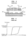
- the spatial light modulator is embodied by a reflective deformable grating light modulator 10 as shown in FIG. 1 .
- the modulator 10 is disclosed in U.S. Pat. No. 5,311,360 by Bloom et al.
- the modulator 10 includes a plurality of reflective deformable ribbons 18, which have reflective surface parts, are suspended above an upper part of a silicon substrate 16, and are spaced apart from each other at regular intervals.
- An insulating layer 11 is deposited on the silicon substrate 16. Subsequently, a sacrificial silicon dioxide film 12 and a low-stress silicon nitride film 14 are deposited.
- the nitride film 14 is patterned by the ribbons 18, and a portion of the silicon dioxide film 12 is etched, thereby maintaining the ribbons 18 on the oxide spacer layer 12 by a nitride frame 20.
- the modulator is designed so that thicknesses of the ribbon 18 and oxide spacer 12 are each ⁇ /4.
- a grating amplitude of the modulator 10 is controlled by applying a voltage between the ribbon 18 (the reflective surface 22 of the ribbon 18 acting as a first electrode) and the substrate 16 (a conductive layer 24 formed on a lower side of the substrate 16 to act as a second electrode).
- the grating amplitude is ⁇ /2 while a total round-trip path difference between light beams reflected from the ribbon and substrate is ⁇ o .
- the modulator 10 acts as a plane mirror when it reflects incident light.
- reference numeral 20 denotes the incident light reflected by the modulator 10 in the undeformed state.
- the electrostatic force enables the ribbon 18 to move downward toward the surface of the substrate 16.
- the grating amplitude is changed to ⁇ /4.
- the total round-trip path difference is a half of a wavelength, and light reflected from the deformed ribbon 18 and light reflected from the substrate 16 are subjected to destructive interference.
- the modulator diffracts incident light 26 using the interference.
- reference numerals 28 and 30 denote light beams diffracted in +/- diffractive modes (D +1 , D -1 ) in the deformed state, respectively.
- FIG. 4 is a graph illustrating light output (which indirectly indicates the deformation of the ribbon 18) as a function of a voltage between the ribbon 18 and substrate 16, which shows an induced hysteretic characteristic. Accordingly, when the ribbon 18 is deformed into a down position to come into contact with the substrate 16, they are latched and require a holding voltage smaller than the original applied voltage.
- U.S. Pat. No. 5,311,360 by Bloom et al. discloses a latching feature which gives a modulator 10 advantages of an active matrix design without the need for active components. Additionally, Bloom et al. describes that this feature is valuable in low power applications where efficient use of available power is very important. However, Bloom et al. discloses the addition of small ridges below ribbons 18 to reduce a contact area, thereby reducing the sticking problem. However, since the substrate of the modulator 10 is used as an optical surface, a process of adding the small ridges to the surface is complicated in that a reflective element of the substrate 16 must be smooth so as to have high reflectance and must be positioned on a planar surface of the ribbon 18.
- Typical display devices are formed in 2-D arrays of pixels. Discontinuous images formed by a plurality of pixels are integrated by user's eyes, thereby forming an aggregate image of pixels constituting a whole image. Unfortunately, prices of such a display device are high because the pixels are overlapped to form a complete array, so the production cost of each pixel is duplicated.
- the display device comprising pixels is exemplified by televisions or computer systems. Their pixels may be formed by an LCD device or a CRT device.
- a diffractive grating light valve capable of reducing or removing the sticking between the reflective element and the substrate without a complicated surface treatment adopted to reduce the sticking.
- a display device which reduces the number of pixels to reduce production costs without reducing image quality while designing a system.
- Korean Pat. Application No. 10-2000-7014798 entitled “method and device for modulating incident light beam to form 2-D image", by Silicon Light Machines Inc.
- the diffractive grating light valve includes a plurality of elongate elements each having a reflective surface.
- the elongate elements are arranged on an upper side of a substrate so that they are parallel to each other, have support ends, and their reflective surfaces lie in array (GLV array).
- the elongate elements form groups according to display elements. The groups alternately apply a voltage to the substrate, resulting in deformation of the elements.
- the almost planar center portion of each deformed elongate element is parallel to and spaced from the center portion of the undeformed element by a predetermined distance which is set to 1/3 - 1/4 of the distance between the undeformed reflective surface and the substrate.
- the deformed elongate elements are prevented from coming into contact with the surface of the substrate. Sticking between the elongate elements and the substrate is prevented by preventing contact between the elements and substrate. Additionally, the predetermined distance between each deformed elongate element and the substrate is limited so as to prevent hysteresis causing deformation of the elongate elements.
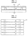
- FIG. 5 is a side sectional view of an elongate element 100 of a GLV in an undeformed state according to a conventional improved technology.
- the elongate element 100 is suspended above a surface of a substrate (including constitution layers) by ends thereof.
- reference numeral 102 denotes an air space.
- FIG. 6 is a plan view of a portion of the GLV including six elongate elements 100.
- the elongate elements 100 have the same width and are arranged parallel to each other.
- the elongate elements 100 are spaced close to each other, so that the elongate elements 100 can be deformed independently from other elements.
- the six elongate elements 100 as shown in FIG. 6 preferably form a single display element 200. Therefore, an array of 1920 elongate elements forms a GLV array having 320 display devices arranged therein.
- FIG. 7 is a front sectional view of a display element 200 having undeformed elongate elements 100.
- FIG. 7 is a view taken along the line A-A' of FIG. 5 .
- the undeformed state is selected by equalizing a bias on the elongate elements 100 to a conductive layer 106. Since reflective surfaces of the elongate elements 100 are substantially coplanar, light incident on the elongate elements 100 is reflected.
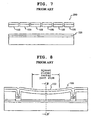
- FIG. 8 is a side sectional view of a deformed elongate element 100 of the GLV.
- FIG. 8 shows that the deformed elongate element 100 is maintained in the suspended state thereof to be spaced from the surface of the substrate adjacent therebeneath. This is in contrast to the conventional modulator of FIGS. 1 to 3 . Contact between the elongate element 100 and the surface of the substrate is prevented, thereby avoiding the disadvantages of conventional modulators. However, the elongate element 100 is apt to sag in the deformed state.
- the elongate element 100 is uniformly subjected to an electrostatic attractive force acting toward the substrate in directions perpendicular to a longitudinal direction thereof, whereas tension of the elongate element 100 acts along the length of the elongate element 100. Therefore, the reflective surface of the elongate element is not planar but curvilinear.
- the center part 102 of the elongate element 100 ( FIG. 8 ) is almost planar, making the contrast ratio of diffracted light, gained by only the center part 102 of the elongate element 100, desirable.
- the substantially planar center part 102 has a length that is 1/3 of a distance between post holes 110. Hence, when the distance between the post holes 110 is 75 ⁇ m, the almost planar center part 102 is about 25 ⁇ m long.
- FIG. 9 is a front view of the display element 200 in which the deformed elongate elements 100 are alternately arranged.
- FIG. 9 is a view taken in the direction of the arrows along the line B-B' of FIG. 8 .
- the elongate ribbons 100 which are not removed are maintained at desired positions by an applied bias voltage. Deformation of the moving elongate ribbons 100 is achieved by alternate applications of operation voltages through the conductive layer 106 to the elongate elements 100.
- a vertical distance (d 1 ) is almost constant to the almost planar center part 102 ( FIG. 8 ), thereby limiting the grating amplitude of the GLV.
- the grating amplitude (d 1 ) may be controlled by adjusting an operation voltage on the operated elongate elements 100. This results in precision tuning of the GLV in an optimum contrast ratio.
- the GLV has a grating width (d 1 ) that is 1/4 ( ⁇ /4) of the wavelength of incident light to assure a maximum contrast ratio in an image to be display deviceed.
- each elongate element 100 is spaced upward from the substrate by a distance of d 2 . Accordingly, the elongate elements 100 do not come into contact with the substrate during operation of the GLV. This results in avoidance of the sticking problems between the reflective ribbons and the substrate occurring in conventional modulators.
- the light modulator which is manufactured by Silicon Light Machines Inc. and adopts an electrostatic method to control the position of a micromirror is disadvantageous in that an operation voltage is relatively high (usually 30 V or so) and a correlation between the applied voltage and a displacement is nonlinear, and thus, reliability is poor in the course of controlling light.
- US 2002/0167245 A1 discloses a method of redirecting light using an actuatable two-layer diffraction grating structure having actuating beams of the diffractive optical element being supported over a substrate and supporting a corresponding one of the grating elements over the substrate to form a corresponding auxiliary gap.
- the grating elements may be actuated piezoelectrically.
- WO 03/014789 A discloses a microsystem switch having a support defining a recess and a flexible, prestressed, bistable bridge being mounted on the support bridging the recess, wherein the bridge is shaped so as to hold selectively a concave support stable state, in which the bridge bulges out of the recess.
- the switch includes an actuator for effecting flexing of the bridge between the two stable states and a switching element is mounted on the bridge such that movement of the bridge between the stable states moves the switching element between an on position and an off position. An optical path is blocked or opened by the movement of the switching element. Actuation may be performed using a piezoelectric effect
- WO 01/13457 A1 discloses an electrical switch with a deformable cantilever having a piezoelectric material and FR 2 753 565 discloses a flexible membrane with a piezoelectrical layer and thus both are further away.
- an object of the present invention is to provide a diffractive thin-film piezoelectric micromirror, which is operated by a piezoelectric operation method, unlike a conventional reflective diffractive light modulator operated by an electrostatic operation method, to assure excellent displacement, operation speed, reliability, linearity, and low voltage operation, and a method of producing the same.
- Another object of the present invention is to provide a diffractive thin-film piezoelectric micromirror, which is operated by a thin-film piezoelectric operation method to make various structure designs on a silicon wafer possible, and a method of producing the same.
- a diffractive thin-film piezoelectric micromirror device including a substrate on which a recess is formed to provide an air space to the center thereof. It also comprises a lower supporter having a ribbon shape, which is attached to the substrate along both ends of the recess at both ends thereof while being spaced from the bottom of the recess at the center portion thereof and which includes a thin-film piezoelectric material layer to be vertically movable at the center portion thereof when voltage is applied to the piezoelectric material layer, and thus diffracts an incident light beam.
- the present invention provides a diffractive thin-film piezoelectric micromirror, including a substrate on which a recess is formed to provide an air space to the center thereof; a lower supporter which has a ribbon shape, is attached to an upper side of the substrate along both ends of the recess at both ends thereof while being spaced from the bottom of the recess at a center portion thereof, the center portion being vertically movable; and a piezoelectric mirror layer having a ribbon shape, which is laminated on the lower supporter while being spaced from the bottom of the recess of the substrate at both ends thereof and which includes a thin-film piezoelectric material layer to be vertically movable when voltage is applied to both sides of the thin-film piezoelectric material layer, and thus diffracts an incident light beam.
- the present invention provides a diffractive thin-film piezoelectric micromirror, including a substrate on which a recess is formed to provide an air space to the center thereof; a lower supporter which has a ribbon shape, and is attached to an upper side of the substrate along both ends of the recess at both ends thereof while being spaced from the bottom of the recess at a center portion thereof; a first piezoelectric layer which is positioned on an end of the lower supporter at an end thereof and at a location far from a center of the lower supporter toward the end of the lower supporter by a predetermined distance at the other end thereof, and which includes a first thin-film piezoelectric material layer to shrink and expand so as to provide a first vertical actuating force when voltage is applied to the first thin-film piezoelectric material layer; a second piezoelectric layer which is positioned on the other end of the lower supporter at an end thereof and at a location far from the center of the lower supporter toward the other end of the lower supporter by
- the present invention provides a diffractive thin-film piezoelectric micromirror, including a substrate on which an insulating layer is formed; a lower supporter which has a ribbon shape and is attached to the substrate at both ends thereof while being spaced from the substrate at the center portion thereof by a predetermined distance, the center portion being vertically movable; and a piezoelectric mirror layer which is laminated on the lower supporter while being spaced from the substrate at the center portion thereof, and includes a thin-film piezoelectric material layer to shrink and expand so as to vertically move at the center portion thereof when a voltage is applied to the piezoelectric material layer, and diffracting an incident light beam.
- the present invention provides a diffractive thin-film piezoelectric micromirror, including a substrate on which an insulating layer is formed; a lower supporter which has a ribbon shape and is attached to both ends of the substrate at both ends thereof while being spaced from the substrate at the center portion thereof by a predetermined distance, the center portion being vertically movable; a first piezoelectric layer which is positioned on an end of the lower supporter at an end thereof and at a location far from the center of the lower supporter toward the end of the lower supporter by a predetermined distance at the other end thereof, and which includes a thin-film piezoelectric material layer to shrink and expand so as to be vertically moved when voltage is applied to the piezoelectric material layer; a second piezoelectric layer which is positioned on the other end of the lower supporter at an end thereof and at a location far from the center of the lower supporter toward the other end of the lower supporter by a predetermined distance at the other end thereof, and shrinks and expands so as to to
- the present invention provides a method of producing such a diffractive thin-film piezoelectric micromirror device according to claim 5.
- the present invention provides a method of producing a diffractive thin-film piezoelectric micromirror, including a first step of forming a mask layer on a silicon wafer and patterning the mask layer to form a recess; a second step of forming a sacrificial layer so as to fill the recess formed in the first step; a third step of forming a lower supporter on a silicon substrate in which the recess is filled; a fourth step of forming a pair of piezoelectric mirror layers on the lower supporter formed in the third step in such a way that each of the piezoelectric mirror layers is positioned on the remaining portion of the substrate other than the recess at an end thereof and at a location far from the center of the recess outward by a predetermined distance at the other end thereof, and the piezoelectric mirror layers are opposite to each other; a fifth step of forming a micromirror layer on the center portion of the lower supporter; and a sixth step of etching a pair of
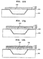
- FIGS. 10a to 10j a micromirror device
- FIGS. 10a to 10j illustrate production of a diffractive thin-film piezoelectric micromirror having a recess.
- a mask layer 1002 is formed in a thickness of 0.1 - 1.0 ⁇ m through a thermal oxidation process on a silicon wafer 1001, and then patterned for silicon etching.
- the silicon is etched in a predetermined thickness, using a solution capable of etching the silicon, such as TMAH or KOH, and the mask layer 1002 is then removed.
- a solution capable of etching the silicon such as TMAH or KOH
- an insulating and etching prevention layer 1003 is formed on the etched silicon according to the thermal oxidation process. That is to say, the insulating and etching prevention layer 1003, such as SiO 2 is formed on a surface of the silicon wafer.
- a polysilicon (Poly-Si) or an amorphous-Si is deposited on an etched portion of the silicon wafer 1001 according to low pressure chemical vapor deposition (LPCVD) or plasma chemical vapor deposition (PECVD) processes to form a sacrificial layer 1004 for an air space, and the resulting silicon wafer is polished to be flattened at a surface thereof.
- LPCVD low pressure chemical vapor deposition
- PECVD plasma chemical vapor deposition
- SOI silicon on insulator
- silicon nitrides such as Si 3 N 4
- SiO 2 is deposited in a thickness of 0.1 - 5 ⁇ m according to thermal oxidation or PECVD processes, but this procedure may be omitted according to necessity.
- a lower supporter 1005 for supporting the piezoelectric material is deposited on the silicon wafer 1001.
- a material constituting the lower supporter 1005 may be exemplified by Si oxides (e.g. SiO 2 , etc.), Si nitrides (e.g. Si 3 N 4 , etc.), ceramic substrates (Si, ZrO 2 , Al 2 O 3 and the like), and Si carbides.
- the lower supporter 1005 may be omitted, if necessary.
- a lower electrode 1006 is formed on the lower supporter 1005, in which examples of material for the lower electrode 1006 may include Pt, Ta/Pt, Ni, Au, Al, RuO 2 and the like.
- the material is deposited in a thickness of 0.01 - 3 ⁇ m using sputtering or evaporation processes.
- a piezoelectric material 1007 is formed in a thickness of 0.01 - 20.0 ⁇ m on the lower electrode 1006 according to a wet process (screen printing, sol-gel coating and the like) or a dry process (sputtering, evaporation, vapor deposition and the like). Both longitudinal type and transverse type piezoelectric materials may be used as the piezoelectric material 1007. Examples of the piezoelectric material may include PzT, PNN-PT, ZnO and the like, and the piezoelectric electrolytic material contains at least one selected from the group consisting of Pb, Zr, Zn, or titanium.
- an upper electrode 1008 is formed on the piezoelectric material 1007, in which a material of the upper electrode may be exemplified by Pt, Ta/Pt, Ni, Au, Al, and RuO 2 .
- the upper electrode is formed in a thickness of 0.01 - 3 ⁇ m using the sputtering or evaporation processes.
- a micromirror 1009 is attached to the upper electrode 1008, in which examples of a material of the micromirror include a light-reflective material, such as Ti, Cr, Cu, Ni, Al, Au, Ag, Pt, and Au/Cr.
- a light-reflective material such as Ti, Cr, Cu, Ni, Al, Au, Ag, Pt, and Au/Cr.
- the upper electrode 1008 may be used as the micromirror, or a separate micromirror may be deposited on the upper electrode 1008.
- the micromirror 1009, upper electrode 1008, piezoelectric material 1007, lower electrode 1006, and lower supporter 1005 are etched to form the diffractive thin-film piezoelectric micromirror array.
- the sacrificial layer 1004 is etched using XeF 2 gas.
- the micromirror array may be formed after the sacrificial layer 1004 is removed.
- a hole is formed in a portion of the mother body of the diffractive thin-film piezoelectric micromirror array, on which the lower supporter 1005 is not formed, and the sacrificial layer 1004 is etched using XeF 2 gas. Subsequently, the mother body of the diffractive thin-film piezoelectric micromirror array is patterned using the mask layer, such as the photoresist, and the micromirror 1009, upper electrode 1008, piezoelectric material 1007, lower electrode 1006, and lower supporter 1005 are etched to form the micromirror array.
- the mask layer such as the photoresist
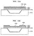
- FIGS. 11a to 11c illustrate various diffractive thin-film piezoelectric micromirrors having recesses, in which piezoelectric materials are not deformed.
- FIG. 11a illustrates that a sacrificial layer of a silicon wafer is replaced with an air space, and thus, a piezoelectric material is partially spaced from a surface of a substrate and supported by ends thereof. Additionally, a lower electrode 1006a, a piezoelectric material layer 1007a, an upper electrode 1008a, and a micromirror 1009a are positioned on a lower supporter 1005a.
- FIG. 11b as preferred embodiment of the invention illustrates that a sacrificial layer of a silicon wafer is replaced with an air space, and thus, a piezoelectric material is partially spaced from a surface of a substrate and supported by ends thereof.
- a micromirror 1009b is positioned on the center part of a lower supporter 1005b.
- a lower electrode 1006b, a piezoelectric material layer 1007b, and an upper electrode 1008b are positioned on both ends of a lower supporter 1005b.
- the center portions of the lower electrode 1006b, piezoelectric material layer 1007b, and upper electrode 1008b are etched, and the micromirror 1009b is then formed on the center part.
- FIG. 11c illustrates that a sacrificial layer of a silicon wafer is replaced with an air space, and thus, a piezoelectric material is partially spaced from a surface of a substrate and supported by ends thereof.
- a lower electrode 1006c, a piezoelectric material layer 1007c, an upper electrode 1008c, and a micromirror 1009c are positioned on the center part of a lower supporter 1005c.
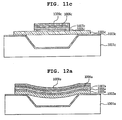
- FIGS. 12a to 12c illustrate various diffractive thin-film piezoelectric micromirrors having recesses, in which piezoelectric materials are deformed.
- FIG. 12a shows that when voltage is applied to upper and lower parts of a piezoelectric material 1007a, a lower supporter 1005a, a lower electrode 1006a, a piezoelectric material layer 1007a, an upper electrode 1008a, and a micromirror 1009a are warped downward by contractile and expansive forces of the piezoelectric material.
- the contractile force acts on the piezoelectric material 1007a in a horizontal direction, causing the piezoelectric material 1007a to shrink in a horizontal direction.
- the contractile force causes the piezoelectric material 1007a to be warped downward.
- FIG. 12b referring to a preferred embodiment of the invention shows that when voltage is applied to upper and lower sides of a piezoelectric material layer 1007b positioned on both ends of a lower supporter 1005b, a contractile force is generated in a horizontal direction. At this time, the contractile force acts on the piezoelectric material 1007b in the horizontal direction, causing the piezoelectric material 1007b to shrink in the horizontal direction. However, since a lower side of the piezoelectric material 1007b is firmly attached to the lower supporter 1005b, the contractile force causes the piezoelectric material 1007b to be warped upward. As a result, the lower supporter 1005b and a micromirror 1009b positioned on the center of the lower supporter 1005b are warped upward.
- FIG. 12c shows that when voltage is applied to upper and lower sides of a piezoelectric material 1007c positioned on the center of a lower supporter 1005c, a lower electrode 1006c, a piezoelectric material layer 1007c, an upper electrode 1008c, and a micromirror 1009c are warped upward.
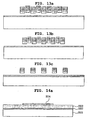
- FIG. 13a illustrates operation of a display element in which diffractive thin-film piezoelectric micromirrors having recesses and the same dimensions are arranged.
- the diffractive thin-film piezoelectric micromirrors are vertically moved by the application of voltage.
- FIG. 13b illustrates operation of a display element in which diffractive thin-film piezoelectric micromirrors having recesses and different dimensions are alternately arranged.
- the diffractive thin-film piezoelectric micromirrors are vertically moved by the application of voltage.
- FIG. 13c illustrates operation of a display element in which diffractive thin-film piezoelectric micromirrors having recesses and the same dimension are arranged. At this time, the micromirrors are formed on a whole upper side of an insulating layer to diffract incident light.
- FIGS. 14a to 14h illustrate production of a thin-film piezoelectric light modulator having a raised part.
- an insulating and etching prevention layer 2002 is formed on a silicon wafer according to the thermal oxidation process. That is to say, the insulating and etching prevention layer 2002 made of SiO 2 is formed on a surface of the silicon wafer.
- a polysilicon (Poly-Si) or an amorphous-Si is deposited on the insulating and etching prevention layer 2002 of the silicon wafer 2001 according to LPCVD or PECVD processes to form an air space, and the resulting silicon wafer is polished to be flattened at a surface thereof to form a sacrificial layer 2003.
- a mask layer 2004 is formed in a thickness of 0.1 - 3.0 ⁇ m through a thermal oxidation process on the sacrificial layer 2003, and then patterned for silicon etching.
- silicon is etched using a solution capable of etching silicon, such as TMAH or KOH, in a predetermined thickness, and the mask layer 2004 is then removed.
- a solution capable of etching silicon such as TMAH or KOH
- SiO 2 is deposited in a thickness of 0.1 - 3 ⁇ m according to thermal oxidation or PECVD processes, but this procedure may be omitted according to necessity.
- a lower supporter 2005 for supporting a piezoelectric material is deposited on the insulating and etching prevention layer 2002 and sacrificial layer 2003.
- a material constituting the lower supporter 2005 may be exemplified by Si oxides (e.g. SiO 2 , etc.), Si nitrides (e.g. Si 3 N 4 , etc.), ceramic substrates (e.g. Si, ZrO 2 , Al 2 O 3 and the like), and Si carbides.
- the lower supporter 2005 may be omitted, if necessary.
- a lower electrode 2006 is formed on the lower supporter 2005, in which examples of material for the lower electrode 2006 may include Pt, Ta/Pt, Ni, Au, Al, RuO 2 and the like, and the material is deposited in a thickness of 0.01 - 3 ⁇ m using sputtering or evaporation processes.
- a piezoelectric material 2007 is formed in a thickness of 0.01 - 20.0 ⁇ m on the lower electrode 2006 according to a wet process (screen printing, sol-gel coating and the like) or a dry process (sputtering, evaporation, vapor deposition and the like). Both longitudinal type and transverse type piezoelectric materials may be used as the piezoelectric material 2007. Examples of the piezoelectric material may include PZT, PMN-PT, PLZT, AIN, ZnO and the like, and the piezoelectric electrolytic material contains at least one selected from the group consisting of Pb, Zr, Zn, or titanium.
- an upper electrode 2008 is formed on the piezoelectric material 2007, in which a material of the upper electrode may be exemplified by Pt, Ta/Pt, Ni, Au, Al, Ti/Pt, IrO 2 and RuO 2 and the upper electrode is formed in a thickness of 0.01 - 3 ⁇ m using the sputtering or evaporation processes.
- a material of the upper electrode may be exemplified by Pt, Ta/Pt, Ni, Au, Al, Ti/Pt, IrO 2 and RuO 2 and the upper electrode is formed in a thickness of 0.01 - 3 ⁇ m using the sputtering or evaporation processes.
- a micromirror 2009 is attached to the upper electrode 2008.
- a material of the micromirror include a light-reflective material, such as Ti, Cr, Cu, Ni, Al, Au, Ag, Pt, and Au/Cr.
- the upper electrode 2008 may be used as the micromirror, or a separate micromirror may be deposited on the upper electrode 2008.
- the micromirror 2009, upper electrode 2008, piezoelectric material 2007, lower electrode 2006, and lower supporter 2005 are etched to form the diffractive thin-film piezoelectric micromirror array.
- the sacrificial layer 2003 is etched using XeF 2 gas.
- the micromirror array may be formed after the sacrificial layer 2003 is removed.
- a hole is formed in a portion of the mother body of the diffractive thin-film piezoelectric micromirror array, in which the lower supporter 2005 is not formed, the sacrificial layer 2003 is etched using XeF 2 gas.
- the mother body of the diffractive thin-film piezoelectric micromirror array is patterned using the mask layer, such as the photoresist, and the micromirror 2009, upper electrode 2008, piezoelectric material 2007, lower electrode 2006, and lower supporter 2005 are etched to form the micromirror array.
- FIGS. 15a to 15c illustrate various diffractive thin-film piezoelectric micromirrors having raised parts, in which piezoelectric materials are not deformed.
- FIG. 15a illustrates that a sacrificial layer of a silicon wafer is replaced with an air space, and thus, a piezoelectric material is partially spaced from a surface of a substrate and supported by ends thereof. Additionally, a lower electrode 2006a, a piezoelectric material layer 2007a, an upper electrode 2008a, and a micromirror 2009a are positioned on a lower supporter 2005a. FIG. 15a is different from FIG. 11a in that a portion of the piezoelectric material is raised upward and spaced from an insulating and etching prevention layer.
- FIG. 15b illustrates that a sacrificial layer of a silicon wafer is replaced with an air space, and thus, a piezoelectric material is partially spaced from a surface of a substrate and supported by ends thereof.
- a micromirror 2009b is positioned on the center part of a lower supporter 2005b.
- a lower electrode 2006b, a piezoelectric material layer 2007b, and an upper electrode 2008b are positioned on both ends of the lower supporter 2005b.
- FIG. 15b is different from FIG. 11b in that a portion of the piezoelectric material is raised upward and spaced from an insulating and etching prevention layer.
- FIG. 15c illustrates that a sacrificial layer of a silicon wafer is replaced with an air space, and thus, a piezoelectric material is partially spaced from a surface of a substrate by ends thereof.
- a lower electrode 2006c, a piezoelectric material layer 2007c, an upper electrode 2008c, and a micromirror 2009c are positioned on the center part of a lower supporter 2005c.
- FIG. 15c is different from FIG. 11c in that a portion of the piezoelectric material is raised upward and spaced from an insulating and etching prevention layer.
- FIGS. 16a to 16c illustrate various diffractive thin-film piezoelectric micromirrors having raised parts, in which piezoelectric materials are deformed.
- FIG. 16a shows that when voltage is applied to upper and lower sides of a piezoelectric material 2007a, a lower supporter 2005a, a lower electrode 2006a, a piezoelectric material layer 2007a, an upper electrode 2008a, and a micromirror 2009a are warped downward by contractile and expansive forces of the piezoelectric material.
- the contractile force acts on the piezoelectric material 2007a in a horizontal direction, endeavoring the piezoelectric material 2007a to shrink in a horizontal direction.
- the contractile force causes the piezoelectric material 2007a to be warped downward.
- FIG. 16b shows that when voltage is applied to upper and lower sides of a piezoelectric material layer 2007b positioned on both ends of a lower supporter 2005b, a contractile force is generated in a horizontal direction. At this time, the contractile force acts on the piezoelectric material 2007b in the horizontal direction, causing the piezoelectric material 2007b to shrink in the horizontal direction. However, since a lower side of the piezoelectric material 2007b is firmly attached to the lower supporter 2005b, the contractile force enables the piezoelectric material 2007b to be warped upward. As a result, the lower supporter 2005b and a micromirror 2009b positioned on the center of the lower supporter 2005b are warped upward.
- FIG. 16c shows that when voltage is applied to upper and lower parts of a piezoelectric material 2007c positioned on the center of a lower supporter 2005c, a lower electrode 2006c, a piezoelectric material layer 2007c, an upper electrode 2008c, and a micromirror 2009c are warped upward.
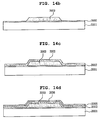
- FIG. 17a illustrates operation of a display element in which diffractive thin-film piezoelectric micromirrors having raised parts and the same width are arranged.
- the diffractive thin-film piezoelectric micromirrors are vertically moved by the application of voltage.
- FIG. 17b illustrates operation of a display element in which diffractive thin-film piezoelectric micromirrors having raised parts and different widths are alternately arranged.
- the diffractive thin-film piezoelectric micromirrors are vertically moved by the application of voltage.
- FIG. 17c illustrates operation of a display element in which diffractive thin-film piezoelectric micromirrors having raised parts are arranged at regular intervals.
- the micromirrors are formed on an upper side of an insulating layer to diffract incident light.
- the specification of the present invention describes only a piezoelectric material layer consisting of a single layer, but the piezoelectric material layer may comprise multiple layers so as to realize low voltage operation. At this time, the lower and upper electrodes consist of multiple layers.
- first lower electrode, a first piezoelectric material layer, a first upper electrode, a second lower electrode, a second piezoelectric material layer, a second upper electrode, a third lower electrode . . . are sequentially laminated upward.
- the present invention is advantageous in that it is possible to gain the desired displacement at a relatively low voltage and to gain a high operation speed.
- Another advantage of the present invention is that since it is possible to reliably control displacement of a ribbon, it is possible to achieve a gray scale control unlike the electrostatic method.
Landscapes
- Physics & Mathematics (AREA)
- Engineering & Computer Science (AREA)
- General Physics & Mathematics (AREA)
- Theoretical Computer Science (AREA)
- Optics & Photonics (AREA)
- Microelectronics & Electronic Packaging (AREA)
- Manufacturing & Machinery (AREA)
- Computer Hardware Design (AREA)
- Chemical & Material Sciences (AREA)
- Ceramic Engineering (AREA)
- Mechanical Light Control Or Optical Switches (AREA)
- Micromachines (AREA)
- General Electrical Machinery Utilizing Piezoelectricity, Electrostriction Or Magnetostriction (AREA)
Applications Claiming Priority (2)
| Application Number | Priority Date | Filing Date | Title |
|---|---|---|---|
| KR2003077389 | 2003-11-03 | ||
| KR20030077389 | 2003-11-03 |
Publications (2)
| Publication Number | Publication Date |
|---|---|
| EP1528038A1 EP1528038A1 (en) | 2005-05-04 |
| EP1528038B1 true EP1528038B1 (en) | 2009-09-23 |
Family
ID=34420705
Family Applications (1)
| Application Number | Title | Priority Date | Filing Date |
|---|---|---|---|
| EP20040023723 Expired - Fee Related EP1528038B1 (en) | 2003-11-03 | 2004-10-05 | Diffractive thin-film piezoelectric micromirror and method of producing the same |
Country Status (6)
| Country | Link |
|---|---|
| US (1) | US7626745B2 (ko) |
| EP (1) | EP1528038B1 (ko) |
| JP (1) | JP2005141208A (ko) |
| KR (1) | KR100645640B1 (ko) |
| CN (1) | CN1614458B (ko) |
| DE (1) | DE602004023264D1 (ko) |
Families Citing this family (18)
| Publication number | Priority date | Publication date | Assignee | Title |
|---|---|---|---|---|
| KR100632606B1 (ko) * | 2004-08-19 | 2006-10-09 | 삼성전기주식회사 | 색선별 슬릿을 이용한 광변조기 다중광 스캐닝 장치 |
| US7215461B1 (en) * | 2004-09-14 | 2007-05-08 | Silicon Light Machines Corporation | MEMS devices with increased damping for suspended movable structures |
| KR100897671B1 (ko) * | 2005-02-04 | 2009-05-14 | 삼성전기주식회사 | 회절형 광변조기 |
| KR100832622B1 (ko) * | 2005-05-25 | 2008-05-27 | 삼성전기주식회사 | 광변조기 및 그 광변조기를 이용한 프로젝터를 구비한휴대용 단말기 |
| KR100859003B1 (ko) * | 2005-11-01 | 2008-09-18 | 삼성전기주식회사 | 알루미늄 합금을 이용한 광 반사층을 갖는 광변조기 소자및 그 제조 방법 |
| KR100781367B1 (ko) * | 2005-11-01 | 2007-11-30 | 삼성전기주식회사 | 광반사층 상에 보호막을 갖는 광변조기 소자 |
| DE102006057568A1 (de) * | 2006-11-28 | 2008-05-29 | Micronic Laser Systems Ab | Mikrooptisches Element mit einem Substrat und Verfahren zu seiner Herstellung |
| DE102006057567B4 (de) * | 2006-11-28 | 2008-09-04 | Micronic Laser Systems Ab | Mikrooptisches Element mit einem Substrat, an dem an einer optisch wirksamen Oberfläche mindestens eine Höhenstufe ausgebildet ist, Verfahren zu seiner Herstellung und Verwendungen |
| US7698941B2 (en) * | 2007-06-20 | 2010-04-20 | Headway Technologies, Inc. | Sensing unit and method of making same |
| NO333724B1 (no) * | 2009-08-14 | 2013-09-02 | Sintef | En mikromekanisk rekke med optisk reflekterende overflater |
| JP5703440B2 (ja) * | 2010-07-09 | 2015-04-22 | 株式会社ユーテック | 圧電体回折格子、プロジェクター、発光装置及び表示装置 |
| KR102065107B1 (ko) * | 2013-05-20 | 2020-02-12 | 삼성디스플레이 주식회사 | 무마스크 노광 장치 |
| JP6225544B2 (ja) * | 2013-07-31 | 2017-11-08 | 株式会社デンソー | 圧電素子の製造方法 |
| JP5857342B2 (ja) * | 2014-07-17 | 2016-02-10 | 株式会社ユーテック | 発光装置及び表示装置 |
| US10324173B2 (en) * | 2015-02-13 | 2019-06-18 | Airmar Technology Corporation | Acoustic transducer element |
| WO2017171874A1 (en) * | 2016-04-01 | 2017-10-05 | Intel Corporation | Package-integrated piezoelectric optical grating switch array |
| JP6690419B2 (ja) * | 2016-06-08 | 2020-04-28 | 株式会社デンソー | 半導体光デバイス、および、その製造方法 |
| IT202000001411A1 (it) * | 2020-01-24 | 2021-07-24 | St Microelectronics Srl | Metodo di lavorazione di una fetta per la fabbricazione di una struttura oscillante quale un microspecchio |
Citations (3)
| Publication number | Priority date | Publication date | Assignee | Title |
|---|---|---|---|---|
| US5637517A (en) * | 1995-05-26 | 1997-06-10 | Daewoo Electronics Co., Ltd. | Method for forming array of thin film actuated mirrors |
| EP0831352A1 (en) * | 1996-02-26 | 1998-03-25 | Seiko Epson Corporation | Optical modulating device, display and electronic device |
| US6750901B1 (en) * | 1997-08-11 | 2004-06-15 | Silverbrook Research Pty Ltd | Digital instant printing camera with image processing capability |
Family Cites Families (15)
| Publication number | Priority date | Publication date | Assignee | Title |
|---|---|---|---|---|
| JPH0572490A (ja) | 1991-09-13 | 1993-03-26 | Nippon Telegr & Teleph Corp <Ntt> | 光学装置 |
| US5311360A (en) | 1992-04-28 | 1994-05-10 | The Board Of Trustees Of The Leland Stanford, Junior University | Method and apparatus for modulating a light beam |
| JP2973272B2 (ja) | 1994-05-10 | 1999-11-08 | オムロン株式会社 | 可変光学面及び光スキャニングシステム |
| JP2924738B2 (ja) | 1995-09-29 | 1999-07-26 | オムロン株式会社 | 光偏向装置 |
| JPH09289342A (ja) | 1996-04-19 | 1997-11-04 | Sony Corp | 多層型圧電アクチュエータ |
| FR2753565B1 (fr) | 1996-09-13 | 1998-11-27 | Thomson Csf | Dispositif de commutation electrique et dispositif d'affichage utilisant ce dispositif de commutation |
| US6060818A (en) | 1998-06-02 | 2000-05-09 | Hewlett-Packard Company | SBAR structures and method of fabrication of SBAR.FBAR film processing techniques for the manufacturing of SBAR/BAR filters |
| US6238581B1 (en) | 1998-12-18 | 2001-05-29 | Eastman Kodak Company | Process for manufacturing an electro-mechanical grating device |
| US6724125B2 (en) | 1999-03-30 | 2004-04-20 | Massachusetts Institute Of Technology | Methods and apparatus for diffractive optical processing using an actuatable structure |
| GB2353410B (en) | 1999-08-18 | 2002-04-17 | Marconi Electronic Syst Ltd | Electrical switches |
| JP3979515B2 (ja) | 1999-12-28 | 2007-09-19 | パイオニア株式会社 | 可変光学素子とその可変光学素子を備えたピックアップ装置並びにそのピックアップ装置を備えた情報記録再生装置 |
| JP2002055297A (ja) | 2000-08-11 | 2002-02-20 | Ngk Insulators Ltd | レーザビーム出力装置 |
| JP2002162573A (ja) | 2000-11-24 | 2002-06-07 | Sony Corp | 空間変調器及び画像表示装置 |
| JP4027313B2 (ja) | 2001-07-05 | 2007-12-26 | インターナショナル・ビジネス・マシーンズ・コーポレーション | マイクロシステム・スイッチ |
| JP3852306B2 (ja) | 2001-07-06 | 2006-11-29 | ソニー株式会社 | Mems素子の製造方法、glvデバイスの製造方法、及びレーザディスプレイの製造方法 |
-
2004
- 2004-09-18 KR KR20040074875A patent/KR100645640B1/ko not_active IP Right Cessation
- 2004-09-28 US US10/952,556 patent/US7626745B2/en not_active Expired - Fee Related
- 2004-10-05 DE DE200460023264 patent/DE602004023264D1/de active Active
- 2004-10-05 EP EP20040023723 patent/EP1528038B1/en not_active Expired - Fee Related
- 2004-10-14 JP JP2004300211A patent/JP2005141208A/ja active Pending
- 2004-11-03 CN CN2004100897386A patent/CN1614458B/zh not_active Expired - Fee Related
Patent Citations (3)
| Publication number | Priority date | Publication date | Assignee | Title |
|---|---|---|---|---|
| US5637517A (en) * | 1995-05-26 | 1997-06-10 | Daewoo Electronics Co., Ltd. | Method for forming array of thin film actuated mirrors |
| EP0831352A1 (en) * | 1996-02-26 | 1998-03-25 | Seiko Epson Corporation | Optical modulating device, display and electronic device |
| US6750901B1 (en) * | 1997-08-11 | 2004-06-15 | Silverbrook Research Pty Ltd | Digital instant printing camera with image processing capability |
Non-Patent Citations (2)
| Title |
|---|
| MURALT P: "Ferroelectric thin films for micro-sensors and actuators: a review", JOURNAL OF MICROMECHANICS AND MICROENGINEERING, vol. 10, no. 2, June 2000 (2000-06-01), pages 136 - 146, XP020068545 * |
| WOOD D ET AL: "Actuators and their mechanisms in microengineering", ENGINEERING SCIENCE AND EDUCATION JOURNAL, vol. 7, no. 1, February 1998 (1998-02-01), pages 19 - 27, XP000974919 * |
Also Published As
| Publication number | Publication date |
|---|---|
| US20050105157A1 (en) | 2005-05-19 |
| KR100645640B1 (ko) | 2006-11-15 |
| CN1614458B (zh) | 2010-05-12 |
| KR20050042442A (ko) | 2005-05-09 |
| EP1528038A1 (en) | 2005-05-04 |
| US7626745B2 (en) | 2009-12-01 |
| DE602004023264D1 (de) | 2009-11-05 |
| JP2005141208A (ja) | 2005-06-02 |
| CN1614458A (zh) | 2005-05-11 |
Similar Documents
| Publication | Publication Date | Title |
|---|---|---|
| EP1528038B1 (en) | Diffractive thin-film piezoelectric micromirror and method of producing the same | |
| US6307663B1 (en) | Spatial light modulator with conformal grating device | |
| US7206118B2 (en) | Open hole-based diffractive light modulator | |
| US6663790B2 (en) | Method for manufacturing a mechanical conformal grating device with improved contrast and lifetime | |
| US7133184B2 (en) | Variable grating diffractive light modulator | |
| US7173751B2 (en) | Open hole-based diffractive light modulator | |
| US20050243402A1 (en) | Hybrid light modulator | |
| US20080055710A1 (en) | Diffractive optical modulator | |
| US7209276B2 (en) | Fishbone diffraction-type light modulator | |
| US6977765B1 (en) | Diffractive light modulator using cantilevers | |
| US7289258B2 (en) | Light modulator having variable blaze diffraction grating | |
| US7099064B2 (en) | Electrostatic-type variable diffractive light modulator and manufacturing method thereof | |
| US7382517B2 (en) | Hybrid light modulator | |
| US6594060B2 (en) | Electromechanical conformal grating device with improved optical efficiency and contrast | |
| GB2413647A (en) | Open hole-based diffractive light modulator | |
| KR100632548B1 (ko) | 대칭 형상의 캔티레버를 이용한 회절형 광변조기 | |
| KR100632547B1 (ko) | 캔티레버를 이용한 회절형 광변조기 | |
| KR100861623B1 (ko) | 진동형 회절 광변조기 | |
| KR100815338B1 (ko) | 저전압 구동 회절형 광변조기 | |
| KR20070047205A (ko) | 복수의 패시베이션층을 갖는 광변조기 소자 | |
| KR20050104760A (ko) | 진동형 회절 광 변조기 |
Legal Events
| Date | Code | Title | Description |
|---|---|---|---|
| PUAI | Public reference made under article 153(3) epc to a published international application that has entered the european phase |
Free format text: ORIGINAL CODE: 0009012 |
|
| 17P | Request for examination filed |
Effective date: 20041005 |
|
| AK | Designated contracting states |
Kind code of ref document: A1 Designated state(s): AT BE BG CH CY CZ DE DK EE ES FI FR GB GR HU IE IT LI LU MC NL PL PT RO SE SI SK TR |
|
| AX | Request for extension of the european patent |
Extension state: AL HR LT LV MK |
|
| AKX | Designation fees paid |
Designated state(s): DE FR |
|
| 17Q | First examination report despatched |
Effective date: 20060111 |
|
| GRAP | Despatch of communication of intention to grant a patent |
Free format text: ORIGINAL CODE: EPIDOSNIGR1 |
|
| GRAS | Grant fee paid |
Free format text: ORIGINAL CODE: EPIDOSNIGR3 |
|
| GRAA | (expected) grant |
Free format text: ORIGINAL CODE: 0009210 |
|
| AK | Designated contracting states |
Kind code of ref document: B1 Designated state(s): DE FR |
|
| REF | Corresponds to: |
Ref document number: 602004023264 Country of ref document: DE Date of ref document: 20091105 Kind code of ref document: P |
|
| PLBE | No opposition filed within time limit |
Free format text: ORIGINAL CODE: 0009261 |
|
| STAA | Information on the status of an ep patent application or granted ep patent |
Free format text: STATUS: NO OPPOSITION FILED WITHIN TIME LIMIT |
|
| 26N | No opposition filed |
Effective date: 20100624 |
|
| PGFP | Annual fee paid to national office [announced via postgrant information from national office to epo] |
Ref country code: FR Payment date: 20130912 Year of fee payment: 10 |
|
| PGFP | Annual fee paid to national office [announced via postgrant information from national office to epo] |
Ref country code: DE Payment date: 20130912 Year of fee payment: 10 |
|
| REG | Reference to a national code |
Ref country code: DE Ref legal event code: R119 Ref document number: 602004023264 Country of ref document: DE |
|
| PG25 | Lapsed in a contracting state [announced via postgrant information from national office to epo] |
Ref country code: DE Free format text: LAPSE BECAUSE OF NON-PAYMENT OF DUE FEES Effective date: 20150501 |
|
| REG | Reference to a national code |
Ref country code: FR Ref legal event code: ST Effective date: 20150630 |
|
| PG25 | Lapsed in a contracting state [announced via postgrant information from national office to epo] |
Ref country code: FR Free format text: LAPSE BECAUSE OF NON-PAYMENT OF DUE FEES Effective date: 20141031 |