EP1524686A1 - Verfahren zur Reduzierung des Kontaktwiderstandes von Anschlussbereichen in einem Halbleiterbauelement - Google Patents
Verfahren zur Reduzierung des Kontaktwiderstandes von Anschlussbereichen in einem Halbleiterbauelement Download PDFInfo
- Publication number
- EP1524686A1 EP1524686A1 EP04077815A EP04077815A EP1524686A1 EP 1524686 A1 EP1524686 A1 EP 1524686A1 EP 04077815 A EP04077815 A EP 04077815A EP 04077815 A EP04077815 A EP 04077815A EP 1524686 A1 EP1524686 A1 EP 1524686A1
- Authority
- EP
- European Patent Office
- Prior art keywords
- metal
- region
- atoms
- layer
- silicon
- Prior art date
- Legal status (The legal status is an assumption and is not a legal conclusion. Google has not performed a legal analysis and makes no representation as to the accuracy of the status listed.)
- Withdrawn
Links
Images

Classifications
-
- H—ELECTRICITY
- H10—SEMICONDUCTOR DEVICES; ELECTRIC SOLID-STATE DEVICES NOT OTHERWISE PROVIDED FOR
- H10D—INORGANIC ELECTRIC SEMICONDUCTOR DEVICES
- H10D64/00—Electrodes of devices having potential barriers
- H10D64/01—Manufacture or treatment
- H10D64/013—Manufacture or treatment of electrodes having a conductor capacitively coupled to a semiconductor by an insulator
- H10D64/01302—Manufacture or treatment of electrodes having a conductor capacitively coupled to a semiconductor by an insulator the insulator being formed after the semiconductor body, the semiconductor being silicon
- H10D64/01304—Manufacture or treatment of electrodes having a conductor capacitively coupled to a semiconductor by an insulator the insulator being formed after the semiconductor body, the semiconductor being silicon characterised by the conductor
- H10D64/01316—Manufacture or treatment of electrodes having a conductor capacitively coupled to a semiconductor by an insulator the insulator being formed after the semiconductor body, the semiconductor being silicon characterised by the conductor the conductor comprising a layer of elemental metal contacting the insulator, e.g. Ta, W, Mo or Al
-
- H—ELECTRICITY
- H10—SEMICONDUCTOR DEVICES; ELECTRIC SOLID-STATE DEVICES NOT OTHERWISE PROVIDED FOR
- H10D—INORGANIC ELECTRIC SEMICONDUCTOR DEVICES
- H10D64/00—Electrodes of devices having potential barriers
- H10D64/01—Manufacture or treatment
- H10D64/011—Manufacture or treatment of electrodes ohmically coupled to a semiconductor
- H10D64/0111—Manufacture or treatment of electrodes ohmically coupled to a semiconductor to Group IV semiconductors
- H10D64/0112—Manufacture or treatment of electrodes ohmically coupled to a semiconductor to Group IV semiconductors using conductive layers comprising silicides
-
- H—ELECTRICITY
- H10—SEMICONDUCTOR DEVICES; ELECTRIC SOLID-STATE DEVICES NOT OTHERWISE PROVIDED FOR
- H10D—INORGANIC ELECTRIC SEMICONDUCTOR DEVICES
- H10D64/00—Electrodes of devices having potential barriers
- H10D64/01—Manufacture or treatment
- H10D64/013—Manufacture or treatment of electrodes having a conductor capacitively coupled to a semiconductor by an insulator
- H10D64/01302—Manufacture or treatment of electrodes having a conductor capacitively coupled to a semiconductor by an insulator the insulator being formed after the semiconductor body, the semiconductor being silicon
- H10D64/01304—Manufacture or treatment of electrodes having a conductor capacitively coupled to a semiconductor by an insulator the insulator being formed after the semiconductor body, the semiconductor being silicon characterised by the conductor
- H10D64/01306—Manufacture or treatment of electrodes having a conductor capacitively coupled to a semiconductor by an insulator the insulator being formed after the semiconductor body, the semiconductor being silicon characterised by the conductor the conductor comprising a layer of silicon contacting the insulator, e.g. polysilicon
- H10D64/01308—Manufacture or treatment of electrodes having a conductor capacitively coupled to a semiconductor by an insulator the insulator being formed after the semiconductor body, the semiconductor being silicon characterised by the conductor the conductor comprising a layer of silicon contacting the insulator, e.g. polysilicon the conductor further comprising a non-elemental silicon additional conductive layer, e.g. a metal silicide layer formed by the reaction of silicon with an implanted metal
-
- H—ELECTRICITY
- H10—SEMICONDUCTOR DEVICES; ELECTRIC SOLID-STATE DEVICES NOT OTHERWISE PROVIDED FOR
- H10D—INORGANIC ELECTRIC SEMICONDUCTOR DEVICES
- H10D64/00—Electrodes of devices having potential barriers
- H10D64/01—Manufacture or treatment
- H10D64/013—Manufacture or treatment of electrodes having a conductor capacitively coupled to a semiconductor by an insulator
- H10D64/01302—Manufacture or treatment of electrodes having a conductor capacitively coupled to a semiconductor by an insulator the insulator being formed after the semiconductor body, the semiconductor being silicon
- H10D64/01304—Manufacture or treatment of electrodes having a conductor capacitively coupled to a semiconductor by an insulator the insulator being formed after the semiconductor body, the semiconductor being silicon characterised by the conductor
- H10D64/01306—Manufacture or treatment of electrodes having a conductor capacitively coupled to a semiconductor by an insulator the insulator being formed after the semiconductor body, the semiconductor being silicon characterised by the conductor the conductor comprising a layer of silicon contacting the insulator, e.g. polysilicon
- H10D64/01308—Manufacture or treatment of electrodes having a conductor capacitively coupled to a semiconductor by an insulator the insulator being formed after the semiconductor body, the semiconductor being silicon characterised by the conductor the conductor comprising a layer of silicon contacting the insulator, e.g. polysilicon the conductor further comprising a non-elemental silicon additional conductive layer, e.g. a metal silicide layer formed by the reaction of silicon with an implanted metal
- H10D64/0131—Manufacture or treatment of electrodes having a conductor capacitively coupled to a semiconductor by an insulator the insulator being formed after the semiconductor body, the semiconductor being silicon characterised by the conductor the conductor comprising a layer of silicon contacting the insulator, e.g. polysilicon the conductor further comprising a non-elemental silicon additional conductive layer, e.g. a metal silicide layer formed by the reaction of silicon with an implanted metal the additional conductive layer comprising a silicide layer formed by the silicidation reaction between the layer of silicon with a metal layer which is not formed by metal implantation
-
- H—ELECTRICITY
- H10—SEMICONDUCTOR DEVICES; ELECTRIC SOLID-STATE DEVICES NOT OTHERWISE PROVIDED FOR
- H10D—INORGANIC ELECTRIC SEMICONDUCTOR DEVICES
- H10D64/00—Electrodes of devices having potential barriers
- H10D64/01—Manufacture or treatment
- H10D64/013—Manufacture or treatment of electrodes having a conductor capacitively coupled to a semiconductor by an insulator
- H10D64/01302—Manufacture or treatment of electrodes having a conductor capacitively coupled to a semiconductor by an insulator the insulator being formed after the semiconductor body, the semiconductor being silicon
- H10D64/01304—Manufacture or treatment of electrodes having a conductor capacitively coupled to a semiconductor by an insulator the insulator being formed after the semiconductor body, the semiconductor being silicon characterised by the conductor
- H10D64/01318—Manufacture or treatment of electrodes having a conductor capacitively coupled to a semiconductor by an insulator the insulator being formed after the semiconductor body, the semiconductor being silicon characterised by the conductor the conductor comprising a layer of alloy material, compound material or organic material contacting the insulator, e.g. TiN
- H10D64/0132—Manufacture or treatment of electrodes having a conductor capacitively coupled to a semiconductor by an insulator the insulator being formed after the semiconductor body, the semiconductor being silicon characterised by the conductor the conductor comprising a layer of alloy material, compound material or organic material contacting the insulator, e.g. TiN the conductor being a metallic silicide
-
- H—ELECTRICITY
- H10—SEMICONDUCTOR DEVICES; ELECTRIC SOLID-STATE DEVICES NOT OTHERWISE PROVIDED FOR
- H10D—INORGANIC ELECTRIC SEMICONDUCTOR DEVICES
- H10D84/00—Integrated devices formed in or on semiconductor substrates that comprise only semiconducting layers, e.g. on Si wafers or on GaAs-on-Si wafers
- H10D84/01—Manufacture or treatment
- H10D84/0123—Integrating together multiple components covered by H10D12/00 or H10D30/00, e.g. integrating multiple IGBTs
- H10D84/0126—Integrating together multiple components covered by H10D12/00 or H10D30/00, e.g. integrating multiple IGBTs the components including insulated gates, e.g. IGFETs
- H10D84/0165—Integrating together multiple components covered by H10D12/00 or H10D30/00, e.g. integrating multiple IGBTs the components including insulated gates, e.g. IGFETs the components including complementary IGFETs, e.g. CMOS devices
- H10D84/017—Manufacturing their source or drain regions, e.g. silicided source or drain regions
-
- H—ELECTRICITY
- H10—SEMICONDUCTOR DEVICES; ELECTRIC SOLID-STATE DEVICES NOT OTHERWISE PROVIDED FOR
- H10D—INORGANIC ELECTRIC SEMICONDUCTOR DEVICES
- H10D84/00—Integrated devices formed in or on semiconductor substrates that comprise only semiconducting layers, e.g. on Si wafers or on GaAs-on-Si wafers
- H10D84/01—Manufacture or treatment
- H10D84/0123—Integrating together multiple components covered by H10D12/00 or H10D30/00, e.g. integrating multiple IGBTs
- H10D84/0126—Integrating together multiple components covered by H10D12/00 or H10D30/00, e.g. integrating multiple IGBTs the components including insulated gates, e.g. IGFETs
- H10D84/0165—Integrating together multiple components covered by H10D12/00 or H10D30/00, e.g. integrating multiple IGBTs the components including insulated gates, e.g. IGFETs the components including complementary IGFETs, e.g. CMOS devices
- H10D84/0172—Manufacturing their gate conductors
- H10D84/0174—Manufacturing their gate conductors the gate conductors being silicided
-
- H—ELECTRICITY
- H10—SEMICONDUCTOR DEVICES; ELECTRIC SOLID-STATE DEVICES NOT OTHERWISE PROVIDED FOR
- H10D—INORGANIC ELECTRIC SEMICONDUCTOR DEVICES
- H10D84/00—Integrated devices formed in or on semiconductor substrates that comprise only semiconducting layers, e.g. on Si wafers or on GaAs-on-Si wafers
- H10D84/01—Manufacture or treatment
- H10D84/0123—Integrating together multiple components covered by H10D12/00 or H10D30/00, e.g. integrating multiple IGBTs
- H10D84/0126—Integrating together multiple components covered by H10D12/00 or H10D30/00, e.g. integrating multiple IGBTs the components including insulated gates, e.g. IGFETs
- H10D84/0165—Integrating together multiple components covered by H10D12/00 or H10D30/00, e.g. integrating multiple IGBTs the components including insulated gates, e.g. IGFETs the components including complementary IGFETs, e.g. CMOS devices
- H10D84/0172—Manufacturing their gate conductors
- H10D84/0177—Manufacturing their gate conductors the gate conductors having different materials or different implants
-
- H—ELECTRICITY
- H10—SEMICONDUCTOR DEVICES; ELECTRIC SOLID-STATE DEVICES NOT OTHERWISE PROVIDED FOR
- H10D—INORGANIC ELECTRIC SEMICONDUCTOR DEVICES
- H10D84/00—Integrated devices formed in or on semiconductor substrates that comprise only semiconducting layers, e.g. on Si wafers or on GaAs-on-Si wafers
- H10D84/01—Manufacture or treatment
- H10D84/02—Manufacture or treatment characterised by using material-based technologies
- H10D84/03—Manufacture or treatment characterised by using material-based technologies using Group IV technology, e.g. silicon technology or silicon-carbide [SiC] technology
- H10D84/038—Manufacture or treatment characterised by using material-based technologies using Group IV technology, e.g. silicon technology or silicon-carbide [SiC] technology using silicon technology, e.g. SiGe
-
- H—ELECTRICITY
- H10—SEMICONDUCTOR DEVICES; ELECTRIC SOLID-STATE DEVICES NOT OTHERWISE PROVIDED FOR
- H10D—INORGANIC ELECTRIC SEMICONDUCTOR DEVICES
- H10D30/00—Field-effect transistors [FET]
- H10D30/01—Manufacture or treatment
- H10D30/021—Manufacture or treatment of FETs having insulated gates [IGFET]
- H10D30/0212—Manufacture or treatment of FETs having insulated gates [IGFET] using self-aligned silicidation
-
- H—ELECTRICITY
- H10—SEMICONDUCTOR DEVICES; ELECTRIC SOLID-STATE DEVICES NOT OTHERWISE PROVIDED FOR
- H10P—GENERIC PROCESSES OR APPARATUS FOR THE MANUFACTURE OR TREATMENT OF DEVICES COVERED BY CLASS H10
- H10P14/00—Formation of materials, e.g. in the shape of layers or pillars
- H10P14/40—Formation of materials, e.g. in the shape of layers or pillars of conductive or resistive materials
- H10P14/42—Formation of materials, e.g. in the shape of layers or pillars of conductive or resistive materials using a gas or vapour
- H10P14/43—Chemical deposition, e.g. chemical vapour deposition [CVD]
-
- H—ELECTRICITY
- H10—SEMICONDUCTOR DEVICES; ELECTRIC SOLID-STATE DEVICES NOT OTHERWISE PROVIDED FOR
- H10P—GENERIC PROCESSES OR APPARATUS FOR THE MANUFACTURE OR TREATMENT OF DEVICES COVERED BY CLASS H10
- H10P30/00—Ion implantation into wafers, substrates or parts of devices
- H10P30/20—Ion implantation into wafers, substrates or parts of devices into semiconductor materials, e.g. for doping
- H10P30/202—Ion implantation into wafers, substrates or parts of devices into semiconductor materials, e.g. for doping characterised by the semiconductor materials
- H10P30/204—Ion implantation into wafers, substrates or parts of devices into semiconductor materials, e.g. for doping characterised by the semiconductor materials into Group IV semiconductors
-
- H—ELECTRICITY
- H10—SEMICONDUCTOR DEVICES; ELECTRIC SOLID-STATE DEVICES NOT OTHERWISE PROVIDED FOR
- H10P—GENERIC PROCESSES OR APPARATUS FOR THE MANUFACTURE OR TREATMENT OF DEVICES COVERED BY CLASS H10
- H10P30/00—Ion implantation into wafers, substrates or parts of devices
- H10P30/20—Ion implantation into wafers, substrates or parts of devices into semiconductor materials, e.g. for doping
- H10P30/208—Ion implantation into wafers, substrates or parts of devices into semiconductor materials, e.g. for doping of electrically inactive species
-
- H—ELECTRICITY
- H10—SEMICONDUCTOR DEVICES; ELECTRIC SOLID-STATE DEVICES NOT OTHERWISE PROVIDED FOR
- H10P—GENERIC PROCESSES OR APPARATUS FOR THE MANUFACTURE OR TREATMENT OF DEVICES COVERED BY CLASS H10
- H10P30/00—Ion implantation into wafers, substrates or parts of devices
- H10P30/20—Ion implantation into wafers, substrates or parts of devices into semiconductor materials, e.g. for doping
- H10P30/21—Ion implantation into wafers, substrates or parts of devices into semiconductor materials, e.g. for doping of electrically active species
-
- H—ELECTRICITY
- H10—SEMICONDUCTOR DEVICES; ELECTRIC SOLID-STATE DEVICES NOT OTHERWISE PROVIDED FOR
- H10P—GENERIC PROCESSES OR APPARATUS FOR THE MANUFACTURE OR TREATMENT OF DEVICES COVERED BY CLASS H10
- H10P30/00—Ion implantation into wafers, substrates or parts of devices
- H10P30/20—Ion implantation into wafers, substrates or parts of devices into semiconductor materials, e.g. for doping
- H10P30/224—Ion implantation into wafers, substrates or parts of devices into semiconductor materials, e.g. for doping of a cluster, e.g. using a gas cluster ion beam
Definitions
- the present invention relates to a method for fabricating a semiconductor device having a semiconductor element with at least one connection region, in which the contact resistance of the at least one connection region is reduced and in which unfavourable influences of doping elements are avoided.
- a method for fabricating an IGFET which includes a gate electrode with a low resistance is known from US 5,851,891, which describes the fabrication of an IGFET (insulated gate field-effect transistor) in which the gate electrode of the IGFET is made from silicon and a connection region is formed therein by enabling the silicon to react with a metal applied to it so as to form a metal silicide.
- the silicon of the gate electrode is doped with doping atoms, such as boron atoms. When the metal silicide is being formed, these doping atoms are forced towards the dielectric region without penetrating through it.
- the relatively high doping concentration formed in this way in the vicinity of the dielectric region ensures that an undesirable depletion layer effect does not occur in the gate electrode, since such an effect would increase the effective thickness of the dielectric region.
- the expulsion of doping atoms before the interface of the silicide which is formed is known as the snowplough effect.
- the invention provides a method for fabricating a semiconductor device comprising a semiconductor structure having a silicon region forming at least one connection region in and/or on a substrate having a surface.
- the method comprises forming a metal cluster layer from a first metal over the semiconductor structure or at least over the silicon region thereof.
- This metal cluster layer is formed in such a manner that in the layer metal clusters alternate with sites where there are no metal clusters.
- a non-siliciding metal in other words a metal which is inert with regard to reaction with silicon under the experimental conditions, such as for example W, Mo, Ta, Zr or Nb, is selected for the first metal.
- the method of the invention comprises the deposition of a metal layer of a second metal on top of the metal cluster layer.
- the second metal is a siliciding metal and may, for example, be Ti, Co or Ni. Then, the semiconductor device is subjected to at least one heat treatment in which metal silicide is formed through reaction of the second metal with silicon of the silicon region and in which the atoms of the first metal are displaced in a direction substantially perpendicular to the surface of the substrate, and this as a result of the Kirkendall effect.
- the method according to the invention is characterized in that the metal atoms selected for the atoms of the first metal are different from the second metal, which forms a metal silicide with silicon.
- the metal atoms of the first metal are introduced into or into the vicinity of that region of the regions which form metal silicide whose atoms have the highest diffusion rate during the formation of the metal silicide.
- a semiconductor device having a substrate and a semiconductor body made from silicon.
- the semiconductor body comprises a semiconductor element having at least two semiconductor regions and having a pn junction formed between two of the semiconductor regions which are of opposite conduction types.
- the semiconductor body furthermore comprises at least two electrical connection regions, at least one connection region being formed by a metal region being brought into contact with a silicon region of the semiconductor body and these regions being allowed to react with one another to form a metal silicide which forms part of the connection region, atoms of the metal region and of the silicon region reacting with one another.
- atoms of a material other than silicon or the metal being applied in one of the regions which form metal silicide or between them, in such a manner that these atoms form a region in layer form with interruptions where there are no atoms of the other material, and the atoms of the other material being displaced, during the formation of the metal silicide, in a direction which is perpendicular to the interface between the metal region and the silicon region.
- the method is characterized in that metal atoms of another metal are selected for the atoms of the other material, and the atoms of the other metal are introduced into or into the vicinity of that region of the regions which form metal silicide whose atoms have the highest diffusion rate during the formation of the metal silicide.
- the semiconductor structure may comprise a first main electrode and a second main electrode and a control electrode.
- the first main electrode and second main electrode can be provided with a connection region.
- the control electrode may be provided with a connection region.
- both the first and second main electrodes and the control electrode may be provided with a connection region fabricated as described in the invention.
- the semiconductor structure can be formed as a field-effect transistor having a source region, a drain region and a gate electrode, and the source and drain region and/or gate electrode can be provided with a connection region.
- the first metal can be selected in such a way that its work function is as close as possible to the value desired for the transistor.
- the metal selected has a work function which is as close as possible to the value required for an NMOST, namely approximately 4.2 eV.
- a metal with a work function in the vicinity of approximately 5.2 eV is selected.
- a semiconductor device having at least one NMOS transistor and at least one PMOS transistor can be fabricated.
- the metal cluster layer of the NMOST may be formed from a metal which is different from the metal cluster layer of the PMOST. In this way, it is then possible to obtain different work functions.
- the atoms of the first metal can be applied to the silicon region from the vapour phase in the form of clusters of metal atoms. In this way, openings or sites where there are no clusters are incorporated.
- the atoms of the first metal layer may, as an alternative, be applied by a uniform layer of the first metal being applied to the silicon region of the substrate, and the uniform layer can then be provided with openings.
- the atoms of the first metal can be applied by means of ion implantation.
- the invention provides a semiconductor device having a silicon region and a semiconductor structure with a connection region, the semiconductor device being obtained with the aid of the method of the present invention.
- the semiconductor structure may comprise a first main electrode, a second main electrode and a control electrode.
- the semiconductor structure may be a field-effect transistor having a source region, a drain region and a gate electrode.
- the method of the present invention can be used to fabricate semiconductor structures having a gate electrode 1 and a source and drain region 2, 3.
- the invention is based first of all on the insight that on account of the presence of metal atoms in the vicinity of the dielectric region 25 between a substrate 14 and the gate electrode 1, it is possible, so to speak, to form a metal-containing gate electrode 1. There is then no need or scarcely any need to dope the silicon of the gate electrode 1.
- CMOS IC complementary MOS; contains both n-type and p-type transistors
- the work function of the gate is, according to the invention, controlled by the presence of a metal layer in the border region between the gate electrode 1 and the dielectric region underneath it (see further). Furthermore, the invention is based on the insight that metal atoms can be displaced in silicon in a similar way to doping atoms, but by a significantly different mechanism, namely based on the effect named after Kirkendall.
- the Kirkendall effect is based on the displacement of foreign atoms in a reaction matrix as a result of them being, so to speak, swept through vacancies which, in a matrix of this type, are subject to a displacement in the opposite direction to the direction of the fastest-diffusing component of the reaction matrix.
- the snowplough effect is based on a differing solubility of doping atoms in silicon and in metal silicide. Since the solubility in the metal silicide is much lower than in silicon, the doping atoms are precipitated out of the metal silicide and then pass into the remaining silicon which has not yet reacted. It is important to understand that this effect originates fro an other physical process than the Kirkendall effect. It is caused by the repulsion of the doping atoms by the growing metal component consequent on a too low solubility. The doping atoms are thereby, in case of the snowplough effect, shoved in front of the moving surface of the metal component.
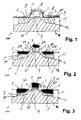
- Figures 1 to 3 diagrammatically depict a cross section through a semiconductor device 100 in successive stages of the fabrication in accordance with a first embodiment of a method according to the invention. Only the most relevant stages are shown in the drawing.
- the starting point for the formation of the device 100 is a semiconductor body 12 (Fig. 1), which in this embodiment of the invention may, for example, be formed from silicon and has a substrate 14, which in this embodiment may likewise be formed from silicon and in which a MOSFET is formed, having a source region 2, a channel region 4 of opposite conduction type to the source region 2, and a drain region 3 of the same conduction type as the source region 2.
- a dielectric region 25 is formed, for example, from silicon dioxide, and above this there is a gate electrode 1, which in the present embodiment may contain polycrystalline silicon.
- the device 100 comprises insulation regions 15, such as for example what are known as trench or LOCOS (locally oxidized silicon) isolations which may, for example, be formed from silicon dioxide.
- LOCOS locally oxidized silicon
- spacers 13 On both sides of the gate electrode 1 there are what are known as spacers 13, which may likewise be formed from silicon dioxide.
- the device 100 is fabricated in a customary way with the aid of generally known techniques, such as LOCOS oxidation, implantation, diffusion, CVD, (plasma) etching and photolithography.
- the surface of the semiconductor body 12 is covered, for example with the aid of chemical vapour deposition (CVD), with a layer of metal clusters 9 formed from a first metal, which may, for example, be tungsten.
- CVD chemical vapour deposition
- the use of chemical vapour deposition means that between the clusters of metal cluster layer 9 there are openings 9A where there is no tungsten, or more generally no first metal.
- These interruptions in the cluster layer 9 consisting of the first metal, which are required for the invention to work successfully, may alternatively in another embodiment also be formed by applying the atoms of the metal cluster layer 9 as a uniform layer of the first metal and then forming openings in this uniform layer. These openings may be formed, for example, with the aid of photolithography and etching.
- small particles of an inert material can be applied to the surface of the semiconductor body 12, after which the atoms of the first metal can then be applied over this surface in the form of a layer.
- the layer of the first metal can then be provided with the desired openings with the aid of a lift-off technique in which the particles of the inert material are removed selectively.
- the thickness of the clusters in the metal cluster layer 9 may, for example, be 1 to 2 nm, and the dimensions of the openings 9A in this cluster layer 9 may, for example, be from 1 to 5 nm.
- the metal cluster layer 9 is preferably formed from a metal which is inert with respect to silicon under the conditions in which the metal silicide is formed in a subsequent step. Furthermore, these metals must also have a suitable work function for an N- or P-MOST, depending on which transistor is desired for a specific application. In addition to tungsten, other examples of suitable metals may include molybdenum, tantalum, zirconium and niobium.
- a metal region 8, which is formed from a second metal is applied over the metal cluster layer 9.
- This metal region 8 may, for example, contain titanium and must generally be a metal which can form a silicide, for example in this exemplary embodiment titanium disilicide, by reaction with silicon.
- Metal region 8 formed from the second metal is thicker than metal cluster layer 9 formed from the first metal and may be between 5 and 30 nm, for example 15 nm, thick.
- silicides of the second metal in this exemplary embodiment titanium disilicides 5A, 6A, 7A are formed at the location of the source region 2, the drain region 3 and the gate electrode 1 as a result of the second metal, in this embodiment titanium, of metal region 8 reacting with silicon of the source and drain regions 2, 3 and of the gate electrode 1.
- This can take place, for example, at a temperature of between 500 and 600°C, for example at 550°C (cf. Fig. 2).
- connection regions 5, 6, 7 of source region 2, drain region 3 and gate electrode 1, respectively, are formed.
- the clusters of metal cluster layer 9, which do not participate in the silicide-forming reaction are displaced in the gate electrode 1 towards the dielectric region 25.
- the implanted atoms are pushed in the direction of the border region as a consequence of the Kirkendall effect.
- silicon is the fastest-moving component. This means that foreign atoms which are then present, for example, in the silicon move, or more accurately are displaced, in a direction away from the titanium. In the method according to the invention, therefore, the atoms of the first metal are displaced in the direction of the dielectric region 25.
- the foreign atoms i.e.
- the atoms of the first metal be present in a region in layer form which is provided with interruptions.
- the clusters of the metal cluster layer 9 at the location of the source region 2 and the drain region 3 for the metal silicide 5A, 6A formed there are expelled into the source region 2 and the drain region 3.
- Those parts of the metal region 8 which are located above the insulation regions 15 and on the spacers 13 can then be removed with the aid of, for example, a wet-etching method.
- the silicide-forming reaction can then be continued, with the silicon being completely consumed at the location of the gate electrode 1 (Fig. 3).
- the metal cluster layer 9 then forms a part of the gate electrode 1 which is located in the vicinity of or against the dielectric region 25 and beneath the metal silicide 7A and in this embodiment has a work function of 4.6 eV, which is suitable for an NMOST and is close to the value of 4.3 eV desired for this transistor.
- fabricating the transistor is completed in the customary way as is known to the person skilled in the art, i.e. one or more dielectric layers are applied and provided with contact openings, after which a conductor layer, for example of aluminium, is applied and patterned so as to form connection conductors for the source and drain regions 2, 3 and the gate electrode 1.
- a conductor layer for example of aluminium
- both the gate electrode 1 and the source and drain regions 2, 3 are provided with a metal cluster layer 9.
- the source and drain regions 2, 3, independently of the gate electrode 1, may be provided with a metal cluster layer 9 between the silicon-containing part, on the one hand, and the metal silicide 5A, 6A, on the other hand. In this way, as has already been discussed above, the contact resistance of the connection for the source and drain regions 2, 3 is reduced. Independent application is possible, for example, if the gate electrode 1 of the transistor has already been provided with a metal in some other way and is not formed as a silicon region and is also not provided with a connection region containing metal silicide.
- the latter application can advantageously be used not only for the fabrication of field-effect transistors but also for bipolar transistors in which, for example, the base region and the emitter region are provided with a connection region containing a metal silicide.
- devices which comprise no more than a single semiconductor diode such as for example a Schottky diode or a pn diode, may advantageously be fabricated with the aid of a method according to the invention, in particular if one of the regions forming the diode junction is particularly thin and is provided with a connection region containing a metal silicide.
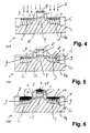
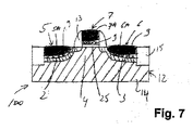
- Figs. 4 to 7 diagrammatically depict a cross section through a semiconductor device in successive stages of the fabrication in accordance with a second embodiment of a method according to the invention.
- Figs. 4 to 7 diagrammatically depict a cross section through a semiconductor device in successive stages of the fabrication in accordance with a second embodiment of a method according to the invention.
- the differences compared to the method described above will be explained.
- Corresponding or identical process steps can be carried out as discussed above in connection with the first exemplary embodiment.
- the first metal just as in the first exemplary embodiment, may be a metal which is inert with respect to silicon, such as for example tungsten, tantalum, niobium or zirconium.
- This ion implantation step automatically provides the desired openings between the atoms of the first metal in the metal cluster layer 9. Moreover, this method is accurate, reproducible and easy to carry out locally.
- the implantation energy may, for example, be 40 keV, and the implantation dose may, for example, be 1 to 5 ⁇ 10 15 at/cm 2 .
- a metal region 8, formed from a second metal is provided (cf. Fig. 5).
- metal silicides 5A, 6A, 7A can be formed at the location of the source and drain regions 2, 3 and at the location of the gate electrode 1, with the clusters being displaced downwards from metal cluster layer 9 by the Kirkendall effect (cf. Figure 6).
- a second heat treatment which can be carried out at a temperature of between 600°C and 850°C, these processes are continued until, for example, the silicon has been completely consumed at the location of the gate electrode 1 (cf. Fig. 7).
- the further processing of the semiconductor device can then be carried out in the customary way which is known to the person skilled in the art.
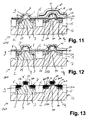
- Figs. 8 to 13 diagrammatically depict a cross section through a semiconductor device in successive stages of the fabrication in accordance with a third embodiment of a method according to the invention.
- the most significant difference between this exemplary embodiment and the first exemplary embodiment resides in the fact that in the present exemplary embodiment a CMOS IC is fabricated, in which, therefore, both NMOS and PMOS transistors are formed.
- the semiconductor body 1 comprises two channel regions 4, 40 of opposite conduction types, it being possible for the channel region 4 to be formed by, for example, a suitable ion implantation into the substrate 14.
- one of the transistors in the present exemplary embodiment the first transistor, is covered with a mask 26, which may be formed, for example, from silicon dioxide (Fig. 8).
- a metal cluster layer 90 in this exemplary embodiment formed from metal clusters of a first metal which is inert with respect to silicon, such as for example tungsten, tantalum, zirconium or niobium, is formed on the surface of the semiconductor body 12 (cf. Fig. 9).
- a second metal layer 80 is applied, formed from a second metal which has siliciding properties.
- the applied layers 80, 90 are removed again at the location of the first transistor with the aid of, for example, a lift-off process which also removes the mask 26.
- the second transistor, and therefore also metal cluster layer 90 and metal layer 80, is covered with a mask 27 (Fig. 10).
- a metal cluster layer 9, formed from a third metal which is inert for reaction with silicon and is preferably a different metal from the first metal which was selected for the metal cluster layer 90 of the second transistor, and a metal layer 8, formed from a fourth metal having siliciding properties, are applied (Fig. 11).
- these layers 8, 9 are removed at the location of the second transistor, for example by a lift-off process, with mask 27 also being removed.
- metal silicides 5A, 6A, 7A and in this case also metal silicides 50A, 60A and 70A, which preferably contain a different metal from metal silicides 5A, 6A, 7A, are formed at the location of the first transistor and the second transistor, respectively, once again in one or more heat treatments.
- metal cluster layers 9, 90 are formed beneath the metal silicides 5A, 6A, 7A and 50A, 60A, 70A which have been formed and in the vicinity of the dielectric region 25 and 250.
- the metal cluster layer 9 for this transistor is selected to be a metal whose work function is closest to the value of approximately 4.2 eV desired for such a transistor. If the second transistor is then a PMOST, the metal cluster layer 90 for this transistor is selected to be a different metal, the work function of which is closer to the value of approximately 5.2 eV which is desired for such a transistor.
- this variant can easily be modified, for example to give a variant in which the metal 8 at the two transistors is the same and has the same thickness. In that case, the lift-off of the masks 26 and 27 is carried out, for example, before the metal region 8 is formed. It is also possible, by means of a simple variant, if desired for the source and drain regions 2, 3 and 20, 30 of both the NMOST and the PMOST to be provided with a metal cluster layer 9, 90 made from the same metal.
- the material of which the control electrode 1 is made there are three important materials, i.e. the material of which the control electrode 1 is made, the material of the metal layer 8 and the material of the metalclusterlayer 9.
- the material of the control electrode 1 en the material of the metal layer 8 have to form a junction in which only one diffusing material is present.
- the material of which the control electrode 1 is formed has thereby to be chosen such that it comprises the diffusing element, because then, according to the invention, the atoms of the cluster layer 9 are pushed in the direction of the dielectric region 25.
- the material of which the control electrode 1 is formed cannot have a negative influence on the dielectric region 25.
- the most important requirement for the method according to the present invention is that the material from which the metalclusterlayer 9 is made has to behave as a so-called "Kirkendall marker". This means that the material has to be inert and substantially immovable during the formation of the silicide compound. With substantially immovable is meant that the material may not diffuse at relevant temperatures at which the silicide compound is formed.
- the invention is not restricted to the exemplary embodiments described, since numerous variations and modifications are possible for the person skilled in the art within the scope of the invention. For example, it is possible to fabricate devices having a different geometry and/or different dimensions.
- a substrate 14 made from Si it is also possible to use a substrate 14 made from glass, ceramic or a plastic.
- the semiconductor body 12 can then be formed by the so-called SOI (silicon on insulator). In this context, it is optionally possible to use a so-called substrate transfer technique.
- the dielectric layer 25 it is not necessary for the dielectric layer 25 to be of the same material or the same thickness for all the transistors.
- the device 100 may comprise further active and passive semiconductor elements or electronic components, such as a greater number of diodes and/or transistors and resistors and/or capacitors, optionally in the form of an integrated circuit.
- the fabrication is obviously adapted appropriately.
- the method can advantageously also be used for the fabrication of individual (semi-)discrete devices which comprise one, optionally bipolar, transistor or even one diode.
Landscapes
- Electrodes Of Semiconductors (AREA)
- Insulated Gate Type Field-Effect Transistor (AREA)
- Metal-Oxide And Bipolar Metal-Oxide Semiconductor Integrated Circuits (AREA)
- Thin Film Transistor (AREA)
- Internal Circuitry In Semiconductor Integrated Circuit Devices (AREA)
Applications Claiming Priority (2)
| Application Number | Priority Date | Filing Date | Title |
|---|---|---|---|
| BE200300546 | 2003-10-17 | ||
| BE2003/0546A BE1015721A3 (nl) | 2003-10-17 | 2003-10-17 | Werkwijze voor het reduceren van de contactweerstand van de aansluitgebieden van een halfgeleiderinrichting. |
Publications (1)
| Publication Number | Publication Date |
|---|---|
| EP1524686A1 true EP1524686A1 (de) | 2005-04-20 |
Family
ID=34318707
Family Applications (1)
| Application Number | Title | Priority Date | Filing Date |
|---|---|---|---|
| EP04077815A Withdrawn EP1524686A1 (de) | 2003-10-17 | 2004-10-13 | Verfahren zur Reduzierung des Kontaktwiderstandes von Anschlussbereichen in einem Halbleiterbauelement |
Country Status (6)
| Country | Link |
|---|---|
| US (2) | US7189648B2 (de) |
| EP (1) | EP1524686A1 (de) |
| JP (1) | JP4722448B2 (de) |
| CN (1) | CN100437943C (de) |
| BE (1) | BE1015721A3 (de) |
| TW (1) | TWI248651B (de) |
Cited By (3)
| Publication number | Priority date | Publication date | Assignee | Title |
|---|---|---|---|---|
| WO2007105157A3 (en) * | 2006-03-14 | 2007-11-15 | Nxp Bv | Source and drain formation |
| EP1928021A1 (de) * | 2006-11-29 | 2008-06-04 | Interuniversitair Microelektronica Centrum (IMEC) | Herstellungsverfahren einer Halbleitervorrichtung mit vollständigem Dual-Silizidgate |
| WO2009133509A1 (en) * | 2008-04-29 | 2009-11-05 | Nxp B.V. | Integrated circuit manufacturing method and integrated circuit |
Families Citing this family (28)
| Publication number | Priority date | Publication date | Assignee | Title |
|---|---|---|---|---|
| US7405112B2 (en) * | 2000-08-25 | 2008-07-29 | Advanced Micro Devices, Inc. | Low contact resistance CMOS circuits and methods for their fabrication |
| JP4011024B2 (ja) | 2004-01-30 | 2007-11-21 | 株式会社ルネサステクノロジ | 半導体装置およびその製造方法 |
| US7101744B1 (en) * | 2005-03-01 | 2006-09-05 | International Business Machines Corporation | Method for forming self-aligned, dual silicon nitride liner for CMOS devices |
| US7939440B2 (en) * | 2005-06-15 | 2011-05-10 | Spansion Llc | Junction leakage suppression in memory devices |
| JP4981307B2 (ja) * | 2005-11-18 | 2012-07-18 | シャープ株式会社 | 電子装置、電子回路及び電子機器 |
| US20070131985A1 (en) * | 2005-11-29 | 2007-06-14 | Kazunori Fujita | Semiconductor device and method for manufacturing the same |
| US7659580B2 (en) * | 2005-12-02 | 2010-02-09 | Semiconductor Energy Laboratory Co., Ltd. | Semiconductor device and manufacturing method thereof |
| JP4864498B2 (ja) * | 2006-03-15 | 2012-02-01 | 株式会社東芝 | 半導体装置およびその製造方法 |
| US8362567B2 (en) * | 2006-07-13 | 2013-01-29 | National University Corporation Tohoku University | Semiconductor device |
| JP4247257B2 (ja) | 2006-08-29 | 2009-04-02 | 株式会社東芝 | 半導体装置の製造方法 |
| JP2008078403A (ja) * | 2006-09-21 | 2008-04-03 | Matsushita Electric Ind Co Ltd | 半導体装置及びその製造方法 |
| US7812414B2 (en) * | 2007-01-23 | 2010-10-12 | Taiwan Semiconductor Manufacturing Company, Ltd. | Hybrid process for forming metal gates |
| US7754554B2 (en) * | 2007-01-31 | 2010-07-13 | Globalfoundries Inc. | Methods for fabricating low contact resistance CMOS circuits |
| US20080191285A1 (en) * | 2007-02-09 | 2008-08-14 | Chih-Hsin Ko | CMOS devices with schottky source and drain regions |
| JP4960125B2 (ja) | 2007-03-22 | 2012-06-27 | 株式会社東芝 | 半導体装置およびその製造方法 |
| US20090134469A1 (en) * | 2007-11-28 | 2009-05-28 | Interuniversitair Microelektronica Centrum (Imec) Vzw | Method of manufacturing a semiconductor device with dual fully silicided gate |
| JP5221112B2 (ja) | 2007-11-29 | 2013-06-26 | 株式会社東芝 | 半導体装置の製造方法および半導体装置 |
| KR20090074561A (ko) * | 2008-01-02 | 2009-07-07 | 주식회사 하이닉스반도체 | 반도체소자의 컨택 형성방법 |
| US8536660B2 (en) * | 2008-03-12 | 2013-09-17 | Taiwan Semiconductor Manufacturing Company, Ltd. | Hybrid process for forming metal gates of MOS devices |
| US20100052077A1 (en) * | 2008-08-27 | 2010-03-04 | Taiwan Semiconductor Manufacturing Company, Ltd. | High-k metal gate structure including buffer layer |
| JP5611574B2 (ja) * | 2009-11-30 | 2014-10-22 | 株式会社東芝 | 抵抗変化メモリ及びその製造方法 |
| JP5538975B2 (ja) * | 2010-03-29 | 2014-07-02 | ルネサスエレクトロニクス株式会社 | 半導体装置の製造方法 |
| CN102214687A (zh) * | 2010-04-07 | 2011-10-12 | 中国科学院微电子研究所 | 一种栅堆叠结构、半导体器件及二者的制造方法 |
| CN103137486B (zh) * | 2011-11-30 | 2016-08-03 | 中国科学院微电子研究所 | 半导体器件制造方法 |
| US9059096B2 (en) | 2012-01-23 | 2015-06-16 | International Business Machines Corporation | Method to form silicide contact in trenches |
| US20130241007A1 (en) | 2012-03-15 | 2013-09-19 | International Business Machines Corporation | Use of band edge gate metals as source drain contacts |
| US9177810B2 (en) | 2014-01-29 | 2015-11-03 | International Business Machines Corporation | Dual silicide regions and method for forming the same |
| CN110931361B (zh) * | 2019-11-28 | 2023-03-14 | 中国科学院微电子研究所 | 一种mos器件、制造方法、集成电路及电子设备 |
Citations (8)
| Publication number | Priority date | Publication date | Assignee | Title |
|---|---|---|---|---|
| EP0651076A1 (de) * | 1993-10-29 | 1995-05-03 | International Business Machines Corporation | Verfahren zur Senkung der Phasenübergangstemperatur eines Metallsilizids |
| US6177319B1 (en) * | 1999-01-16 | 2001-01-23 | United Microelectronics Corp. | Method of manufacturing salicide layer |
| US6211000B1 (en) * | 1999-01-04 | 2001-04-03 | Advanced Micro Devices | Method of making high performance mosfets having high conductivity gate conductors |
| US6281556B1 (en) * | 1998-03-13 | 2001-08-28 | Stmicroelectronics S.A. | Process for forming a low resistivity titanium silicide layer on a silicon semiconductor substrate and the resulting device |
| US20020011636A1 (en) * | 2000-07-21 | 2002-01-31 | Mitsubishi Denki Kabushiki Kaisha | Semiconductor device, manufacturing method thereof, and CMOS transistor |
| US6372566B1 (en) * | 1997-07-03 | 2002-04-16 | Texas Instruments Incorporated | Method of forming a silicide layer using metallic impurities and pre-amorphization |
| US6440806B1 (en) * | 2001-04-30 | 2002-08-27 | Advanced Micro Devices, Inc. | Method for producing metal-semiconductor compound regions on semiconductor devices |
| WO2003075330A1 (en) * | 2002-02-28 | 2003-09-12 | Advanced Micro Devices, Inc. | Method of forming different silicide portions on different silicon-containing regions in a semiconductor device |
Family Cites Families (9)
| Publication number | Priority date | Publication date | Assignee | Title |
|---|---|---|---|---|
| JPS618916A (ja) * | 1984-06-21 | 1986-01-16 | インタ−ナシヨナル・ビジネス・マシ−ンズ・コ−ポレ−シヨン | ド−プ領域の形成方法 |
| KR100197996B1 (ko) * | 1996-06-29 | 1999-06-15 | 김영환 | 반도체 소자의 제조방법 |
| JPH1098012A (ja) * | 1996-09-20 | 1998-04-14 | Sony Corp | 半導体装置の製造方法 |
| US5851891A (en) * | 1997-04-21 | 1998-12-22 | Advanced Micro Devices, Inc. | IGFET method of forming with silicide contact on ultra-thin gate |
| JP2001320045A (ja) * | 2000-05-11 | 2001-11-16 | Nec Corp | Mis型半導体装置の製造方法 |
| US6873051B1 (en) * | 2002-05-31 | 2005-03-29 | Advanced Micro Devices, Inc. | Nickel silicide with reduced interface roughness |
| DE10334353A1 (de) * | 2003-07-25 | 2005-02-17 | Forschungszentrum Jülich GmbH | Verfahren zur Herstellung eines Kontaktes und elektronisches Bauelement, umfassend derartige Kontakte |
| DE10335101B4 (de) * | 2003-07-31 | 2010-02-04 | Advanced Micro Devices, Inc., Sunnyvale | Verfahren zur Herstellung einer Polysiliziumleitung mit einem Metallsilizidgebiet, das eine Linienbreitenreduzierung ermöglicht |
| US6936508B2 (en) * | 2003-09-12 | 2005-08-30 | Texas Instruments Incorporated | Metal gate MOS transistors and methods for making the same |
-
2003
- 2003-10-17 BE BE2003/0546A patent/BE1015721A3/nl not_active IP Right Cessation
-
2004
- 2004-10-13 EP EP04077815A patent/EP1524686A1/de not_active Withdrawn
- 2004-10-14 TW TW093131117A patent/TWI248651B/zh not_active IP Right Cessation
- 2004-10-15 JP JP2004301664A patent/JP4722448B2/ja not_active Expired - Lifetime
- 2004-10-15 US US10/966,141 patent/US7189648B2/en not_active Expired - Lifetime
- 2004-10-18 CN CNB2004100981418A patent/CN100437943C/zh not_active Expired - Lifetime
-
2006
- 2006-09-22 US US11/526,116 patent/US7320939B2/en not_active Expired - Lifetime
Patent Citations (8)
| Publication number | Priority date | Publication date | Assignee | Title |
|---|---|---|---|---|
| EP0651076A1 (de) * | 1993-10-29 | 1995-05-03 | International Business Machines Corporation | Verfahren zur Senkung der Phasenübergangstemperatur eines Metallsilizids |
| US6372566B1 (en) * | 1997-07-03 | 2002-04-16 | Texas Instruments Incorporated | Method of forming a silicide layer using metallic impurities and pre-amorphization |
| US6281556B1 (en) * | 1998-03-13 | 2001-08-28 | Stmicroelectronics S.A. | Process for forming a low resistivity titanium silicide layer on a silicon semiconductor substrate and the resulting device |
| US6211000B1 (en) * | 1999-01-04 | 2001-04-03 | Advanced Micro Devices | Method of making high performance mosfets having high conductivity gate conductors |
| US6177319B1 (en) * | 1999-01-16 | 2001-01-23 | United Microelectronics Corp. | Method of manufacturing salicide layer |
| US20020011636A1 (en) * | 2000-07-21 | 2002-01-31 | Mitsubishi Denki Kabushiki Kaisha | Semiconductor device, manufacturing method thereof, and CMOS transistor |
| US6440806B1 (en) * | 2001-04-30 | 2002-08-27 | Advanced Micro Devices, Inc. | Method for producing metal-semiconductor compound regions on semiconductor devices |
| WO2003075330A1 (en) * | 2002-02-28 | 2003-09-12 | Advanced Micro Devices, Inc. | Method of forming different silicide portions on different silicon-containing regions in a semiconductor device |
Non-Patent Citations (2)
| Title |
|---|
| CABRAL C ET AL: "Lowering the formation temperature of the C54-TiSi/sub 2/ phase using a metallic interfacial layer", J. MATER. RES. (USA), JOURNAL OF MATERIALS RESEARCH, FEB. 1997, MATER. RES. SOC, USA, vol. 12, no. 2, February 1997 (1997-02-01), pages 304 - 307, XP008032437, ISSN: 0884-2914 * |
| MASZARA W P ET AL: "Transistors with dual work function metal gates by single full silicidation (FUSI) of polysilicon gates", INTERNATIONAL ELECTRON DEVICES MEETING 2002. IEDM. TECHNICAL DIGEST. SAN FRANCISCO, CA, DEC. 8 - 11, 2002, NEW YORK, NY : IEEE, US, 8 December 2002 (2002-12-08), pages 367 - 370, XP010626061, ISBN: 0-7803-7462-2 * |
Cited By (3)
| Publication number | Priority date | Publication date | Assignee | Title |
|---|---|---|---|---|
| WO2007105157A3 (en) * | 2006-03-14 | 2007-11-15 | Nxp Bv | Source and drain formation |
| EP1928021A1 (de) * | 2006-11-29 | 2008-06-04 | Interuniversitair Microelektronica Centrum (IMEC) | Herstellungsverfahren einer Halbleitervorrichtung mit vollständigem Dual-Silizidgate |
| WO2009133509A1 (en) * | 2008-04-29 | 2009-11-05 | Nxp B.V. | Integrated circuit manufacturing method and integrated circuit |
Also Published As
| Publication number | Publication date |
|---|---|
| US20070020930A1 (en) | 2007-01-25 |
| JP2005123626A (ja) | 2005-05-12 |
| US20050112875A1 (en) | 2005-05-26 |
| JP4722448B2 (ja) | 2011-07-13 |
| TWI248651B (en) | 2006-02-01 |
| CN1667808A (zh) | 2005-09-14 |
| US7320939B2 (en) | 2008-01-22 |
| BE1015721A3 (nl) | 2005-07-05 |
| TW200518234A (en) | 2005-06-01 |
| US7189648B2 (en) | 2007-03-13 |
| CN100437943C (zh) | 2008-11-26 |
Similar Documents
| Publication | Publication Date | Title |
|---|---|---|
| US7189648B2 (en) | Method for reducing the contact resistance of the connection regions of a semiconductor device | |
| US6777761B2 (en) | Semiconductor chip using both polysilicon and metal gate devices | |
| EP1524688B1 (de) | Herstellungsverfahren für Halbleiterbauelemente mit silizidierten Elektroden | |
| US20030001219A1 (en) | Novel transistor structure and method of fabrication | |
| EP0689237A1 (de) | Methode zur Bildung von Metallsilizidschichten auf Source- und Draingebiete | |
| US6096591A (en) | Method of making an IGFET and a protected resistor with reduced processing steps | |
| TW200417015A (en) | MOSFET threshold voltage tuning with metal gate stack control | |
| US7338865B2 (en) | Method for manufacturing dual work function gate electrodes through local thickness-limited silicidation | |
| CN100442462C (zh) | Mosfet器件及其制造方法 | |
| US6368960B1 (en) | Double sidewall raised silicided source/drain CMOS transistor | |
| EP1782466A2 (de) | Doppel-gate-cmos-herstellung | |
| KR100499755B1 (ko) | Mdd 와 선택적 cvd 실리사이드를 갖는 디프서브미크론 cmos 소스/드레인 제조방법 | |
| JPH1140679A (ja) | 半導体装置およびその製造方法 | |
| JP2004111549A (ja) | 半導体装置の製造方法 | |
| WO2000036634A2 (en) | Amorphization of substrate to prevent silicide encroachment into channel region of field effect transistor | |
| JPH1131665A (ja) | 半導体集積回路装置の製造方法 | |
| EP1678750A1 (de) | Halbleiterbauelement und verfahren zur herstellung eines solchen halbleiterbauelements | |
| JP2886174B2 (ja) | 半導体装置の製造方法 | |
| US7531459B2 (en) | Methods of forming self-aligned silicide layers using multiple thermal processes | |
| JPH06177067A (ja) | 半導体集積回路装置の製造方法 | |
| KR101012241B1 (ko) | 반도체 소자의 실리사이드 형성 방법 | |
| WO2006003579A1 (en) | Field effect transistor method and device | |
| JP2010192735A (ja) | 半導体素子及びその製造方法 | |
| JPH10294458A (ja) | 半導体装置の製造方法 | |
| JPH1197554A (ja) | 半導体装置およびその製造方法 |
Legal Events
| Date | Code | Title | Description |
|---|---|---|---|
| PUAI | Public reference made under article 153(3) epc to a published international application that has entered the european phase |
Free format text: ORIGINAL CODE: 0009012 |
|
| AK | Designated contracting states |
Kind code of ref document: A1 Designated state(s): AT BE BG CH CY CZ DE DK EE ES FI FR GB GR HU IE IT LI LU MC NL PL PT RO SE SI SK TR |
|
| AX | Request for extension of the european patent |
Extension state: AL HR LT LV MK |
|
| 17P | Request for examination filed |
Effective date: 20050923 |
|
| AKX | Designation fees paid |
Designated state(s): AT BE BG CH CY CZ DE DK EE ES FI FR GB GR HU IE IT LI LU MC NL PL PT RO SE SI SK TR |
|
| 17Q | First examination report despatched |
Effective date: 20081120 |
|
| RAP1 | Party data changed (applicant data changed or rights of an application transferred) |
Owner name: NXP B.V. Owner name: INTERUNIVERSITAIR MICROELEKTRONICA CENTRUM ( IMEC) |
|
| RAP1 | Party data changed (applicant data changed or rights of an application transferred) |
Owner name: NXP B.V. Owner name: IMEC |
|
| STAA | Information on the status of an ep patent application or granted ep patent |
Free format text: STATUS: THE APPLICATION IS DEEMED TO BE WITHDRAWN |
|
| 18D | Application deemed to be withdrawn |
Effective date: 20111111 |