EP1521069A2 - Colorimètre pour la mesure des vraies couleurs - Google Patents
Colorimètre pour la mesure des vraies couleurs Download PDFInfo
- Publication number
- EP1521069A2 EP1521069A2 EP04023051A EP04023051A EP1521069A2 EP 1521069 A2 EP1521069 A2 EP 1521069A2 EP 04023051 A EP04023051 A EP 04023051A EP 04023051 A EP04023051 A EP 04023051A EP 1521069 A2 EP1521069 A2 EP 1521069A2
- Authority
- EP
- European Patent Office
- Prior art keywords
- color
- spectral
- photosensor
- sensor chip
- filter
- Prior art date
- Legal status (The legal status is an assumption and is not a legal conclusion. Google has not performed a legal analysis and makes no representation as to the accuracy of the status listed.)
- Granted
Links
Images


Classifications
-
- G—PHYSICS
- G01—MEASURING; TESTING
- G01J—MEASUREMENT OF INTENSITY, VELOCITY, SPECTRAL CONTENT, POLARISATION, PHASE OR PULSE CHARACTERISTICS OF INFRARED, VISIBLE OR ULTRAVIOLET LIGHT; COLORIMETRY; RADIATION PYROMETRY
- G01J3/00—Spectrometry; Spectrophotometry; Monochromators; Measuring colours
- G01J3/46—Measurement of colour; Colour measuring devices, e.g. colorimeters
- G01J3/50—Measurement of colour; Colour measuring devices, e.g. colorimeters using electric radiation detectors
- G01J3/51—Measurement of colour; Colour measuring devices, e.g. colorimeters using electric radiation detectors using colour filters
- G01J3/513—Measurement of colour; Colour measuring devices, e.g. colorimeters using electric radiation detectors using colour filters having fixed filter-detector pairs
-
- G—PHYSICS
- G01—MEASURING; TESTING
- G01J—MEASUREMENT OF INTENSITY, VELOCITY, SPECTRAL CONTENT, POLARISATION, PHASE OR PULSE CHARACTERISTICS OF INFRARED, VISIBLE OR ULTRAVIOLET LIGHT; COLORIMETRY; RADIATION PYROMETRY
- G01J3/00—Spectrometry; Spectrophotometry; Monochromators; Measuring colours
- G01J3/02—Details
- G01J3/0256—Compact construction
-
- G—PHYSICS
- G01—MEASURING; TESTING
- G01J—MEASUREMENT OF INTENSITY, VELOCITY, SPECTRAL CONTENT, POLARISATION, PHASE OR PULSE CHARACTERISTICS OF INFRARED, VISIBLE OR ULTRAVIOLET LIGHT; COLORIMETRY; RADIATION PYROMETRY
- G01J3/00—Spectrometry; Spectrophotometry; Monochromators; Measuring colours
- G01J3/02—Details
- G01J3/0291—Housings; Spectrometer accessories; Spatial arrangement of elements, e.g. folded path arrangements
-
- G—PHYSICS
- G01—MEASURING; TESTING
- G01J—MEASUREMENT OF INTENSITY, VELOCITY, SPECTRAL CONTENT, POLARISATION, PHASE OR PULSE CHARACTERISTICS OF INFRARED, VISIBLE OR ULTRAVIOLET LIGHT; COLORIMETRY; RADIATION PYROMETRY
- G01J3/00—Spectrometry; Spectrophotometry; Monochromators; Measuring colours
- G01J3/46—Measurement of colour; Colour measuring devices, e.g. colorimeters
- G01J3/465—Measurement of colour; Colour measuring devices, e.g. colorimeters taking into account the colour perception of the eye; using tristimulus detection
Definitions
- the invention relates to a photosensor for color measurement based on three Spectral components, for detecting the sensor chip by an upstream Interference filter structure has three different sensitive faces, wherein the subareas provide measurements that are in a suitable color space in Color values are implemented, especially for the high-precision color measurement (Point measurement) when testing and ensuring the color consistency of technical Surfaces and any consumer goods.
- the basic principle of a spectrally adjusted semiconductor sensor is already known from US 3,996,461.
- a thin film optical filter based on an interference multilayer system is described for a silicon photosensor, in order to limit the sensitivity of the sensor to the spectral sensitivity of the human eye.
- the high refractive index layers are made of titanium oxide and the low refractive index silicon oxide.
- the resulting filter system corresponds to a Y characteristic of the spectral sensitivity curve of the human eye, without allowing a spectrally selective resolution of the color spectrum in terms of the assignment of color values or standard spectral colors, since the filter layers are not structured, but are applied to several sensor elements at the same time.
- US 5,246,803 discloses structured dichroic filters for solid state electronic image sensors which are made by alternately depositing on the sensor surface or a glass layer. Here, the varying deposition of SiO 2 and TiO 2 layers under vacuum conditions and low temperature for the production of color filters was described, the spectral characteristic of the filter controlled by the number and thickness of the layers and the formation and deposition of the layers is repeated as often to create red, green and blue filters. According to US Pat. No.
- the invention is based on the object, a new way of color measurement on the basis of a tristimulus method with three, different by upstream to find spectrally selective interference filters generated colorimetric measurements using simple means an almost standard true color measurement without consuming Reference light calibration allowed.
- the task is in a photosensor for color measurement Basis of three spectral components, for their detection a sensor chip at least three different sensitivity through an upstream interference filter structure Partial surfaces, wherein the interference filter structure three different Alternating layer systems of silicon dioxide and titanium dioxide for selective Transmitting incident light in the different sub-areas of the sensor chip contains and the subareas provide readings, solved by the Photosensor three with different on the spectral characteristics of the human eye adapted interference filters covered partial surfaces, the each circular-sector-shaped distributed around a central point with intermediate passive webs are arranged, and that each interference filter is one in his Transmission characteristic over the wavelength of the spectrally measured light the sensitivity of the human eye is adjusted so that the product from basic sensitivity of the partial surfaces of the photosensor and transmission of the Interference filter proportional to the normal spectral value of the human Eye is for the relevant coordinate of the color space, so the transmitted spectral components in the sub-areas produce measured values that at simple scaling to each other in the color space in spectral color values can
- the transmission characteristic of each interference filter is advantageously prepared with a tolerance of the layer thicknesses of less than 2%. Since adherence to significantly lower layer thickness tolerances (for example ⁇ 1%) is currently unrealistic from a technological point of view, a linear correction of the measured values output by the partial surfaces is undertaken to compensate for the production-related layer thickness deviations, as far as the accuracy of the color measurement requires for the desired application.
- this can be done by global matrixing for correcting the output measured values for the entire color space and, on the other hand, with increased accuracy requirements, eg for output of accurate colorimetric values, by linear correction of the output measured values by means of local matrixing of suitable tetrahedron regions of the color space.
- the interference filter are applied directly to the semiconductor diodes of the sensor chip.
- the interference filters are preferably applied directly to silicon diodes of the sensor chip.
- the Si diodes are best produced in a specially adapted for the visual spectral range PIN diode technology to already achieve an advantageous basic sensitivity of the Si diodes of the entire sensor chip.
- there is the particular additional advantage that the aging and temperature dependence of the entire system of photodiode and interference filter are negligible.
- the interference filters can also be suitably applied to Si diodes which have been produced in a CMOS technology adapted to the visual spectral range.
- the interference filters can also be applied to a sensor chip with germanium diodes or with diodes based on InGaAs.
- the interference filters can also be advantageously applied over the Si diodes (partial surfaces) of the sensor chip on a separate glass plate or by using lift-off techniques become.
- the differently sensitive partial surfaces on the sensor chip are preferably formed as a circle segment (circular area third) due to applied interference filters and arranged uniformly distributed about a central point.
- a scaling of the spectral characteristics of the partial surfaces of the photosensor to the sensitivity distribution of the eye is at least partially realizable hardware, is that the covered with the matched interference filters, different sensitive sub-areas on the sensor chip as a circular area sectors of different surface area around a central point are arranged, wherein the different surface areas are tuned to that a lower base sensitivity of a partial surface, which comes about due to limited wavelength transmission of the associated interference filter, is compensated by a correspondingly larger surface area of the partial surface of the photosensor.
- the partial surfaces coated with different interference filters are distributed uniformly around a central point in the form of rhombi with a 120 ° angle, so that they form a regular hexagon as a triple color segment.
- these hexagonal triple color segments can be arranged on the sensor chip so as to form a honeycomb structure around a plurality of central points with the same webs and uniformly distributed, with subareas of the same spectral sensitivity having no adjacent side edges with one another.
- the photosensor according to the invention it is possible to color measurements based a tristimulus method with three, by different spectrally selective Interference filter to produce generated color readings, by means of the Standard spectral function of the human eye adapted interference filter Near-standard true color measurement without complex reference light calibration allowed. As a result, color differences in with the human eye of comparable quality are separated. Furthermore, the measured Photocurrents of the three subareas of the sensor for certain accuracy classes of the Color measurement directly convertible into standardized color spaces. Leave with the invention Realize inexpensive color sensors and in powerful compact Integrate colorimeters.
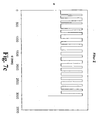
- the color sensor according to the invention consists in its basic structure - as shown schematically in FIG. 1 - of a sensor chip 1 with photosensitive subareas 11, and an interference filter structure 2 with spectrally differently sensitive interference filters 21, 22, and 23 (only in FIGS. 5 and 6).
- the interference filter system 2 has in each case as triple element three differently dimensioned alternating layer systems of silicon dioxide and titanium dioxide layers whose spectral transmission is adapted to the standard spectral functions of the human eye.
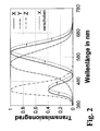
- FIG. 2 shows the normalized standard spectral functions of the interference filters 21, 22 and 23 for the respective coordinate of the selected CIE color space.
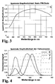
- the spectral transmission of the interference filters 21, 22 and 23 is so dimensioned that the product of basic sensitivity S (shown in FIG. 3 for Si diodes according to PIN technology) and transmission characteristic of the respective interference filter 21, 22 or 23 is proportional to the desired normal spectral value curve ,
- the product of basic sensitivity S and filter transmission X, Y, Z is always used as the overall spectral sensitivity of the color sensor, as shown in FIG. 4 for a specific case (based on FIG. 3).
- the base material of the sensor chip 1 is equipped with Si diodes, which were manufactured in a specially adapted for the visual spectral range PIN diode technology and thus in their spectral sensitivity of the human eye are best approximated.
- the sensitivity curve of a PIN diode produced in this way is shown in FIG. 3.
- Ge or InGaAs diodes can also be used instead of Si diodes.
- FIG. 4 illustrates the overall spectral sensitivity distribution of the color sensor when the interference filter structure 2 with its three different interference filters 21, 22 and 23 for the X, Y and Z components on a sensor chip 1 according to the sensitivity function of FIG. 3 (eg In order to obtain the resulting transmission characteristics of the color sensor in the three coordinates of the color space shown in Figure 4, the interference filters 21, 22 and 23 are suitable to vary with respect to the layer thicknesses of the alternating layers Associated system of interference filters 21, 22, 23 is indicated for example in Fig. 7a (X-filter), 7b (Y-filter) and Fig. 7c (Z-filter) for the coordinates of the color space.
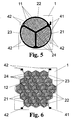
- FIG. 5 shows a variant of the sensor chip 1 for a selectively measurable color sensor.
- the black area is the cathode 41 of the complete triple element of the color sensor.
- the white areas represent the anodes 42 of the three partial areas 11 of the photosensor, from which the occurring photocurrents are derived as measured values.
- Striped subarea 11 is intended, in the selected case, to have the X-transmission function (as shown in FIG. 2) generated by interference filter 21, while checkered and brick-patterned subarea 11 show the Y and Z transmission functions of interference filters 22 and 23, respectively (as shown in FIG 2) symbolize.
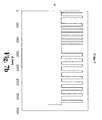
- FIG. 6 A special design of the color sensor according to the invention for planar Color measurements are shown in Fig. 6 in a plan view of the sensor chip 1.
- the sensor chip 1 has a plurality of honeycomb-shaped triple elements 12, each of which three Si diodes with the different interference filters 21, 22 and 23 exist.
- the triple elements 12 are arranged to each other so that an interference filter 21, 22 or 23 no common edge with the same interference filter 21, 22 or 23 has each of the adjacent triple elements 12. This results in a regular structure on the entire sensor chip 1, which is capable of one Measuring the uniformity of a color impression of a surface.
- the sequence of alternating layers of the X-filter of the X-filter of the color sensor (partial surface 11 for the spectral function of the red sensitivity of the human eye is particularly variable with respect to the layer thicknesses.) This is due to the likewise complicated course
- the spectral transmission function approximated according to the solid line for the X coordinate of the color space in Fig. 2.
- the interference filter 22 indicated in Fig. 7b is designed as a switching system for the Y filter of the color sensor
- the interference filter 23 for the blue "color perception of the color sensor" approximated by the Z filter shown in Fig.
- the layer thickness d of the individual interference filters 21, 22 and 23 was set at less than 4 ⁇ m and preferably set at 3000 nm ⁇ d ⁇ 3500 nm.
- the interference filters 21, 22 and 23 computed by computer-aided optimization (the required to approximate the standard spectral function of the eye transmission functions) have between 30 and 40 layers. In the example shown in FIGS.
- the X-filter 35, the Y-filter 37 and the Z-filter 34 comprise alternating layers of TiO 2 and SiO 2 .
- the interference filters 21, 22 and 23 thus calculated can be applied directly to the Si diodes of the sensor chip 1 by plasma-assisted coating (after application of a passivation layer). On the other hand, they can also be applied to a glass substrate or manufactured with lift-off techniques and subsequently adjusted over the silicon chip in order to avoid wasting valuable semiconductor material if layer tolerances are not met for the complicated interference filter structure 2.
- Luminous Color stimuli are therefore advantageous to reinterpret as body color by e.g. whose emission spectrum scales to values ⁇ 1 and thus as a transmission spectrum an equivalent filter.
- Scaling i. an alignment of the sensor channels to each other (i.e., a white balance the signals / measured values of the sub-areas 11 of the three-channel photosensor to the standard spectral functions of the human eye) is self-evident essential. Apart from this scaling should under normal conditions no correction the measured values are required.
- a narrowband color stimulus can be simulated as a bandpass spectral interference filter, with a typical measure of the spectral bandwidth of a conventional 15 nm interference filter can be assumed.
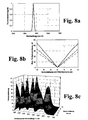
- Fig. 8a shows the spectral transmission (or remission) of such an object for a centroid wavelength of 555 nm.
- the transmittance is set at 15 nm spectral width and a 1 / e drop and examined with variable centroid wavelength.
- the filter curve is shifted from -12 nm to +12 nm in 0.5 nm steps for error estimation and determined for each shift ⁇ E of the emission spectrum of target color and measured color in CIELAB space, depending on from the centroid wavelength of the target transmission.
- the maximum value of ⁇ E over all centroid wavelengths was plotted as a function of the filter curve displacement in FIG. 8b.
- the overall result of the error calculation is illustrated in Figure 8c as a function of the centroid wavelength and the shift of the filter function of the model target in the CIELAB space in the event that only the X filter function has been shifted.
- the measured color deviation for each centroid wavelength is approximately proportional to the amount of filter curve shift.
- LED's can be set by specifying a transmission filter with a filter width of 40 nm, because the spectral behavior of typical LEDs is good is approximated. It is thus replaced by an object with corresponding Transmission failed.
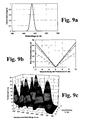
- the transition area of the ramp function is 50 nm Width specified and its center position (hereinafter called ramp position), which is shown in Fig. 10a at 555 nm Fig. 10a, over the entire visible spectrum varied.
- FIG. 11a Another example is a flatter ramp function (low color contrast) examined according to Fig. 11a, again by the ramp position with a Transition range of 50 nm over the entire visible spectrum varies.
- the maximum color deviation ⁇ E in the CIELAB space is thereby characterized in that because of the reduced color saturation according to FIG Significantly reduce sentimental color deviations.
- Fig. 11c shows about the same qualitative behavior as Fig. 10c, but small amounts of error.
- the standard spectral value of x j is multiplicatively composed of the filter transmission T j (setpoint) and the basic sensitivity S of the sensor.
- ⁇ can be represented as the product of the light source spectrum ⁇ B and the spectral reflectance ⁇ .
- the color sensor according to the invention should still be able to achieve a clear leap in quality.
- the local linear correction is still capable of further development and can become even more profound in order to create sensor specifications with peak parameters in a large number of applications.
- the optimization criterion has to be determined carefully according to the measurement tasks to be solved. The results so far, however, already clearly show that a linear approach is sufficient for the single errors as well as the linear superposition. Because of the linearity approach thus established, it is possible to calculate the maximum manufacturing tolerances for the filter systems for approaching the standard spectral function of the human eye from given maximum measurement errors and to set them during production.
Landscapes
- Physics & Mathematics (AREA)
- Spectroscopy & Molecular Physics (AREA)
- General Physics & Mathematics (AREA)
- Spectrometry And Color Measurement (AREA)
Applications Claiming Priority (2)
| Application Number | Priority Date | Filing Date | Title |
|---|---|---|---|
| DE10346595 | 2003-10-02 | ||
| DE10346595 | 2003-10-02 |
Publications (3)
| Publication Number | Publication Date |
|---|---|
| EP1521069A2 true EP1521069A2 (fr) | 2005-04-06 |
| EP1521069A3 EP1521069A3 (fr) | 2007-01-24 |
| EP1521069B1 EP1521069B1 (fr) | 2016-06-29 |
Family
ID=34306310
Family Applications (1)
| Application Number | Title | Priority Date | Filing Date |
|---|---|---|---|
| EP04023051.8A Expired - Lifetime EP1521069B1 (fr) | 2003-10-02 | 2004-09-28 | Colorimètre pour la mesure des vraies couleurs |
Country Status (2)
| Country | Link |
|---|---|
| US (1) | US7132644B2 (fr) |
| EP (1) | EP1521069B1 (fr) |
Cited By (5)
| Publication number | Priority date | Publication date | Assignee | Title |
|---|---|---|---|---|
| EP1857280A2 (fr) | 2006-05-15 | 2007-11-21 | Koenig & Bauer Aktiengesellschaft | Presse rotative dotée d'au moins un système d'encrage et un système de mesure en ligne des couleurs |
| DE102006022530A1 (de) * | 2006-05-15 | 2007-11-22 | Koenig & Bauer Aktiengesellschaft | Rollenrotationsdruckmaschine mit mindestens einem Farbwerk und mit einem Inline-Inspektionssystem |
| WO2008065170A1 (fr) | 2006-11-30 | 2008-06-05 | Osram Opto Semiconductors Gmbh | Détecteur de rayonnement à sensibilité spectrale réglable |
| WO2021185979A1 (fr) * | 2020-03-19 | 2021-09-23 | ams Sensors Germany GmbH | Capteur de couleur multicanal |
| US11199450B2 (en) | 2017-05-16 | 2021-12-14 | Ams Ag | Optical sensor and method for detecting electromagnetic radiation |
Families Citing this family (27)
| Publication number | Priority date | Publication date | Assignee | Title |
|---|---|---|---|---|
| DE10345410A1 (de) * | 2003-09-30 | 2005-05-04 | Osram Opto Semiconductors Gmbh | Strahlungsdetektor |
| CN1938864B (zh) * | 2004-03-31 | 2011-03-23 | 奥斯兰姆奥普托半导体有限责任公司 | 辐射探测器 |
| EP1812782A4 (fr) * | 2004-11-16 | 2010-04-07 | Datacolor Holding Ag | Procede pour concevoir un colorimetre dote de filtres cie de correspondance des couleurs integres |
| EP1812781A4 (fr) * | 2004-11-17 | 2010-04-07 | Datacolor Holding Ag | Colorimetre dote de filtres colorants integraux |
| US20060146330A1 (en) * | 2005-01-04 | 2006-07-06 | Selvan Maniam | Color measurements of ambient light |
| US7580130B2 (en) * | 2005-03-23 | 2009-08-25 | Datacolor Holding Ag | Method for designing a colorimeter having integral illuminant-weighted CIE color-matching filters |
| US7474402B2 (en) * | 2005-03-23 | 2009-01-06 | Datacolor Holding Ag | Reflectance sensor for integral illuminant-weighted CIE color matching filters |
| EP1938063B1 (fr) * | 2005-08-15 | 2011-12-21 | X-Rite Incorporated | Spectrophotometre comprenant un element de guidage de lumiere |
| US8022632B2 (en) * | 2006-01-19 | 2011-09-20 | Koninklijke Philips Electronics N.V. | Color-controlled illumination device |
| US20070194212A1 (en) * | 2006-02-23 | 2007-08-23 | National Taiwan University | Ambient light photodetector |
| US7777915B2 (en) * | 2006-06-15 | 2010-08-17 | Eastman Kodak Company | Image control system and method |
| DE102006028672B3 (de) * | 2006-06-22 | 2007-10-18 | Infineon Technologies Ag | Single-Chip-Einzelhalbleiter-Optobauelement, insbesondere Optotyristor oder Optotriac |
| TW200832687A (en) * | 2007-01-30 | 2008-08-01 | Univ Nat Taiwan | Ambient light sensor |
| US7894064B2 (en) * | 2008-01-10 | 2011-02-22 | Hewlett-Packard Development Company, L.P. | Optical device for dispersing light |
| BRPI0909580B1 (pt) * | 2008-05-28 | 2019-07-02 | Akzo Nobel Coatings International B. V. | Método de determinação de uma variante correspondente de uma cor padrão de uma tinta de reparo que iguale a cor de efeito de um objeto a ser reparado |
| US20100208266A1 (en) * | 2009-02-17 | 2010-08-19 | Colman Shannon | Tristimulus colorimeter having integral dye filters |
| JP2010258110A (ja) * | 2009-04-22 | 2010-11-11 | Panasonic Corp | 固体撮像素子 |
| JP5696843B2 (ja) * | 2011-03-23 | 2015-04-08 | 株式会社リコー | 電子写真用オーバーコート組成物の評価方法、並びに電子写真用オーバーコート組成物、電子写真形成方法、及び電子写真形成装置 |
| KR20140007583A (ko) * | 2012-07-09 | 2014-01-20 | 삼성디스플레이 주식회사 | 표시패널 검사 장치 및 그 방법 |
| DE102013112906B4 (de) * | 2013-11-22 | 2020-08-20 | Schott Ag | Geregelte Farblichtquelle |
| USD733599S1 (en) * | 2014-02-04 | 2015-07-07 | Hamamatsu Photonics K.K. | Spectrometer |
| US9823131B2 (en) * | 2015-06-02 | 2017-11-21 | X-Rite Switzerland GmbH | Sample target for improved accuracy of color measurements and color measurements using the same |
| EP3214483A1 (fr) * | 2016-03-04 | 2017-09-06 | ESSILOR INTERNATIONAL (Compagnie Générale d'Optique) | Procédé pour déterminer une valeur de quantification de l'effet d'un filtre optique sur un paramètre lié à un oeil |
| ITUA20161497A1 (it) * | 2016-03-09 | 2017-09-09 | Ger Elettr S R L | Dispositivo di rilevazione del colore di pelli e affini |
| KR102411607B1 (ko) | 2017-10-13 | 2022-06-22 | 삼성디스플레이 주식회사 | 표시 패널의 검사 방법 |
| CN114846306A (zh) * | 2019-12-26 | 2022-08-02 | ams传感器德国有限公司 | 集成uv辐射传感器 |
| CN114166345A (zh) * | 2021-11-24 | 2022-03-11 | 江苏联格科技有限公司 | 一种具有光谱分辨的圆形阵列芯片 |
Family Cites Families (10)
| Publication number | Priority date | Publication date | Assignee | Title |
|---|---|---|---|---|
| US3996461A (en) * | 1975-03-31 | 1976-12-07 | Texas Instruments Incorporated | Silicon photosensor with optical thin film filter |
| DE2920773A1 (de) * | 1979-05-22 | 1980-12-04 | Siemens Ag | Optoelektronischer sensor |
| US4562356A (en) * | 1983-11-28 | 1985-12-31 | Midac Corporation | Apparatus and method for photoluminescence analysis |
| US5246803A (en) * | 1990-07-23 | 1993-09-21 | Eastman Kodak Company | Patterned dichroic filters for solid state electronic image sensors |
| US5272518A (en) * | 1990-12-17 | 1993-12-21 | Hewlett-Packard Company | Colorimeter and calibration system |
| FR2701318B1 (fr) * | 1993-02-09 | 1995-03-17 | Inst Francais Du Petrole | Dispositif perfectionné et méthode pour mesurer optiquement des caractéristiques d'une substance. |
| US6133954A (en) * | 1996-03-14 | 2000-10-17 | Tritech Microelectronics, Ltd. | Integrated circuit color chip with cells with integral color filters including triplets of photodiodes with each having integrated therewith transistors for reading from and writing to the photodiode and methods of manufacture and operation thereof |
| DE19638693C2 (de) * | 1996-09-20 | 1998-12-17 | Fraunhofer Ges Forschung | Photodetektor und Farbfilter unter Verwendung eines Photodetektors |
| US6507401B1 (en) * | 1999-12-02 | 2003-01-14 | Aps Technology, Inc. | Apparatus and method for analyzing fluids |
| DE20315422U1 (de) * | 2003-10-02 | 2003-12-18 | Mazet Gmbh | Photosensor zur normgerechten Farbmessung |
-
2004
- 2004-02-20 US US10/783,079 patent/US7132644B2/en not_active Expired - Lifetime
- 2004-09-28 EP EP04023051.8A patent/EP1521069B1/fr not_active Expired - Lifetime
Cited By (14)
| Publication number | Priority date | Publication date | Assignee | Title |
|---|---|---|---|---|
| DE102006022530B4 (de) * | 2006-05-15 | 2014-06-26 | Koenig & Bauer Aktiengesellschaft | Rollenrotationsdruckmaschine mit mindestens einem Farbwerk und mit einem Inline-Inspektionssystem |
| DE102006022530A1 (de) * | 2006-05-15 | 2007-11-22 | Koenig & Bauer Aktiengesellschaft | Rollenrotationsdruckmaschine mit mindestens einem Farbwerk und mit einem Inline-Inspektionssystem |
| DE102006022529A1 (de) * | 2006-05-15 | 2007-11-22 | Koenig & Bauer Aktiengesellschaft | Rollenrotationsdruckmaschine mit mindestens einem Farbwerk und mit einem Inline-Inspektionssystem |
| EP1857280A3 (fr) * | 2006-05-15 | 2011-04-06 | Koenig & Bauer Aktiengesellschaft | Presse rotative dotée d'au moins un système d'encrage et un système de mesure en ligne des couleurs |
| DE102006022529B4 (de) * | 2006-05-15 | 2009-05-20 | Koenig & Bauer Aktiengesellschaft | Rollenrotationsdruckmaschine mit mindestens einem Farbwerk und mit einem Inline-Inspektionssystem |
| EP1857280A2 (fr) | 2006-05-15 | 2007-11-21 | Koenig & Bauer Aktiengesellschaft | Presse rotative dotée d'au moins un système d'encrage et un système de mesure en ligne des couleurs |
| KR101430030B1 (ko) * | 2006-11-30 | 2014-08-14 | 오스람 옵토 세미컨덕터스 게엠베하 | 조절 가능한 스펙트럼 감도를 갖는 방사선 검출기 |
| US8274657B2 (en) | 2006-11-30 | 2012-09-25 | Osram Opto Semiconductors Gmbh | Radiation detector |
| JP2010511162A (ja) * | 2006-11-30 | 2010-04-08 | オスラム オプト セミコンダクターズ ゲゼルシャフト ミット ベシュレンクテル ハフツング | 調整可能なスペクトル感度を備えたビーム検出器 |
| WO2008065170A1 (fr) | 2006-11-30 | 2008-06-05 | Osram Opto Semiconductors Gmbh | Détecteur de rayonnement à sensibilité spectrale réglable |
| CN101535785B (zh) * | 2006-11-30 | 2011-12-28 | 奥斯兰姆奥普托半导体有限责任公司 | 具有可调节的光谱灵敏度的辐射检测器 |
| US11199450B2 (en) | 2017-05-16 | 2021-12-14 | Ams Ag | Optical sensor and method for detecting electromagnetic radiation |
| WO2021185979A1 (fr) * | 2020-03-19 | 2021-09-23 | ams Sensors Germany GmbH | Capteur de couleur multicanal |
| US12510409B2 (en) | 2020-03-19 | 2025-12-30 | ams Sensors Germany GmbH | Multichannel color sensor |
Also Published As
| Publication number | Publication date |
|---|---|
| US20050072908A1 (en) | 2005-04-07 |
| EP1521069A3 (fr) | 2007-01-24 |
| EP1521069B1 (fr) | 2016-06-29 |
| US7132644B2 (en) | 2006-11-07 |
Similar Documents
| Publication | Publication Date | Title |
|---|---|---|
| EP1521069B1 (fr) | Colorimètre pour la mesure des vraies couleurs | |
| EP2593819B1 (fr) | Système de filtre passe-bande optique, destiné notamment à des mesures spectralement sélectives sur plusieurs canaux | |
| EP0902909B1 (fr) | Filtre d'interference a base de silicium poreux | |
| DE69428928T2 (de) | Einkanal-Gaskonzentrationsmessvorrichtung | |
| DE102006039071B4 (de) | Optisches Filter und Verfahren zu seiner Herstellung | |
| DE102008016167A1 (de) | Farbsensor mit Infrarotkorrektur | |
| EP2803959B1 (fr) | Système de capteur doté d'un capteur optique à base de silicium et d'un substrat pour des systèmes de couches fonctionnelles | |
| EP2381280B1 (fr) | Filtre neutre IR doté d'un substrat transparent pour le rayonnement infrarouge | |
| DE102009021936A1 (de) | Optisches Filter und ein Verfahren zur Herstellung eines optischen Filters | |
| DE112019003967T5 (de) | Bildaufnahmeeinrichtung und bildaufnahmesystem | |
| DE102014014983A1 (de) | Optisches Filterelement für spektroskopische Einrichtungen zur Umwandlung von spektralen Informationen in Ortsinformationen | |
| DE112020002614T5 (de) | Spektrale Rekonstruktion mit mehrkanaligen Farbsensoren | |
| EP2758826A1 (fr) | Composant optique pour le domaine de l'infrarouge, muni d'un revêtement à compensation de tension | |
| EP3850406B1 (fr) | Élément optique comportant un empilement d'ensembles de couches et procédé de fabrication dudit élément optique | |
| EP2847557B1 (fr) | Filtre micro-optique et utilisation dudit filtre dans un spectromètre | |
| DE112021001719T5 (de) | Mehrkanal-farbsensor | |
| DE20315422U1 (de) | Photosensor zur normgerechten Farbmessung | |
| DE102016208841B4 (de) | Farbsensor mit winkelselektiven Strukturen | |
| EP2002225A1 (fr) | Système de mesure spectrométrique et procédé de compensation de la lumière parasite | |
| DE102017201139A1 (de) | Bauelement zum Begrenzen eines Einfallswinkels von Licht, Verfahren zum Herstellen desselben und Mikrospektrometer | |
| DE112012005599T5 (de) | Etalon und Verfahren zur Herstellung eines Etalons | |
| DE3217227C2 (de) | Farbfeststellungsvorrichtung | |
| DE102008006025A1 (de) | Verfahren und Vorrichtungen zum Schätzen der Intensität eines Lichtspektrums in einem Mischlicht in Reaktion auf die erfassten Intensitäten eines oder mehrerer weiterer Lichtspektren in dem Mischlicht | |
| DE102015122835B4 (de) | Verfahren und Anordnung zur Korrektur fertigungsprozessbedingter Exemplarstreuungen von mit Spektralfiltern versehenen optischen Sensoren (Ultra MTCS) | |
| WO2003065085A2 (fr) | Element optique structure et sa realisation |
Legal Events
| Date | Code | Title | Description |
|---|---|---|---|
| PUAI | Public reference made under article 153(3) epc to a published international application that has entered the european phase |
Free format text: ORIGINAL CODE: 0009012 |
|
| AK | Designated contracting states |
Kind code of ref document: A2 Designated state(s): AT BE BG CH CY CZ DE DK EE ES FI FR GB GR HU IE IT LI LU MC NL PL PT RO SE SI SK TR |
|
| AX | Request for extension of the european patent |
Extension state: AL HR LT LV MK |
|
| PUAL | Search report despatched |
Free format text: ORIGINAL CODE: 0009013 |
|
| RIC1 | Information provided on ipc code assigned before grant |
Ipc: G01J 3/51 20060101AFI20050121BHEP Ipc: G01J 1/42 20060101ALI20061212BHEP |
|
| AK | Designated contracting states |
Kind code of ref document: A3 Designated state(s): AT BE BG CH CY CZ DE DK EE ES FI FR GB GR HU IE IT LI LU MC NL PL PT RO SE SI SK TR |
|
| AX | Request for extension of the european patent |
Extension state: AL HR LT LV MK |
|
| 17P | Request for examination filed |
Effective date: 20070713 |
|
| AKX | Designation fees paid |
Designated state(s): AT BE BG CH CY CZ DE DK EE ES FI FR GB GR HU IE IT LI LU MC NL PL PT RO SE SI SK TR |
|
| 17Q | First examination report despatched |
Effective date: 20080122 |
|
| GRAP | Despatch of communication of intention to grant a patent |
Free format text: ORIGINAL CODE: EPIDOSNIGR1 |
|
| INTG | Intention to grant announced |
Effective date: 20160119 |
|
| GRAS | Grant fee paid |
Free format text: ORIGINAL CODE: EPIDOSNIGR3 |
|
| GRAA | (expected) grant |
Free format text: ORIGINAL CODE: 0009210 |
|
| AK | Designated contracting states |
Kind code of ref document: B1 Designated state(s): AT BE BG CH CY CZ DE DK EE ES FI FR GB GR HU IE IT LI LU MC NL PL PT RO SE SI SK TR |
|
| REG | Reference to a national code |
Ref country code: GB Ref legal event code: FG4D Free format text: NOT ENGLISH |
|
| REG | Reference to a national code |
Ref country code: CH Ref legal event code: EP |
|
| REG | Reference to a national code |
Ref country code: DE Ref legal event code: R081 Ref document number: 502004015237 Country of ref document: DE Owner name: AMS SENSORS GERMANY GMBH, DE Free format text: FORMER OWNER: MAZET GMBH, 07745 JENA, DE |
|
| REG | Reference to a national code |
Ref country code: AT Ref legal event code: REF Ref document number: 809480 Country of ref document: AT Kind code of ref document: T Effective date: 20160715 |
|
| REG | Reference to a national code |
Ref country code: IE Ref legal event code: FG4D Free format text: LANGUAGE OF EP DOCUMENT: GERMAN |
|
| REG | Reference to a national code |
Ref country code: DE Ref legal event code: R096 Ref document number: 502004015237 Country of ref document: DE |
|
| REG | Reference to a national code |
Ref country code: FR Ref legal event code: PLFP Year of fee payment: 13 |
|
| PG25 | Lapsed in a contracting state [announced via postgrant information from national office to epo] |
Ref country code: FI Free format text: LAPSE BECAUSE OF FAILURE TO SUBMIT A TRANSLATION OF THE DESCRIPTION OR TO PAY THE FEE WITHIN THE PRESCRIBED TIME-LIMIT Effective date: 20160629 |
|
| REG | Reference to a national code |
Ref country code: NL Ref legal event code: MP Effective date: 20160629 |
|
| PG25 | Lapsed in a contracting state [announced via postgrant information from national office to epo] |
Ref country code: GR Free format text: LAPSE BECAUSE OF FAILURE TO SUBMIT A TRANSLATION OF THE DESCRIPTION OR TO PAY THE FEE WITHIN THE PRESCRIBED TIME-LIMIT Effective date: 20160930 Ref country code: NL Free format text: LAPSE BECAUSE OF FAILURE TO SUBMIT A TRANSLATION OF THE DESCRIPTION OR TO PAY THE FEE WITHIN THE PRESCRIBED TIME-LIMIT Effective date: 20160629 Ref country code: SE Free format text: LAPSE BECAUSE OF FAILURE TO SUBMIT A TRANSLATION OF THE DESCRIPTION OR TO PAY THE FEE WITHIN THE PRESCRIBED TIME-LIMIT Effective date: 20160629 |
|
| PG25 | Lapsed in a contracting state [announced via postgrant information from national office to epo] |
Ref country code: SK Free format text: LAPSE BECAUSE OF FAILURE TO SUBMIT A TRANSLATION OF THE DESCRIPTION OR TO PAY THE FEE WITHIN THE PRESCRIBED TIME-LIMIT Effective date: 20160629 Ref country code: CZ Free format text: LAPSE BECAUSE OF FAILURE TO SUBMIT A TRANSLATION OF THE DESCRIPTION OR TO PAY THE FEE WITHIN THE PRESCRIBED TIME-LIMIT Effective date: 20160629 Ref country code: EE Free format text: LAPSE BECAUSE OF FAILURE TO SUBMIT A TRANSLATION OF THE DESCRIPTION OR TO PAY THE FEE WITHIN THE PRESCRIBED TIME-LIMIT Effective date: 20160629 Ref country code: RO Free format text: LAPSE BECAUSE OF FAILURE TO SUBMIT A TRANSLATION OF THE DESCRIPTION OR TO PAY THE FEE WITHIN THE PRESCRIBED TIME-LIMIT Effective date: 20160629 Ref country code: IT Free format text: LAPSE BECAUSE OF FAILURE TO SUBMIT A TRANSLATION OF THE DESCRIPTION OR TO PAY THE FEE WITHIN THE PRESCRIBED TIME-LIMIT Effective date: 20160629 |
|
| PG25 | Lapsed in a contracting state [announced via postgrant information from national office to epo] |
Ref country code: ES Free format text: LAPSE BECAUSE OF FAILURE TO SUBMIT A TRANSLATION OF THE DESCRIPTION OR TO PAY THE FEE WITHIN THE PRESCRIBED TIME-LIMIT Effective date: 20160629 Ref country code: BE Free format text: LAPSE BECAUSE OF NON-PAYMENT OF DUE FEES Effective date: 20160930 Ref country code: PL Free format text: LAPSE BECAUSE OF FAILURE TO SUBMIT A TRANSLATION OF THE DESCRIPTION OR TO PAY THE FEE WITHIN THE PRESCRIBED TIME-LIMIT Effective date: 20160629 Ref country code: PT Free format text: LAPSE BECAUSE OF FAILURE TO SUBMIT A TRANSLATION OF THE DESCRIPTION OR TO PAY THE FEE WITHIN THE PRESCRIBED TIME-LIMIT Effective date: 20161031 |
|
| REG | Reference to a national code |
Ref country code: DE Ref legal event code: R097 Ref document number: 502004015237 Country of ref document: DE |
|
| PG25 | Lapsed in a contracting state [announced via postgrant information from national office to epo] |
Ref country code: MC Free format text: LAPSE BECAUSE OF FAILURE TO SUBMIT A TRANSLATION OF THE DESCRIPTION OR TO PAY THE FEE WITHIN THE PRESCRIBED TIME-LIMIT Effective date: 20160629 |
|
| REG | Reference to a national code |
Ref country code: CH Ref legal event code: PL |
|
| PLBE | No opposition filed within time limit |
Free format text: ORIGINAL CODE: 0009261 |
|
| STAA | Information on the status of an ep patent application or granted ep patent |
Free format text: STATUS: NO OPPOSITION FILED WITHIN TIME LIMIT |
|
| GBPC | Gb: european patent ceased through non-payment of renewal fee |
Effective date: 20160929 |
|
| PG25 | Lapsed in a contracting state [announced via postgrant information from national office to epo] |
Ref country code: DK Free format text: LAPSE BECAUSE OF FAILURE TO SUBMIT A TRANSLATION OF THE DESCRIPTION OR TO PAY THE FEE WITHIN THE PRESCRIBED TIME-LIMIT Effective date: 20160629 |
|
| 26N | No opposition filed |
Effective date: 20170330 |
|
| REG | Reference to a national code |
Ref country code: IE Ref legal event code: MM4A |
|
| PG25 | Lapsed in a contracting state [announced via postgrant information from national office to epo] |
Ref country code: LI Free format text: LAPSE BECAUSE OF NON-PAYMENT OF DUE FEES Effective date: 20160930 Ref country code: IE Free format text: LAPSE BECAUSE OF NON-PAYMENT OF DUE FEES Effective date: 20160928 Ref country code: GB Free format text: LAPSE BECAUSE OF NON-PAYMENT OF DUE FEES Effective date: 20160929 Ref country code: CH Free format text: LAPSE BECAUSE OF NON-PAYMENT OF DUE FEES Effective date: 20160930 |
|
| PG25 | Lapsed in a contracting state [announced via postgrant information from national office to epo] |
Ref country code: BG Free format text: LAPSE BECAUSE OF FAILURE TO SUBMIT A TRANSLATION OF THE DESCRIPTION OR TO PAY THE FEE WITHIN THE PRESCRIBED TIME-LIMIT Effective date: 20160929 Ref country code: SI Free format text: LAPSE BECAUSE OF FAILURE TO SUBMIT A TRANSLATION OF THE DESCRIPTION OR TO PAY THE FEE WITHIN THE PRESCRIBED TIME-LIMIT Effective date: 20160629 Ref country code: LU Free format text: LAPSE BECAUSE OF NON-PAYMENT OF DUE FEES Effective date: 20160928 |
|
| REG | Reference to a national code |
Ref country code: FR Ref legal event code: PLFP Year of fee payment: 14 |
|
| REG | Reference to a national code |
Ref country code: DE Ref legal event code: R082 Ref document number: 502004015237 Country of ref document: DE Representative=s name: PROCK, THOMAS, DR., GB Ref country code: DE Ref legal event code: R082 Ref document number: 502004015237 Country of ref document: DE Representative=s name: OEHMKE & KOLLEGEN PATENTANWAELTE, DE Ref country code: DE Ref legal event code: R081 Ref document number: 502004015237 Country of ref document: DE Owner name: AMS SENSORS GERMANY GMBH, DE Free format text: FORMER OWNER: MAZET GMBH, 07745 JENA, DE |
|
| REG | Reference to a national code |
Ref country code: BE Ref legal event code: MM Effective date: 20160930 |
|
| REG | Reference to a national code |
Ref country code: FR Ref legal event code: CD Owner name: AMS SENSORS GERMANY GMBH, DE Effective date: 20180112 |
|
| PG25 | Lapsed in a contracting state [announced via postgrant information from national office to epo] |
Ref country code: CY Free format text: LAPSE BECAUSE OF FAILURE TO SUBMIT A TRANSLATION OF THE DESCRIPTION OR TO PAY THE FEE WITHIN THE PRESCRIBED TIME-LIMIT Effective date: 20160629 Ref country code: HU Free format text: LAPSE BECAUSE OF FAILURE TO SUBMIT A TRANSLATION OF THE DESCRIPTION OR TO PAY THE FEE WITHIN THE PRESCRIBED TIME-LIMIT; INVALID AB INITIO Effective date: 20040928 |
|
| PG25 | Lapsed in a contracting state [announced via postgrant information from national office to epo] |
Ref country code: TR Free format text: LAPSE BECAUSE OF FAILURE TO SUBMIT A TRANSLATION OF THE DESCRIPTION OR TO PAY THE FEE WITHIN THE PRESCRIBED TIME-LIMIT Effective date: 20160629 |
|
| REG | Reference to a national code |
Ref country code: AT Ref legal event code: HC Ref document number: 809480 Country of ref document: AT Kind code of ref document: T Owner name: AMS SENSORS GERMANY GMBH, DE Effective date: 20180724 |
|
| REG | Reference to a national code |
Ref country code: FR Ref legal event code: PLFP Year of fee payment: 15 |
|
| REG | Reference to a national code |
Ref country code: DE Ref legal event code: R082 Ref document number: 502004015237 Country of ref document: DE Representative=s name: VIERING, JENTSCHURA & PARTNER MBB PATENT- UND , DE Ref country code: DE Ref legal event code: R082 Ref document number: 502004015237 Country of ref document: DE Representative=s name: PROCK, THOMAS, DR., GB |
|
| REG | Reference to a national code |
Ref country code: DE Ref legal event code: R082 Ref document number: 502004015237 Country of ref document: DE Representative=s name: PROCK, THOMAS, DR., GB |
|
| P01 | Opt-out of the competence of the unified patent court (upc) registered |
Effective date: 20230821 |
|
| PGFP | Annual fee paid to national office [announced via postgrant information from national office to epo] |
Ref country code: AT Payment date: 20230921 Year of fee payment: 20 |
|
| PGFP | Annual fee paid to national office [announced via postgrant information from national office to epo] |
Ref country code: FR Payment date: 20230927 Year of fee payment: 20 Ref country code: DE Payment date: 20230920 Year of fee payment: 20 |
|
| REG | Reference to a national code |
Ref country code: DE Ref legal event code: R082 Ref document number: 502004015237 Country of ref document: DE Representative=s name: VIERING, JENTSCHURA & PARTNER MBB PATENT- UND , DE |
|
| REG | Reference to a national code |
Ref country code: DE Ref legal event code: R071 Ref document number: 502004015237 Country of ref document: DE |
|
| REG | Reference to a national code |
Ref country code: AT Ref legal event code: MK07 Ref document number: 809480 Country of ref document: AT Kind code of ref document: T Effective date: 20240928 |