EP1520292B1 - Softwaresynchronisation mehrerer rastersonden - Google Patents
Softwaresynchronisation mehrerer rastersonden Download PDFInfo
- Publication number
- EP1520292B1 EP1520292B1 EP03763297.3A EP03763297A EP1520292B1 EP 1520292 B1 EP1520292 B1 EP 1520292B1 EP 03763297 A EP03763297 A EP 03763297A EP 1520292 B1 EP1520292 B1 EP 1520292B1
- Authority
- EP
- European Patent Office
- Prior art keywords
- probe
- afm
- scanning
- cantilever
- control signal
- Prior art date
- Legal status (The legal status is an assumption and is not a legal conclusion. Google has not performed a legal analysis and makes no representation as to the accuracy of the status listed.)
- Expired - Lifetime
Links
Images





Classifications
-
- G—PHYSICS
- G01—MEASURING; TESTING
- G01Q—SCANNING-PROBE TECHNIQUES OR APPARATUS; APPLICATIONS OF SCANNING-PROBE TECHNIQUES, e.g. SCANNING PROBE MICROSCOPY [SPM]
- G01Q10/00—Scanning or positioning arrangements, i.e. arrangements for actively controlling the movement or position of the probe
- G01Q10/04—Fine scanning or positioning
- G01Q10/06—Circuits or algorithms therefor
-
- B—PERFORMING OPERATIONS; TRANSPORTING
- B82—NANOTECHNOLOGY
- B82Y—SPECIFIC USES OR APPLICATIONS OF NANOSTRUCTURES; MEASUREMENT OR ANALYSIS OF NANOSTRUCTURES; MANUFACTURE OR TREATMENT OF NANOSTRUCTURES
- B82Y35/00—Methods or apparatus for measurement or analysis of nanostructures
-
- G—PHYSICS
- G01—MEASURING; TESTING
- G01Q—SCANNING-PROBE TECHNIQUES OR APPARATUS; APPLICATIONS OF SCANNING-PROBE TECHNIQUES, e.g. SCANNING PROBE MICROSCOPY [SPM]
- G01Q30/00—Auxiliary means serving to assist or improve the scanning probe techniques or apparatus, e.g. display or data processing devices
- G01Q30/04—Display or data processing devices
-
- G—PHYSICS
- G01—MEASURING; TESTING
- G01Q—SCANNING-PROBE TECHNIQUES OR APPARATUS; APPLICATIONS OF SCANNING-PROBE TECHNIQUES, e.g. SCANNING PROBE MICROSCOPY [SPM]
- G01Q70/00—General aspects of SPM probes, their manufacture or their related instrumentation, insofar as they are not specially adapted to a single SPM technique covered by group G01Q60/00
- G01Q70/06—Probe tip arrays
-
- Y—GENERAL TAGGING OF NEW TECHNOLOGICAL DEVELOPMENTS; GENERAL TAGGING OF CROSS-SECTIONAL TECHNOLOGIES SPANNING OVER SEVERAL SECTIONS OF THE IPC; TECHNICAL SUBJECTS COVERED BY FORMER USPC CROSS-REFERENCE ART COLLECTIONS [XRACs] AND DIGESTS
- Y10—TECHNICAL SUBJECTS COVERED BY FORMER USPC
- Y10S—TECHNICAL SUBJECTS COVERED BY FORMER USPC CROSS-REFERENCE ART COLLECTIONS [XRACs] AND DIGESTS
- Y10S977/00—Nanotechnology
- Y10S977/84—Manufacture, treatment, or detection of nanostructure
- Y10S977/849—Manufacture, treatment, or detection of nanostructure with scanning probe
- Y10S977/85—Scanning probe control process
-
- Y—GENERAL TAGGING OF NEW TECHNOLOGICAL DEVELOPMENTS; GENERAL TAGGING OF CROSS-SECTIONAL TECHNOLOGIES SPANNING OVER SEVERAL SECTIONS OF THE IPC; TECHNICAL SUBJECTS COVERED BY FORMER USPC CROSS-REFERENCE ART COLLECTIONS [XRACs] AND DIGESTS
- Y10—TECHNICAL SUBJECTS COVERED BY FORMER USPC
- Y10S—TECHNICAL SUBJECTS COVERED BY FORMER USPC CROSS-REFERENCE ART COLLECTIONS [XRACs] AND DIGESTS
- Y10S977/00—Nanotechnology
- Y10S977/84—Manufacture, treatment, or detection of nanostructure
- Y10S977/849—Manufacture, treatment, or detection of nanostructure with scanning probe
- Y10S977/86—Scanning probe structure
- Y10S977/874—Probe tip array
Definitions
- This invention generally relates to scanning probe microscopy (SPM) and failure analysis (FA), and more specifically to a system of control of multiple probe scanning when SPM is used to locate features for FA.
- SPM scanning probe microscopy
- FA failure analysis
- SPM Scanning probe microscopy
- SPM can be used to create and image and locate features of interest that are much smaller than features that could be located using traditional optical microscopy. Since SPM can probe only one FA feature of interest per scanning probe microscope, multiple scanning probes are needed to contact multiple features.
- the field of using SPM also called Atomic Force Microscopy (AFM), for the purpose of FA probing is called Atomic Force Probing (AFP).
- AFM Atomic Force Microscopy
- AFP Atomic Force Probing
- AFP Atomic Force Probing
- the prior art contains many examples of using SPM to locate FA features including using a single SPM to locate FA features.
- SPM single SPM to locate FA features.
- only a limited number of FA experiments can be performed with a single probe as many devices of interest for FA require 2 probes, in the case of diodes, 3 probes, in the case of transistors, or even more probes.
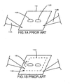
- the limited prior art relating to multiple scanning probes for FA shows the probes scanning one at a time in order to avoid collisions. This method is effective at avoiding collisions, at least until the probes move to their respective features of interest. However, this method takes longer to perform the scanning. This allows more time for drift, such as thermal drift, to occur. Also, the simple fact of longer measurement time is a serious weakness of the prior art.
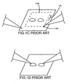
- FIG. 1c show different scanning directions, as is common in the prior art.
- FIG. 1d shows the scanning probe tips 114 positioned on the features of interest 112 and ready for an FA experiment. This process took twice the amount of time as was required for one scan. Similarly, if more probes are needed in the experiment the time delay scales with the number of probes used.
- This process also requires a difficult initial gross positioning setup.
- the scanning probes tips When the scanning probes tips are initially placed, they must be sufficiently far apart so that when one scanning probe tip is scanning, it does not collide with any other scanning probe tip that is not scanning. This requires initially placing the scanning probe tips sufficiently far apart to avoid the collision, and makes placing the scanning probe tips sufficiently close together to scan and image the same area difficult.
- US 6,028,305 describes a dual cantilever scanning probe microscope operating at high speeds where the two probes are part of the same probe assembly but one has a sharp tip used only at low speeds and high resolution configurations.
- a device and method to simultaneously scan multiple scanning probes over overlapping areas of interest to locate respective features of interest in a minimum amount of time employs at least two scanning probes, each probe supported by cantilever to an atomic force microscope (AFM).
- a controller in each AFM receives motion control signals from a master controller generating a first motion control signal for a first one of the AFMs for motion in a first axis and a second motion control signal for the first AFMs for motion in a second axis.
- the second axis is substantially perpendicular to the first axis.
- the master controller then calculates a first offset motion control signal responsive to the first motion control signal for a second one of the AFMs for motion in spaced relation to the first one of the AFMs in the first axis and a second offset motion control signal responsive to the second motion control signal for a second one of the AFMs for motion in spaced relation to the first one of the AFMs in the second axis.
- a scanning probe microscopy system comprising: at least two scanning probes, each probe supported by cantilever to an atomic force microscope (AFM); control means in each AFM adapted to receive motion control signals; means for generating a first motion control signal for a first one of the AFMs for motion in a first direction; means for generating a second motion control signal for the first one of the AFMs for motion in a second direction; means for determining a first offset motion control signal responsive to the first motion control signal for a second one of the AFMs for motion in spaced relation to the first one of the AFMs in the first direction; means for determining a second offset motion control signal responsive to the second motion control signal for the second one of the AFMs for motion over an overlapping scan area in spaced relation to the first one of the AFMs in the second direction; and, means for generating image scan data from input signals from each probe.
- AFM atomic force microscope
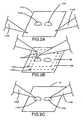
- an embodiment of the present invention employs two or more scanning probe tips 114a and 114b that are located near a sample 110.
- the sample 110 contains the features of interest 112a and 112b.
- Fig. 2b shows the scanning probe tips in relation to desired scan areas 116a and 116b respectively. Note that in the embodiment shown, the scan areas 116a and 116b are overlapping. Each scan area has a start point 118a and 118b where the respective scanning probe tip will begin its scan. Each scanning probe tip also has a scan direction 120a and 120b respectively. In the embodiment shown the scan directions 120a and 120b are always parallel and offset for all scanning probe tips. This provides for simultaneous motion of the probe tips in spaced relation thereby avoiding collision.
- FIG. 2c shows the scanning probe tips positioned on the features of interest and ready for an electrical measurement or force measurement.
- the scan waveforms are output to digital to analog converters (DACs) 140a, 140b and 140c respectively.
- DACs digital to analog converters
- the DACs share a clock signal 142 provided by clock generator 143 that ensures the scan waveforms remain synchronized.
- the DACs also share a synchronization pulse 144 provided by sync generator 145 that ensures that the scanning starts at the same time.
- the DACs drive control electronics 146a, 146b and 146c. Control electronics for SPM operation are well known to one skilled in the art. There is one complete, independent set of control electronics for each probe.
- the control electronics are each connected to an AFM head 148a, 148b and 148c respectively.
- Each AFM head contains a 3-axis actuator 150, a feedback position sensor 152 and a deflection sensor 154.
- the 3-axis actuator provides for scanning along the sample 110.
- the feedback position sensor 152 in conjunction with the control electronics provide calibrated scanning.
- the deflection sensor 154 in conjunction with 1-axis of the 3-axis actuator provides for constant force AFM scanning. This system may also be operated without force feedback, where the deflection sensor is used to generate the scan image.
- the control electronics generate the image data 157.
- the image data is passed to the analog to digital converters (ADCs) 158.
- the ADCs convert the image data to digital format pass the image to the computer.
- the computer can then display the image data to the user
- FIG. 5b shows a detailed side view of an embodiment of the probe tip employed with the present invention attached to a cantilever.
- the deflection sensor uses the reflective back of the cantilever to determine the deflection of the cantilever.
- the arrangement of the probe tip and cantilever shown allows the greatest clearance between multiple probes operating in close proximity.
- the angled attachment of the probe tip to the cantilever, or in alternative embodiments, the angling of the cantilever attachment to the AFM, to position the extreme end of the probe tip as far as possible from the AFM is employed to achieve this feature.
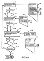
- FIG. 6 is a flow chart of the mathematical operations of the software.
- the standard SPM scan parameters input 159 consists of X scan size 160, Y scan size 162, X resolution 164, Y resolution 166, X offset 168 and Y offset 170 which are used by subsequent routines to create a scan waveform for the AFM manipulating each probe tip.
- the drive waveform generation routine 172 takes the SPM scan parameters input and outputs a drive waveform 174, identified as W, that contains both an X value output 176 and Y value output 178.
- the drive waveform is a triangle wave with the peaks and valleys rounded off, at the last 5 points.
- the waveform generation is accomplished in the following sequence.
- the X values of the drive waveform are centered about the value 'X offset'.
- the X values of the drive waveform have amplitude of 'X scan size' divided by 2.
- the X values of the drive waveform have the number of points per cycle equal to 2 multiplied by the value 'X resolution'.
- the X values of the drive waveform have a number of cycles equal to 2 times the value 'Y resolution'.
- the Y values of the drive waveform are centered about the value 'Y offset'.
- the Y values of the drive waveform have amplitude of 'Y scan size' divided by 2.
- the Y values of the drive waveform have the number of points per cycle equal to 2 multiplied by the value 'X resolution' multiplied by the value 'Y resolution'.
- the Y values of the drive waveform have 1 cycle.
- the X offset and Y offset values define the location of the scan area.
- the scan rotation routine 186 transforms the drive waveform W' to the spatial reference frame of the individual AFM heads 148.
- the input parameter platen angle R 187 for each AFM head and associated probe tip is the angle 122a, 122b or 122c of the probe tip centerline 124a, 124b or 124c, respectively, measured relative to the arbitrary reference axis 126 on the sample as described previously with respect to FIG. 4 .
- the output result of this routine is a rotated drive waveform W" 174" having an X value output 176" and a Y value output 178".
- a multiplication by a rotation transformation matrix M 189 formed based on an angle value equal to the platen angle R for each AFM probe tip, is performed.
- rotation is defined in the linear algebra context; to multiply by a matrix of the form given in the scan rotation routine to rotate the input array about the origin by the given angle.
- the data from the AFM control electronics 146 is gathered in step 195 and displayed as an image on the computer screen 132 to the user.
- a monitoring function 196 is concurrently checking if the user has selected the probe button on the computer screen 132. If the probe button has not been selected the scanning routine continues to gather data and update the display image. Note that in the embodiment shown the probe button is a software button and does not have a physical location. If the user has selected the probe button, reflected by operation 197, then the probe point routine takes the user's probing locations input, calculates a waveform 198 to move from the current location of the scanning probe tips to the user's probing locations and outputs the waveform, as reflected in routine 200, to the AFM control electronics.
- the scanning probe tips are moved by the AFM control electronics to the location specified by the user's probing location as shown in block 201.
- This routine is identical in function, but different in input to the start point positioning generation routine. The input to this function is the probing point, rather than the start point.
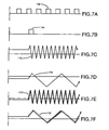
- FIGs. 7a through 7f show examples of some of the electrical signals during the execution of the scanning operation.
- FIG. 7a is the shared clock 142 that is used to make sure all AFMs remain synchronized.
- FIG. 7b shows the synchronization pulse 144 that signals for all AFMs to begin at the same time.
- FIG. 7c shows the X values of the drive waveform 176 generated by the waveform generation routine 172.
- FIG. 7d shows the Y values of the drive waveform 178 also generated by the waveform generation routine 172.
- FIG. 7e shows an example of the X values of the rotated drive waveform W" 188, for an AFM head that is rotated to an exemplary arbitrary platen angle relative to the sample 110.
- FIG. 7a is the shared clock 142 that is used to make sure all AFMs remain synchronized.
- FIG. 7b shows the synchronization pulse 144 that signals for all AFMs to begin at the same time.
- FIG. 7c shows the X values of the
- FIG. 7f shows an example of the Y values of the rotated drive waveform W" for the AFM head. These waveforms are generated by the scan rotation routine 186. Note that after the scan rotation routine 186 the rotated drive waveform 188, W', depend greatly on the platen angle 122.
- the system employs multiple scanning probe microscopes.
- the scanning probe tips may be in close proximity to one another, such as a few microns to under 1 micron. Additionally, the scanning probe tips are centered in their travel, engaged on a sample and may be able to scan an overlapping scan area. As previously described with respect to FIG. 2a, 2b, 2c , 3a, 3b, and 3c , the scan area 116 contains multiple features of interest 112.
- the drive waveforms W are rotated by the start point rotation routine 180 so that all scanning probe tips will start at the same point in their respective drive waveforms. This will ensure that the spacing between the AFM probe tips 114 will be constant for the start of scanning.
- the drive waveforms are rotated by the scan rotation routine 186 to result in the rotated drive waveforms W".
- This rotation ensures that even though all AFM heads and their associated scanning probe tips have a different platen angle they will all scan at the same direction at the same time and further ensures that the spacing between scanning probe tips will remain substantially constant for the duration of scanning.
- the rotated drive waveforms W" are loaded to the DACs 140a, 140b and 140c respectively.
- the AFMs are positioned placing the probe tips at the start points. Once the rotated drive waveforms have been loaded, all AFM control electronics share a common clock 142. This ensures that the scanning probe tips will stay synchronized. Then the synchronization circuit issues a synchronization pulse 144, which signals all AFM control electronics 146 to begin scanning. This ensures that all of the AFMs start scanning at the same time.
- the DACs then output their respective rotated drive waveform to their AFM control electronics. During scanning the scanning probe tips move in spaced relation to maintain constant spacing to when they first started scanning.
- Each set of AFM control electronics controls the feedback position sensors 152 and the 3-axis actuator 150 in the associated AFM head 148 to scan in a calibrated manner.
- Each deflection sensor 154 monitors the deflection of the cantilever 156 to which the scanning probe tip 114 is attached. This deflection signal is returned to the SPM control electronics 146 and displayed to the user on the computer screen 132.
- the AFM probe tips move in an identical scanning direction 120 at all times, as shown in FIGs. 2 a-c and 3a-c .
- the starting points 118a, 118b and 118c are in the same relative location for the scan areas 116a, 116b and 116c for all scanning probe tips.
- the spacing between the scanning probe tips is constant at all times.
- the computer 130 gathers data from the AFM control electronics 146 and displays it on the computer screen 132.
- the user locates the features of interest 112 on the computer screen, he or she can choose to probe those features.
- the user selects the location of the features of interest to be probed as the probing location 196 and selects the probe button 194.
- the computer 130 will calculate and output a waveform to the DACs 140 which will drive the AFM control electronics 146, which will drive the scanning probe tips to a respective point on the sample 110 corresponding to the probing location 196.
- the DACs 140 will share their common clocks 142 and synchronization pulse 144 as before.
- the DACs 140 will then drive the AFM control electronics 146. This will cause the scanning probe tips to move to the probing locations 196. Note that, for the first time since scanning began, the spacing between scanning probe tips 114 is no longer constant once the scanning probe tips 114 begin to move toward the probing locations 196.
- FIG. 8a shows the sample 110, features of interest 112a and 112b and an area to be avoided 198.
- the scanning probe tips 114a and 114b are positioned on the sample 110.
- Fig. 8b shows each of the scanning probe tips has its own scan area 116a and 116b, respectively, that excludes the area to be avoided 198.
- the spacing between scanning probe tips 114a and 114b may not always be constant.
- the probes retract in Z, the out of the plane of the sample direction, to avoid the area to be avoided.
- Each scan area 116 has a start point 118 that is where the scanning probe tip 114 will begin.
- Each scanning probe tip 114 also has a scanning direction 120. In the embodiment shown the scanning directions 120 are substantially the same for all probe tips 114.
- FIG. 9 shows in flow chart form the generation of the Z axis probe retraction waveform consistent with the area to be avoided which is overlaid on the waveform generation for the X and Y components of the AFM motion.
- FIGs. 10a, 10b show the waveforms of FIGs. 7c and 7d expanded and truncated for clarity.
- FIG. 10c show the corresponding Z axis actuation for the avoided area associated with the X and Y motion.
- the X and Y extents of the area to be avoided are provided as parameter input 202 to generation routine 204 for a control matrix 206 for the excluded area.
- a simple rectangular area is shown for the embodiment in the drawings, but is not a limitation on the invention.
- the control electronics monitor the X/Y position 208 of the probe tip as driven by the appropriate waveform 178 for X position and 176 for Y position shown in expanded form in FIGs. 10b and 10a respectively. If the probe tip position has entered the exclusion matrix values 210, the probe is lifted 212 by the Z axis control in the AFM. The X/Y position is then monitored to determine when the probe tip is clear of the exclusion matrix values 214 at which time the probe is lowered 216 to resume generation of image data.
- the exclusion area is graphically demonstrated in FIG. 10a as Y exclusion zone 218 and FIG. 10b as X exclusion zone 220.
- the resulting Z axis waveform 222 shown in FIG. 10c demonstrates the lifting of the probe tip when in the exclusion area.
- FIG. 8c shows the scanning probe tips 114 positioned on the features of interest 112 and ready for an FA experiment.
- a commercially available version of an embodiment of the invention is the Atomic Force Probe (AFP) system available from MultiProbe, Inc, 10 E. Islay Street, Santa Barbara, CA 93101, the assignee of the present application..
- This system is capable of placing the scanning probe tips in close proximity, being less than a few microns, as shown in FIG. 2c or 3c .
- This system has feedback position sensors 152 for the 3-axis actuator 150 and supporting SPM control electronics 146 as shown in FIG. 5 .
- This system also executes the software routine shown in block diagram form in FIG. 6 . For 3 scanning probe tips 114 this microscope performs the operation shown pictographically in FIG. 3 .
Landscapes
- Nuclear Medicine, Radiotherapy & Molecular Imaging (AREA)
- Physics & Mathematics (AREA)
- Health & Medical Sciences (AREA)
- General Health & Medical Sciences (AREA)
- General Physics & Mathematics (AREA)
- Radiology & Medical Imaging (AREA)
- Chemical & Material Sciences (AREA)
- Engineering & Computer Science (AREA)
- Nanotechnology (AREA)
- Analytical Chemistry (AREA)
- Crystallography & Structural Chemistry (AREA)
- Length Measuring Devices With Unspecified Measuring Means (AREA)
- Tests Of Electronic Circuits (AREA)
Claims (15)
- Rastersondenmikroskopiesystem, das Folgendes umfasst:mindestens zwei Rastersonden (114), wobei jede Sonde mittels eines Auslegers (156) an einem Rasterkraftmikroskop (AFM) (148a, 148b, 148c) gestützt ist;Steuermittel (150) in jedem AFM, die dafür ausgelegt sind, Bewegmgssteuersignale zu empfangen;Mittel zum Erzeugen eines ersten Bewegungssteuersignals (160, 164, 168, 172) für ein erstes der AFM zur Bewegung in einer ersten Richtung;Mittel zum Erzeugen eines zweiten Bewegungssteuersignals (162, 166, 170,172) für das erste der AFM zur Bewegung in einer zweiten Richtung;Mittel zum Bestimmen eines ersten Versatzbewegmgssteuersignals (122a, 189, 186), das auf das erste Bewegungssteuersignal für ein zweites der AFM zur Bewegung in einem beabstandeten Verhältnis zum ersten der AFM in der ersten Richtung reagiert;Mittel zum Bestimmen eines zweiten Versatzbewegungssteuersignals (122b, 189, 186), das auf das zweite Bewegungssteuersignal für das zweite der AFM zur Bewegung über einen überlappenden Abstastbereich in einem beabstandeten Verhältnis zum ersten der AFM in der zweiten Richtung reagiert; undMittel zum Erzeugen von Bildabtastdaten (137) von Eingangssignalen von jeder Sonde (114).
- Rastersondenmikroskopiesystem nach Anspruch 1, das ferner ein Rüclüneldungsmittel (152) von jeder Sonde zu dem jeweiligen Steuermittel zur Anpassung der zugehörigen Bewegmgssteuersignale umfasst.
- Rastersondenmikroskopiesystem nach Anspruch 1, wobei das Mittel zum Bestimmen eines ersten Versatzbewegungssteuersignals und das Mittel zum Bestimmen eines zweiten Versatzbewegungssteuersignals eine Rotationsmatrix (189) umfasst.
- Rastersondenmikroskopiesystem nach Anspruch 1, wobei jede Sonde (114) und der jeweilige Ausleger (156) für die Anordnung einer Spitze der Sonde distal zum AFM ausgerichtet sind.
- Rastersondenmikroskopiesystem nach Anspruch 1, wobei ein Auslegerablenkungssignal (154) überwacht wird und das Auslegerablenkungssignal das Eingangssignal von jeder Sonde zum Abtastbilderzeugungsmittel umfasst.
- Rastersondenmikroskopiesystem nach Anspruch 1, wobei ein Auslegerablenkungssignal (154) überwacht wird und das Auslegerablenkungssignal dem AFM eine Rückmeldung für eine Konstantkraftabtastung bereitstellt.
- Verfahren für die Rastersondenmikroslcopie, das folgende Schritte umfasst:Anbringen einer ersten Sonde (114), die von einem Ausleger (156) gestützt wird, an einem ersten AFM (148a),Anbringen einer zweiten Sonde (114), die von einem Ausleger (156) gestützt wird, an einem zweiten AFM (148b),Bestimmen einer ersten Richtcharakteristik für die erste Sonde;Bestimmen einer zweiten Richtcharakteristik für die erste Sonde;Berechnen eines ersten Steuersignals (160, 164, 168, 172), das der ersten Richtcharakteristik entspricht;Berechnen eines zweiten Steuersignals (162, 166, 170, 172), das der zweiten Richtcharakteristik entspricht;Bestimmen einer relativen Position der zweiten Sonde und des zweiten AFM (148a) zu der ersten Sonde und dem ersten AFM (148b);Berechnen eines ersten Versatzsteuersignals (122a, 189, 186) basierend auf dem ersten Steuersignal und der relativen Position der Bewegung der zweiten Sonde über einen überlappenden Abtastbereich in einem beabstandeten Verhältnis zu der ersten Sonde in der ersten Richtcharakteristik;Berechnen eines zweiten Versatzsteuersignals (122b, 189, 186) basierend auf dem zweiten Steuersignal und der relativen Position der Bewegung der zweiten Sonde über einen überlappenden Abtastbereich in einem beabstandeten Verhältnis zu der ersten Sonde in der zweiten Richtcharakteristik; undgleichzeitiges Anlegen des ersten und zweiten Steuersignals (160, 162, 164, 166, 168, 170, 172) an das erste AFM (148a) und der ersten und zweiten Versatzsteuerung (122a, 122b, 189, 186) an das zweite AFM (148b), undErzeugen von Bildabtastdaten (137) aus Eingaben von den Sonden.
- Verfahren für die Rastersondenmikroskopie nach Anspruch 7, das ferner folgende Schritte umfasst:Bereitstellen einer Rückmeldung für die Position der ersten Sonde;Modifizieren des ersten und zweiten Steuersignals als Reaktion auf die Rückmeldung;Bereitstellen einer zweiten Rückmeldung für die Position der zweiten Sonde; undModifizieren des ersten und zweiten Versatzsteuersignals als Reaktion auf die zweite Rückmeldung.
- Verfahren für die Rastersondenmikroskopie nach Anspruch 7, wobei
der Schritt des Anbringens einer ersten von einem Ausleger gestützten Sonde ferner den anfänglichen Schritt des Anbringens einer ersten Sonde und eines Auslegers in einem Winkel zur maximalen Beabstandung der ersten Sondenspitze von dem ersten AFM umfasst und der Schritt des Anbringens einer zweiten von einem Ausleger gestützten Sonde ferner den anfänglichen Schritt des Anbringens einer zweiten Sonde und eines Auslegers in einem Winkel zur maximalen Beabstandung der zweiten Sondenspitze von dem zweiten AFM umfasst. - Verfahren für die Rastersondenmikroskopie nach Anspruch 7, das ferner folgende Schritte umfasst:Überwachen eines Auslegerablenkungssignals für jede Sonde, undBereitstellen des Auslegerablenkungssignals zur Erzeugung der Bilddaten.
- Verfahren für die Rastersondenmikroskopie nach Anspruch 7, das ferner folgende Schritte umfasst:Überwachen eines Auslegerablenkungssignals für jede Sonde, undBereitstellung des Auslegerablenkungssignals als Rückmeldung zum AFM für die Sonde für eine Konstantkraftabtastung.
- Verfahren für die Rastersondenmikroskopie nach Anspruch 7, das ferner folgende Schritte umfasst:Auswählen einer Position für das Sondieren aus den erzeugten Bildabtastdaten, undAntreiben mindestens einer Sondenspitze zu der gewählten Position.
- Verfahren für die Rastersondenmikroskopie nach Anspruch 12, wobei der Schritt des Auswählens einer Position den Schritt der Auswahl einer Sondentaste umfasst.
- Verfahren für die Rastersondenmikroskopie nach Anspruch 12, wobei der Schritt des Antreibens die Schritte des Berechnens und der Ausgabe einer Wellenform zum Antreiben des AFM umfasst, das der mindestens einen Sondenspitze zugeordnet ist.
- Verfahren für die Rastersondenmikroskopie nach Anspruch 14, wobei eine zweite Sondenspitze basierend auf der ausgewählten Position angetrieben wird und der Schritt des Antreibens ferner den Schritt der gemeinsamen Nutzung gemeinsamer Taktsignale und eines gemeinsamen Synchronisationsimpulses für den Antrieb des ersten AFM für die erste Sondenspitze und des zweiten AFM für die zweite Sondenspitze umfasst.
Applications Claiming Priority (3)
| Application Number | Priority Date | Filing Date | Title |
|---|---|---|---|
| US39441402P | 2002-07-08 | 2002-07-08 | |
| US394414P | 2002-07-08 | ||
| PCT/US2003/021223 WO2004006302A2 (en) | 2002-07-08 | 2003-07-07 | Software synchronization of multiple scanning probes |
Publications (3)
| Publication Number | Publication Date |
|---|---|
| EP1520292A2 EP1520292A2 (de) | 2005-04-06 |
| EP1520292A4 EP1520292A4 (de) | 2008-05-21 |
| EP1520292B1 true EP1520292B1 (de) | 2013-10-09 |
Family
ID=30115719
Family Applications (1)
| Application Number | Title | Priority Date | Filing Date |
|---|---|---|---|
| EP03763297.3A Expired - Lifetime EP1520292B1 (de) | 2002-07-08 | 2003-07-07 | Softwaresynchronisation mehrerer rastersonden |
Country Status (6)
| Country | Link |
|---|---|
| US (3) | US6880389B2 (de) |
| EP (1) | EP1520292B1 (de) |
| JP (1) | JP4628099B2 (de) |
| CN (1) | CN100477067C (de) |
| AU (1) | AU2003256451A1 (de) |
| WO (1) | WO2004006302A2 (de) |
Families Citing this family (29)
| Publication number | Priority date | Publication date | Assignee | Title |
|---|---|---|---|---|
| EP1520292B1 (de) * | 2002-07-08 | 2013-10-09 | Multiprobe, Inc. | Softwaresynchronisation mehrerer rastersonden |
| US7633655B2 (en) * | 2003-10-10 | 2009-12-15 | Yuping Yang | Optical imaging device |
| US7415868B2 (en) * | 2005-03-21 | 2008-08-26 | Multiprobe, Inc. | Deconvolving tip artifacts using multiple scanning probes |
| US7205237B2 (en) * | 2005-07-05 | 2007-04-17 | International Business Machines Corporation | Apparatus and method for selected site backside unlayering of si, GaAs, GaxAlyAszof SOI technologies for scanning probe microscopy and atomic force probing characterization |
| DE102006006255A1 (de) * | 2006-02-10 | 2007-08-23 | Atg Test Systems Gmbh | Fingertester zum Prüfen von unbestückten Leiterplatten und Verfahren zum Prüfen unbestückter Leiterplatten mit einem Fingertester |
| JP2007218803A (ja) * | 2006-02-17 | 2007-08-30 | Research Institute Of Biomolecule Metrology Co Ltd | 走査型プローブ顕微鏡システム及び観察方法 |
| US7406860B2 (en) | 2006-04-28 | 2008-08-05 | Seagate Technology Llc | Atomic force microscopy scanning and image processing |
| JP2009192216A (ja) * | 2006-07-28 | 2009-08-27 | National Institute For Materials Science | 走査型プローブ顕微鏡及びその探針相対位置測定方法 |
| JP2008089510A (ja) * | 2006-10-04 | 2008-04-17 | Research Institute Of Biomolecule Metrology Co Ltd | 走査型プローブ顕微鏡、走査型プローブ顕微鏡用のプローブ、及び検査方法 |
| JP4859789B2 (ja) * | 2007-08-22 | 2012-01-25 | 株式会社堀場製作所 | 走査型プローブ顕微鏡及びその探針衝突回避方法 |
| JP5226481B2 (ja) * | 2008-11-27 | 2013-07-03 | 株式会社日立ハイテクサイエンス | 自己変位検出型カンチレバーおよび走査型プローブ顕微鏡 |
| US8479308B2 (en) | 2009-06-23 | 2013-07-02 | Kyoto University | Scanning probe microscope and method for detecting proximity of probes thereof |
| US9586817B2 (en) | 2011-07-28 | 2017-03-07 | Seagate Technology Llc | Semi-auto scanning probe microscopy scanning |
| US20130081159A1 (en) * | 2011-07-29 | 2013-03-28 | Seagate Technology Llc | Advanced atomic force microscopy scanning for obtaining a true shape |
| GB201215546D0 (en) | 2012-08-31 | 2012-10-17 | Infinitesima Ltd | Multiple probe detection and actuation |
| JP6366704B2 (ja) | 2013-06-24 | 2018-08-01 | ディーシージー システムズ、 インコーポレイテッドDcg Systems Inc. | 局所的な試料の特性によって制御されるプロービングの適応モードを備えたプロービングを利用したデータ収集システム |
| CN107004554B (zh) | 2014-06-25 | 2019-06-04 | Fei埃法有限公司 | 使用在线纳米探测的贯穿工艺流程的芯片内和芯片间的电分析和过程控制 |
| KR101718900B1 (ko) * | 2015-02-11 | 2017-03-23 | 한국과학기술원 | 복수의 afm 탐침을 가지는 나노 구조체 스캔장치와 방법 |
| US9581617B2 (en) | 2015-02-11 | 2017-02-28 | Korea Advanced Institute Of Science And Technology | Apparatus for scanning nano structure with plural AFM probes and method thereof |
| WO2017079374A1 (en) | 2015-11-03 | 2017-05-11 | Board Of Regents, The University Of Texas System | Metrology devices for rapid specimen setup |
| WO2017079375A1 (en) * | 2015-11-03 | 2017-05-11 | Board Of Regents, The University Of Texas System | Metrology devices and methods for independently controlling a plurality of sensing probes |
| JP2018044791A (ja) * | 2016-09-12 | 2018-03-22 | 大日本印刷株式会社 | 走査型プローブ顕微鏡および走査型プローブ顕微鏡を用いた走査方法 |
| US10139429B2 (en) | 2017-03-24 | 2018-11-27 | Fei Company | Method for calibrating and imaging using multi-tip scanning probe microscope |
| CN106842000B (zh) * | 2017-03-31 | 2020-02-07 | 北京半导体专用设备研究所(中国电子科技集团公司第四十五研究所) | 飞针测试机运动防撞机构 |
| DE102017109455A1 (de) * | 2017-05-03 | 2018-11-08 | Carl Zeiss Microscopy Gmbh | Mikroskopsystem und Verfahren zur Zeitsteuerung von Abläufen in einem Mikroskopsystem |
| CN107907712B (zh) * | 2017-11-08 | 2019-10-25 | 中国科学院物理研究所 | 用于多探针stm的分时复用控制装置及多探针stm |
| CN112394199A (zh) * | 2019-08-16 | 2021-02-23 | 长鑫存储技术有限公司 | 原子力显微镜及其测量方法 |
| US10873339B1 (en) * | 2019-12-24 | 2020-12-22 | Ipgreat Incorporated | On-chip pattern generator for high speed digital-to-analog converter |
| NL2034580B1 (en) * | 2023-04-14 | 2024-10-21 | Nearfield Instr B V | Multi-head AFM for defect inspection and review |
Family Cites Families (19)
| Publication number | Priority date | Publication date | Assignee | Title |
|---|---|---|---|---|
| DE3679319D1 (de) * | 1986-05-27 | 1991-06-20 | Ibm | Speichereinheit mit direktem zugriff. |
| EP0646913B1 (de) * | 1987-08-25 | 1999-01-13 | Canon Kabushiki Kaisha | Tunnelstromkodierer |
| JP2566794B2 (ja) | 1987-10-15 | 1996-12-25 | セイコー電子工業株式会社 | 走査型トンネル顕微鏡の測定方法 |
| US4956817A (en) | 1988-05-26 | 1990-09-11 | Quanscan, Inc. | High density data storage and retrieval system |
| JPH0298896A (ja) * | 1988-10-05 | 1990-04-11 | Olympus Optical Co Ltd | 記憶装置 |
| US4924091A (en) | 1989-02-01 | 1990-05-08 | The Regents Of The University Of California | Scanning ion conductance microscope |
| JP2945090B2 (ja) * | 1990-07-09 | 1999-09-06 | キヤノン株式会社 | エンコーダ |
| JPH06201369A (ja) * | 1992-12-28 | 1994-07-19 | Matsushita Electric Ind Co Ltd | 走査プローブ顕微鏡のマルチプローブヘッド |
| JP3581421B2 (ja) * | 1995-02-23 | 2004-10-27 | キヤノン株式会社 | 情報処理装置 |
| JP4190582B2 (ja) * | 1997-05-20 | 2008-12-03 | 徹雄 大原 | 原子間測定技術 |
| CN2326970Y (zh) * | 1997-12-02 | 1999-06-30 | 中国科学院上海原子核研究所 | 一种用于扫描探针显微镜的针尖与样品间距调节装置 |
| US6028305A (en) * | 1998-03-25 | 2000-02-22 | Board Of Trustees Of The Leland Stanford Jr. University | Dual cantilever scanning probe microscope |
| JP2001024038A (ja) * | 1999-07-05 | 2001-01-26 | Hitachi Ltd | プローブの位置決め方法および装置およびこれを利用した部材の評価方法 |
| US6545492B1 (en) * | 1999-09-20 | 2003-04-08 | Europaisches Laboratorium Fur Molekularbiologie (Embl) | Multiple local probe measuring device and method |
| CN2392189Y (zh) * | 1999-11-10 | 2000-08-16 | 中国科学院金属研究所 | 扫描隧道显微镜功函数信息成像装置 |
| US6583411B1 (en) * | 2000-09-13 | 2003-06-24 | Europaisches Laboratorium Für Molekularbiologie (Embl) | Multiple local probe measuring device and method |
| US6516528B1 (en) * | 2000-10-24 | 2003-02-11 | Advanced Micro Devices, Inc. | System and method to determine line edge roughness and/or linewidth |
| JP3819230B2 (ja) * | 2000-10-31 | 2006-09-06 | シャープ株式会社 | マルチプローブ型走査プローブ顕微鏡装置およびそれを用いた試料表面評価方法 |
| EP1520292B1 (de) * | 2002-07-08 | 2013-10-09 | Multiprobe, Inc. | Softwaresynchronisation mehrerer rastersonden |
-
2003
- 2003-07-07 EP EP03763297.3A patent/EP1520292B1/de not_active Expired - Lifetime
- 2003-07-07 CN CNB038161400A patent/CN100477067C/zh not_active Expired - Lifetime
- 2003-07-07 AU AU2003256451A patent/AU2003256451A1/en not_active Abandoned
- 2003-07-07 WO PCT/US2003/021223 patent/WO2004006302A2/en not_active Ceased
- 2003-07-07 US US10/615,223 patent/US6880389B2/en not_active Expired - Lifetime
- 2003-07-07 JP JP2004519973A patent/JP4628099B2/ja not_active Expired - Lifetime
-
2004
- 2004-12-17 US US11/015,945 patent/US6951130B2/en not_active Expired - Fee Related
-
2005
- 2005-09-29 US US11/240,090 patent/US7444857B2/en not_active Expired - Lifetime
Also Published As
| Publication number | Publication date |
|---|---|
| US20040025578A1 (en) | 2004-02-12 |
| EP1520292A2 (de) | 2005-04-06 |
| US6880389B2 (en) | 2005-04-19 |
| US20060032296A1 (en) | 2006-02-16 |
| WO2004006302A3 (en) | 2004-05-13 |
| EP1520292A4 (de) | 2008-05-21 |
| CN1666312A (zh) | 2005-09-07 |
| WO2004006302A2 (en) | 2004-01-15 |
| CN100477067C (zh) | 2009-04-08 |
| JP2005532555A (ja) | 2005-10-27 |
| JP4628099B2 (ja) | 2011-02-09 |
| AU2003256451A1 (en) | 2004-01-23 |
| AU2003256451A8 (en) | 2004-01-23 |
| US6951130B2 (en) | 2005-10-04 |
| US7444857B2 (en) | 2008-11-04 |
| US20050097944A1 (en) | 2005-05-12 |
Similar Documents
| Publication | Publication Date | Title |
|---|---|---|
| US6880389B2 (en) | Software synchronization of multiple scanning probes | |
| US8925376B2 (en) | Fully digitally controller for cantilever-based instruments | |
| EP1189240B1 (de) | Mehrfachsonden-Messgerät und zugehöriges Anwendungsverfahren | |
| US20030233870A1 (en) | Multidimensional sensing system for atomic force microscopy | |
| SG192224A1 (en) | Adaptive mode scanning probe microscope | |
| US8812976B2 (en) | Programmable equipment configuration method and apparatus | |
| EP2063250A1 (de) | Rasterkraftmikroskop | |
| Juhas et al. | A platform for micropositioning based on piezo legs | |
| KR101031135B1 (ko) | 복수의 스캐닝 프로브들의 소프트웨어 동기화 | |
| JP2002206999A (ja) | 走査型プローブ顕微鏡 | |
| JPH10213636A (ja) | 原子間力顕微鏡法を使用した電気波形を測定する方法及び装置 | |
| JP2002372488A (ja) | 走査型プローブ顕微鏡の探針接近方法 | |
| Hensel et al. | Computerized control system and interface for flexible micromanipulator control | |
| JP4602284B2 (ja) | 走査型プローブ顕微鏡 | |
| JP3942915B2 (ja) | 走査型プローブ顕微鏡を用いた基板上の試料を発見する方法、走査型プローブ顕微鏡を用いた基板上の試料を移動させる方法、及び走査型プローブ顕微鏡 | |
| JP2000275159A (ja) | 走査型プローブ顕微鏡の画像表示方法 | |
| JP2000214175A (ja) | 走査型プロ―ブ顕微鏡の測定方法 | |
| JP2005308687A (ja) | 走査型プローブ顕微鏡及び圧電素子の準備動作方法 | |
| JPS6243053A (ja) | ストロボ電子ビ−ム装置 | |
| JPH0668834A (ja) | トンネルスペクトロスコピー | |
| JP2001099773A (ja) | 走査型プローブ顕微鏡とその測定方法 | |
| JPH0231160A (ja) | マイクロマニピュレータ | |
| JPH0318703A (ja) | 走査形トンネル顕微鏡 | |
| JPH04238202A (ja) | 走査型プローブ顕微鏡およびその制御方法 | |
| JPH05203407A (ja) | 走査型トンネル顕微鏡 |
Legal Events
| Date | Code | Title | Description |
|---|---|---|---|
| PUAI | Public reference made under article 153(3) epc to a published international application that has entered the european phase |
Free format text: ORIGINAL CODE: 0009012 |
|
| 17P | Request for examination filed |
Effective date: 20041207 |
|
| AK | Designated contracting states |
Kind code of ref document: A2 Designated state(s): AT BE BG CH CY CZ DE DK EE ES FI FR GB GR HU IE IT LI LU MC NL PT RO SE SI SK TR |
|
| AX | Request for extension of the european patent |
Extension state: AL LT LV MK |
|
| REG | Reference to a national code |
Ref country code: DE Ref legal event code: R079 Ref document number: 60345060 Country of ref document: DE Free format text: PREVIOUS MAIN CLASS: H01L0021000000 Ipc: H01J0037000000 |
|
| RIC1 | Information provided on ipc code assigned before grant |
Ipc: 7G 01B 5/28 B Ipc: 7H 01J 37/00 A Ipc: 7H 01J 3/14 B |
|
| DAX | Request for extension of the european patent (deleted) | ||
| A4 | Supplementary search report drawn up and despatched |
Effective date: 20080422 |
|
| RIC1 | Information provided on ipc code assigned before grant |
Ipc: H01J 37/00 20060101AFI20050606BHEP Ipc: G01N 13/16 20060101ALI20080411BHEP Ipc: H01J 3/14 20060101ALI20080411BHEP Ipc: G12B 21/20 20060101ALI20080411BHEP |
|
| 17Q | First examination report despatched |
Effective date: 20090814 |
|
| REG | Reference to a national code |
Ref country code: DE Ref legal event code: R079 Ref document number: 60345060 Country of ref document: DE Free format text: PREVIOUS MAIN CLASS: H01J0037000000 Ipc: G01Q0010060000 |
|
| GRAP | Despatch of communication of intention to grant a patent |
Free format text: ORIGINAL CODE: EPIDOSNIGR1 |
|
| RIC1 | Information provided on ipc code assigned before grant |
Ipc: G01Q 70/06 20100101ALI20130315BHEP Ipc: G01Q 10/06 20100101AFI20130315BHEP Ipc: G01Q 30/04 20100101ALI20130315BHEP Ipc: B82Y 35/00 20110101ALN20130315BHEP |
|
| RIC1 | Information provided on ipc code assigned before grant |
Ipc: G01Q 70/06 20100101ALI20130403BHEP Ipc: G01Q 30/04 20100101ALI20130403BHEP Ipc: G01Q 10/06 20100101AFI20130403BHEP Ipc: B82Y 35/00 20110101ALN20130403BHEP |
|
| INTG | Intention to grant announced |
Effective date: 20130423 |
|
| GRAS | Grant fee paid |
Free format text: ORIGINAL CODE: EPIDOSNIGR3 |
|
| GRAA | (expected) grant |
Free format text: ORIGINAL CODE: 0009210 |
|
| AK | Designated contracting states |
Kind code of ref document: B1 Designated state(s): AT BE BG CH CY CZ DE DK EE ES FI FR GB GR HU IE IT LI LU MC NL PT RO SE SI SK TR |
|
| REG | Reference to a national code |
Ref country code: GB Ref legal event code: FG4D |
|
| REG | Reference to a national code |
Ref country code: CH Ref legal event code: EP Ref country code: AT Ref legal event code: REF Ref document number: 635783 Country of ref document: AT Kind code of ref document: T Effective date: 20131015 |
|
| REG | Reference to a national code |
Ref country code: IE Ref legal event code: FG4D |
|
| REG | Reference to a national code |
Ref country code: DE Ref legal event code: R096 Ref document number: 60345060 Country of ref document: DE Effective date: 20131205 |
|
| REG | Reference to a national code |
Ref country code: AT Ref legal event code: MK05 Ref document number: 635783 Country of ref document: AT Kind code of ref document: T Effective date: 20131009 |
|
| REG | Reference to a national code |
Ref country code: NL Ref legal event code: VDEP Effective date: 20131009 |
|
| PG25 | Lapsed in a contracting state [announced via postgrant information from national office to epo] |
Ref country code: SI Free format text: LAPSE BECAUSE OF FAILURE TO SUBMIT A TRANSLATION OF THE DESCRIPTION OR TO PAY THE FEE WITHIN THE PRESCRIBED TIME-LIMIT Effective date: 20131009 |
|
| PG25 | Lapsed in a contracting state [announced via postgrant information from national office to epo] |
Ref country code: NL Free format text: LAPSE BECAUSE OF FAILURE TO SUBMIT A TRANSLATION OF THE DESCRIPTION OR TO PAY THE FEE WITHIN THE PRESCRIBED TIME-LIMIT Effective date: 20131009 Ref country code: SE Free format text: LAPSE BECAUSE OF FAILURE TO SUBMIT A TRANSLATION OF THE DESCRIPTION OR TO PAY THE FEE WITHIN THE PRESCRIBED TIME-LIMIT Effective date: 20131009 Ref country code: FI Free format text: LAPSE BECAUSE OF FAILURE TO SUBMIT A TRANSLATION OF THE DESCRIPTION OR TO PAY THE FEE WITHIN THE PRESCRIBED TIME-LIMIT Effective date: 20131009 Ref country code: BE Free format text: LAPSE BECAUSE OF FAILURE TO SUBMIT A TRANSLATION OF THE DESCRIPTION OR TO PAY THE FEE WITHIN THE PRESCRIBED TIME-LIMIT Effective date: 20131009 |
|
| PG25 | Lapsed in a contracting state [announced via postgrant information from national office to epo] |
Ref country code: CY Free format text: LAPSE BECAUSE OF FAILURE TO SUBMIT A TRANSLATION OF THE DESCRIPTION OR TO PAY THE FEE WITHIN THE PRESCRIBED TIME-LIMIT Effective date: 20131009 Ref country code: ES Free format text: LAPSE BECAUSE OF FAILURE TO SUBMIT A TRANSLATION OF THE DESCRIPTION OR TO PAY THE FEE WITHIN THE PRESCRIBED TIME-LIMIT Effective date: 20131009 Ref country code: AT Free format text: LAPSE BECAUSE OF FAILURE TO SUBMIT A TRANSLATION OF THE DESCRIPTION OR TO PAY THE FEE WITHIN THE PRESCRIBED TIME-LIMIT Effective date: 20131009 |
|
| PG25 | Lapsed in a contracting state [announced via postgrant information from national office to epo] |
Ref country code: PT Free format text: LAPSE BECAUSE OF FAILURE TO SUBMIT A TRANSLATION OF THE DESCRIPTION OR TO PAY THE FEE WITHIN THE PRESCRIBED TIME-LIMIT Effective date: 20140210 |
|
| REG | Reference to a national code |
Ref country code: DE Ref legal event code: R097 Ref document number: 60345060 Country of ref document: DE |
|
| PG25 | Lapsed in a contracting state [announced via postgrant information from national office to epo] |
Ref country code: EE Free format text: LAPSE BECAUSE OF FAILURE TO SUBMIT A TRANSLATION OF THE DESCRIPTION OR TO PAY THE FEE WITHIN THE PRESCRIBED TIME-LIMIT Effective date: 20131009 |
|
| PLBE | No opposition filed within time limit |
Free format text: ORIGINAL CODE: 0009261 |
|
| STAA | Information on the status of an ep patent application or granted ep patent |
Free format text: STATUS: NO OPPOSITION FILED WITHIN TIME LIMIT |
|
| PG25 | Lapsed in a contracting state [announced via postgrant information from national office to epo] |
Ref country code: RO Free format text: LAPSE BECAUSE OF FAILURE TO SUBMIT A TRANSLATION OF THE DESCRIPTION OR TO PAY THE FEE WITHIN THE PRESCRIBED TIME-LIMIT Effective date: 20131009 Ref country code: CZ Free format text: LAPSE BECAUSE OF FAILURE TO SUBMIT A TRANSLATION OF THE DESCRIPTION OR TO PAY THE FEE WITHIN THE PRESCRIBED TIME-LIMIT Effective date: 20131009 Ref country code: SK Free format text: LAPSE BECAUSE OF FAILURE TO SUBMIT A TRANSLATION OF THE DESCRIPTION OR TO PAY THE FEE WITHIN THE PRESCRIBED TIME-LIMIT Effective date: 20131009 Ref country code: IT Free format text: LAPSE BECAUSE OF FAILURE TO SUBMIT A TRANSLATION OF THE DESCRIPTION OR TO PAY THE FEE WITHIN THE PRESCRIBED TIME-LIMIT Effective date: 20131009 |
|
| 26N | No opposition filed |
Effective date: 20140710 |
|
| PG25 | Lapsed in a contracting state [announced via postgrant information from national office to epo] |
Ref country code: DK Free format text: LAPSE BECAUSE OF FAILURE TO SUBMIT A TRANSLATION OF THE DESCRIPTION OR TO PAY THE FEE WITHIN THE PRESCRIBED TIME-LIMIT Effective date: 20131009 |
|
| REG | Reference to a national code |
Ref country code: DE Ref legal event code: R097 Ref document number: 60345060 Country of ref document: DE Effective date: 20140710 |
|
| PG25 | Lapsed in a contracting state [announced via postgrant information from national office to epo] |
Ref country code: LU Free format text: LAPSE BECAUSE OF FAILURE TO SUBMIT A TRANSLATION OF THE DESCRIPTION OR TO PAY THE FEE WITHIN THE PRESCRIBED TIME-LIMIT Effective date: 20140707 |
|
| REG | Reference to a national code |
Ref country code: CH Ref legal event code: PL |
|
| REG | Reference to a national code |
Ref country code: IE Ref legal event code: MM4A |
|
| PG25 | Lapsed in a contracting state [announced via postgrant information from national office to epo] |
Ref country code: LI Free format text: LAPSE BECAUSE OF NON-PAYMENT OF DUE FEES Effective date: 20140731 Ref country code: CH Free format text: LAPSE BECAUSE OF NON-PAYMENT OF DUE FEES Effective date: 20140731 |
|
| PG25 | Lapsed in a contracting state [announced via postgrant information from national office to epo] |
Ref country code: IE Free format text: LAPSE BECAUSE OF NON-PAYMENT OF DUE FEES Effective date: 20140707 |
|
| PG25 | Lapsed in a contracting state [announced via postgrant information from national office to epo] |
Ref country code: MC Free format text: LAPSE BECAUSE OF FAILURE TO SUBMIT A TRANSLATION OF THE DESCRIPTION OR TO PAY THE FEE WITHIN THE PRESCRIBED TIME-LIMIT Effective date: 20131009 |
|
| PG25 | Lapsed in a contracting state [announced via postgrant information from national office to epo] |
Ref country code: BG Free format text: LAPSE BECAUSE OF FAILURE TO SUBMIT A TRANSLATION OF THE DESCRIPTION OR TO PAY THE FEE WITHIN THE PRESCRIBED TIME-LIMIT Effective date: 20131009 |
|
| PG25 | Lapsed in a contracting state [announced via postgrant information from national office to epo] |
Ref country code: GR Free format text: LAPSE BECAUSE OF FAILURE TO SUBMIT A TRANSLATION OF THE DESCRIPTION OR TO PAY THE FEE WITHIN THE PRESCRIBED TIME-LIMIT Effective date: 20140110 |
|
| REG | Reference to a national code |
Ref country code: FR Ref legal event code: PLFP Year of fee payment: 14 |
|
| PG25 | Lapsed in a contracting state [announced via postgrant information from national office to epo] |
Ref country code: TR Free format text: LAPSE BECAUSE OF FAILURE TO SUBMIT A TRANSLATION OF THE DESCRIPTION OR TO PAY THE FEE WITHIN THE PRESCRIBED TIME-LIMIT Effective date: 20131009 Ref country code: HU Free format text: LAPSE BECAUSE OF FAILURE TO SUBMIT A TRANSLATION OF THE DESCRIPTION OR TO PAY THE FEE WITHIN THE PRESCRIBED TIME-LIMIT; INVALID AB INITIO Effective date: 20030707 |
|
| REG | Reference to a national code |
Ref country code: FR Ref legal event code: PLFP Year of fee payment: 15 |
|
| REG | Reference to a national code |
Ref country code: FR Ref legal event code: PLFP Year of fee payment: 16 |
|
| PGFP | Annual fee paid to national office [announced via postgrant information from national office to epo] |
Ref country code: GB Payment date: 20220727 Year of fee payment: 20 Ref country code: DE Payment date: 20220725 Year of fee payment: 20 |
|
| PGFP | Annual fee paid to national office [announced via postgrant information from national office to epo] |
Ref country code: FR Payment date: 20220725 Year of fee payment: 20 |
|
| REG | Reference to a national code |
Ref country code: DE Ref legal event code: R071 Ref document number: 60345060 Country of ref document: DE |
|
| REG | Reference to a national code |
Ref country code: GB Ref legal event code: PE20 Expiry date: 20230706 |
|
| PG25 | Lapsed in a contracting state [announced via postgrant information from national office to epo] |
Ref country code: GB Free format text: LAPSE BECAUSE OF EXPIRATION OF PROTECTION Effective date: 20230706 |