US8479308B2 - Scanning probe microscope and method for detecting proximity of probes thereof - Google Patents
Scanning probe microscope and method for detecting proximity of probes thereof Download PDFInfo
- Publication number
- US8479308B2 US8479308B2 US13/380,261 US201013380261A US8479308B2 US 8479308 B2 US8479308 B2 US 8479308B2 US 201013380261 A US201013380261 A US 201013380261A US 8479308 B2 US8479308 B2 US 8479308B2
- Authority
- US
- United States
- Prior art keywords
- probe
- tuning
- probes
- vibration
- proximity
- Prior art date
- Legal status (The legal status is an assumption and is not a legal conclusion. Google has not performed a legal analysis and makes no representation as to the accuracy of the status listed.)
- Expired - Fee Related
Links
- 239000000523 sample Substances 0.000 title claims abstract description 834
- 238000000034 method Methods 0.000 title claims description 39
- 230000008859 change Effects 0.000 claims abstract description 28
- 238000001514 detection method Methods 0.000 claims description 21
- 238000012544 monitoring process Methods 0.000 claims description 4
- 230000000087 stabilizing effect Effects 0.000 claims description 4
- 239000013078 crystal Substances 0.000 abstract description 37
- 230000007246 mechanism Effects 0.000 description 33
- 230000003287 optical effect Effects 0.000 description 22
- 238000004020 luminiscence type Methods 0.000 description 15
- 238000010586 diagram Methods 0.000 description 12
- 238000005259 measurement Methods 0.000 description 12
- 230000007423 decrease Effects 0.000 description 11
- 239000000969 carrier Substances 0.000 description 10
- 230000009977 dual effect Effects 0.000 description 10
- 238000002474 experimental method Methods 0.000 description 9
- 239000010931 gold Substances 0.000 description 9
- 239000004065 semiconductor Substances 0.000 description 8
- 238000013459 approach Methods 0.000 description 7
- PCHJSUWPFVWCPO-UHFFFAOYSA-N gold Chemical compound [Au] PCHJSUWPFVWCPO-UHFFFAOYSA-N 0.000 description 7
- 229910052737 gold Inorganic materials 0.000 description 7
- 238000010200 validation analysis Methods 0.000 description 7
- 238000012545 processing Methods 0.000 description 6
- 238000012360 testing method Methods 0.000 description 6
- 239000011248 coating agent Substances 0.000 description 5
- 238000000576 coating method Methods 0.000 description 5
- 230000005284 excitation Effects 0.000 description 5
- 239000000835 fiber Substances 0.000 description 5
- 230000003993 interaction Effects 0.000 description 5
- 230000010355 oscillation Effects 0.000 description 5
- 230000006798 recombination Effects 0.000 description 4
- 238000005215 recombination Methods 0.000 description 4
- 230000001360 synchronised effect Effects 0.000 description 4
- 239000013307 optical fiber Substances 0.000 description 3
- 238000004621 scanning probe microscopy Methods 0.000 description 3
- 238000012795 verification Methods 0.000 description 3
- 230000002238 attenuated effect Effects 0.000 description 2
- 230000003247 decreasing effect Effects 0.000 description 2
- 238000009792 diffusion process Methods 0.000 description 2
- 239000011159 matrix material Substances 0.000 description 2
- 230000000704 physical effect Effects 0.000 description 2
- 230000003863 physical function Effects 0.000 description 2
- 238000001878 scanning electron micrograph Methods 0.000 description 2
- 230000009471 action Effects 0.000 description 1
- 229910052782 aluminium Inorganic materials 0.000 description 1
- XAGFODPZIPBFFR-UHFFFAOYSA-N aluminium Chemical compound [Al] XAGFODPZIPBFFR-UHFFFAOYSA-N 0.000 description 1
- 238000013461 design Methods 0.000 description 1
- 230000000694 effects Effects 0.000 description 1
- 239000011521 glass Substances 0.000 description 1
- 238000005286 illumination Methods 0.000 description 1
- 239000002184 metal Substances 0.000 description 1
- 229910052751 metal Inorganic materials 0.000 description 1
- 230000008569 process Effects 0.000 description 1
- 230000000750 progressive effect Effects 0.000 description 1
- 230000000644 propagated effect Effects 0.000 description 1
- 230000003252 repetitive effect Effects 0.000 description 1
- 230000004044 response Effects 0.000 description 1
- 238000010079 rubber tapping Methods 0.000 description 1
- 230000035945 sensitivity Effects 0.000 description 1
Images


Classifications
-
- G—PHYSICS
- G01—MEASURING; TESTING
- G01Q—SCANNING-PROBE TECHNIQUES OR APPARATUS; APPLICATIONS OF SCANNING-PROBE TECHNIQUES, e.g. SCANNING PROBE MICROSCOPY [SPM]
- G01Q20/00—Monitoring the movement or position of the probe
- G01Q20/04—Self-detecting probes, i.e. wherein the probe itself generates a signal representative of its position, e.g. piezoelectric gauge
-
- G—PHYSICS
- G01—MEASURING; TESTING
- G01Q—SCANNING-PROBE TECHNIQUES OR APPARATUS; APPLICATIONS OF SCANNING-PROBE TECHNIQUES, e.g. SCANNING PROBE MICROSCOPY [SPM]
- G01Q10/00—Scanning or positioning arrangements, i.e. arrangements for actively controlling the movement or position of the probe
- G01Q10/04—Fine scanning or positioning
- G01Q10/045—Self-actuating probes, i.e. wherein the actuating means for driving are part of the probe itself, e.g. piezoelectric means on a cantilever probe
-
- G—PHYSICS
- G01—MEASURING; TESTING
- G01Q—SCANNING-PROBE TECHNIQUES OR APPARATUS; APPLICATIONS OF SCANNING-PROBE TECHNIQUES, e.g. SCANNING PROBE MICROSCOPY [SPM]
- G01Q10/00—Scanning or positioning arrangements, i.e. arrangements for actively controlling the movement or position of the probe
- G01Q10/04—Fine scanning or positioning
- G01Q10/06—Circuits or algorithms therefor
- G01Q10/065—Feedback mechanisms, i.e. wherein the signal for driving the probe is modified by a signal coming from the probe itself
-
- G—PHYSICS
- G01—MEASURING; TESTING
- G01Q—SCANNING-PROBE TECHNIQUES OR APPARATUS; APPLICATIONS OF SCANNING-PROBE TECHNIQUES, e.g. SCANNING PROBE MICROSCOPY [SPM]
- G01Q60/00—Particular types of SPM [Scanning Probe Microscopy] or microscopes; Essential components thereof
- G01Q60/18—SNOM [Scanning Near-Field Optical Microscopy] or apparatus therefor, e.g. SNOM probes
- G01Q60/22—Probes, their manufacture, or their related instrumentation, e.g. holders
-
- G—PHYSICS
- G01—MEASURING; TESTING
- G01Q—SCANNING-PROBE TECHNIQUES OR APPARATUS; APPLICATIONS OF SCANNING-PROBE TECHNIQUES, e.g. SCANNING PROBE MICROSCOPY [SPM]
- G01Q70/00—General aspects of SPM probes, their manufacture or their related instrumentation, insofar as they are not specially adapted to a single SPM technique covered by group G01Q60/00
- G01Q70/06—Probe tip arrays
Abstract
A scanning probe microscope includes: a first and second probes for scanning a sample while maintaining the distance to the sample surface; crystal oscillators holding each of the first and second probes; and a modulation oscillator for providing the first probe with a vibration of a specific frequency which is different from the resonant frequency of each crystal oscillator. A control unit monitors the vibration of the specific frequency of the first and second probes, detects proximity of the first probe and the second probe to each other based on the change of the specific frequencies, and controls the drive of the first and second probes.
Description
The present invention relates to a scanning probe microscope having a plurality of probes and a method for detecting the proximity of those probes. In particular, it relates to a scanning probe microscope for controlling the distance between the sample surface and the probe tip by a shear force method, and a method for detecting the proximity of its probes.
Scanning probe microscopy (SPM) is a technique for measuring in nanoscale the surface profile of a sample or a variety of physical properties and functions of the sample surface by scanning the sample surface with a sharp-pointed probe. In recent years, scanning probe microscopes having a plurality of probes have been developed with the aim of more accurately measuring the surface profile and a variety of physical properties and functions of a sample.
In such a scanning probe microscope having a plurality of probes, an optical microscope or an electron microscope is conventionally used to move the plurality of probes to the measurement position on the sample surface (refer to Patent Document 1).
In a scanning near-field optical microscope (SNOM), which is a kind of scanning probe microscope, a near-field light is generated around a probe positioned near a sample, and the light intensity or the optical characteristics of the scattered light generated by the interaction between the probe and the sample surface is measured to detect the surface condition of the sample. It is very important to accurately detect the distance between the sample surface and the probe tip and precisely control the position of the probe tip in order to realize a resolution beyond the diffraction limit of light.
[Patent Document 1] JP-A 2008-14903
In an SNOM, the distance between the sample surface and the probe tip or that between probes is sometimes set to be smaller than the diffraction limit of light. In such a case, it is impossible to control the position of the probe tip by monitoring it using an optical microscope. Although an electron microscope may be used to observe the distance between the sample surface and the probe tip or that between probes, it is troublesome and time-consuming.
In an SNOM with a single probe, the distance between the probe tip and the sample surface is controlled by using an interaction (shear force) that occurs therebetween when the probe tip and the sample surface are close to each other. However, this control method cannot be used in an SNOM having a plurality of probes, because, when probes are in proximity to each other, there is an influence of the shear force between the probes, which prevents an individual control of the position of each probe.
The problem to be solved by the present invention is to provide a scanning probe microscope capable of accurately controlling the relative distance among a plurality of probes and a method for detecting the proximity of its probes.
The present invention has been developed to solve the previously described problem, and the first aspect of the present invention provides a scanning probe microscope having a first probe and a second probe both for scanning a sample while maintaining a constant distance to a surface of the sample, including:
a) a first scanner for moving the first probe relative to the sample;
b) a second scanner for moving the second probe relative to the sample;
c) a vibrator for providing either the first probe or the second probe with a vibration of a specific frequency;
d) a vibration monitor for monitoring the vibration of the specific frequency of the first probe and the second probe;
e) a probe proximity detector for detecting proximity of the first probe and the second probe to each other based on a change of at least either a vibration of the first probe or a vibration of the second probe; and
f) a controller for controlling the first scanner and the second scanner based on a result of detection by the probe proximity detector.
The number of the first probe is not limited to one but may be plural. Similarly, the number of the second probe may be one or more than one.
In the first aspect of the present invention, the vibrator may provide the first probe with the vibration; and the probe proximity detector may detect proximity of the first probe and the second probe to each other based on the fact that a rate of change of the vibration of the first probe is equal to or less than a threshold. Alternatively, the probe proximity detector may detect proximity of the first probe and the second probe to each other based on the fact that a rate of change of the vibration of the second probe exceeds a threshold.
The second aspect of the present invention is a specific mode of the scanning probe microscope according to the first aspect of the present invention, wherein
the first probe and the second probe are attached to a first tuning-fork oscillator and a second tuning-fork oscillator, and the scanners move each of the first probe and the second probe while resonating each of the tuning-fork oscillators, and the scanning probe microscope including:
a voltage detector for detecting a voltage signal induced in each of the tuning-fork oscillators when a tip of the first probe and a tip of the second probe are individually approximated to the surface of the sample; and
a probe-sample distance controller for stabilizing a distance between the tip of each probe and the sample surface based on a result of detection by the voltage detector.
The third aspect of the present invention provides a scanning probe microscope having a first probe and a second probe both for scanning a sample while maintaining a constant distance to a surface of the sample, including:
a) a first tuning-fork oscillator to which the first probe is attached;
b) a second tuning-fork oscillator to which the second probe is attached;
c) a scanner for moving each of the first probe and the second probe relative to the sample while resonating each of the first tuning-fork oscillator and the second tuning-fork oscillator;
d) a vibrator for providing either the first probe or the second probe with a vibration of a specific frequency;
e) a signal detector for detecting a voltage signal of the specific frequency induced in each of the tuning-fork oscillators when the first probe and the second probe are approximated to each other while each of the first tuning-fork oscillator and the second tuning-fork oscillator is resonated; and
f) a probe proximity detector for detecting proximity of the first probe and the second probe to each other based on a voltage signal of the specific frequency induced in each of the first tuning-fork oscillator and the second tuning-fork oscillator.
In the third aspect of the present invention, the probe proximity detector may preferably detect proximity of the first probe and the second probe to each other based on the product of a voltage signal of the specific frequency induced in the first tuning-fork oscillator and a voltage signal of the specific frequency induced in the second tuning-fork oscillator.
Alternatively, in the third aspect of the present invention, the probe proximity detector may detect proximity of the first probe and the second probe to each other based on the sum of a voltage signal of the specific frequency induced in the first tuning-fork oscillator and a voltage signal of the specific frequency induced in the second tuning-fork oscillator.
In the second and third aspects of the present invention, the specific frequency may preferably be different from the resonance frequency of the tuning-fork oscillators.
The fourth aspect of the present invention provides a method for detecting proximity of probes of a scanning probe microscope having a first probe and a second probe both for scanning a sample while maintaining a constant distance to a surface of the sample, comprising the steps of:
providing either the first probe or the second probe with a vibration of a specific frequency; and
detecting proximity of the first probe and the second probe to each other by detecting the vibration of the specific frequency which is transmitted from the first probe to the second probe.
In particular, it is preferable that the proximity of the first probe and the second probe to each other is detected based on a change of at least either a vibration of the specific frequency of the first probe or a vibration of the specific frequency of the second probe.
The fifth aspect of the present invention provides a method for detecting proximity of probes of a scanning probe microscope having a first probe and a second probe both for scanning a sample while maintaining a constant distance to a surface of the sample, wherein:
the first probe is attached to a first tuning-fork oscillator;
the second probe is attached to a second tuning-fork oscillator;
a vibration of a specific frequency is provided to either the first probe or the second probe; and
proximity of the first probe and the second probe to each other is detected based on a voltage signal of the specific frequency induced in each of the first tuning-fork oscillator and the second tuning-fork oscillator.
In scanning the surface of a sample with a plurality of probes, when the plurality of probes are moved closer to each other, an interaction called the “shear force” occurs between the probes. This interaction affects the vibration state of each probe. In the scanning probe microscope of the present invention, while the first and second probes are being moved, a vibration of a specific frequency is provided to one of these probes, and the vibration of the specific frequency is monitored for both probes. The proximity of these probes is detected based on a change of the vibration of the specific frequency in at least one of these probes. Therefore, it is possible to prevent a collision of the first and second probes while these probes are being moved.
Hereinafter, concrete embodiments of the present invention will be described with reference to the figures.
Initially, the first embodiment of the present invention will be described with reference to FIGS. 1 through 22 . The scanning probe microscope (SPM) according to the present embodiment is a near-field optical microscope (SNOM). FIG. 1 shows a schematic configuration diagram of the scanning near-field optical microscope according to the present embodiment. As shown in FIG. 1 , the SNOM 1 of the first embodiment includes: a sample stage 3 on which a sample S is placed; a first probe 5 and a second probe 6 for scanning the surface of the sample S; a sample movement mechanism 8 for moving the sample stage 3 in the XY (horizontal) direction and in the Z (vertical) direction; a probe movement mechanism 10 for moving the first probe 5 in the XY (horizontal) direction and in the Z (vertical) direction; a distance control mechanism 12 for controlling the distance of the tips of the first probe 5 and the second probe 6 from the sample; a light source 14 for generating a laser light; and a detection unit 16 for detecting a signal light emitted from the sample. The detection unit 16 includes a condensing lens, a spectroscope, and a charge-coupled device (CCD).
The sample movement mechanism 8 is composed of a fine movement mechanism 18 driven with a piezo-actuator, and a rough movement mechanism 20 driven with a stepping motor. The sample movement mechanism 8 moves the sample stage 3 in the horizontal (XY) direction and in the vertical (Z) direction. The control unit 22 controls the sample movement mechanism 8 so as to selectively perform a relatively large movement with the rough movement mechanism 20 and a micro movement with the fine movement mechanism 18. By this mechanism, the sample placed on the sample stage 3 can be moved in the horizontal direction and in the vertical direction.
Both the first probe 5 and the second probe 6 are composed of an optical fiber probe having a sharp-pointed tip at which a micro opening with a diameter equal to or less than the wavelength to be taken out as a near-field light is formed. Each of the optical fiber probes is metal-coated (e.g. gold (Au) coated) except for their tips and openings.
The laser light emitted from the light source 14 is introduced into either the first probe 5 or the second probe 6 from an end thereof, and leaks out from the micro opening of the probe tip to form a near-field light on the sample surface. Meanwhile, the scattered light and other types of light generated on the sample surface by the near-field light formed on the sample surface are introduced into either the tip opening of the first probe 5 or that of the second probe 6, to be sent to the detection unit 16. The probe for guiding light from the light source 14 to the sample surface is called an illumination probe (I probe), and the probe for collecting lights generated on the sample surface and guiding them to the detection unit 16 is called a collection probe (C probe). In the SNOM 1 of the present embodiment, both the first probe 5 and the second probe 6 can be used as either the I probe or C probe.
The probe movement mechanism 10 is composed of a fine movement mechanism 10 a driven with a piezo-actuator and a rough movement mechanism 10 b driven with a stepping motor. The probe movement mechanism 10 moves the first probe 5 in the horizontal (XY) direction and in the vertical (Z) direction. The fine movement mechanism 10 a and the rough movement mechanism 10 b are connected to the control unit 22. The control unit 22 selectively performs a relatively large movement with the rough movement mechanism 10 b and a micro movement with the fine movement mechanism 10 a. In the present embodiment, the sample movement mechanism 8 and the probe movement mechanism 10 function as the first scanner, and the sample movement mechanism 8 functions as the second scanner.
The distance control mechanism 12 controls the distance between the tip of the first probe 5 and the sample surface as well as the distance between the tip of the second probe 6 and the sample surface by detecting the shear force acting between the sample surface and each of the tips of the first and second probes 5 and 6 while the first probe 5 and the second probe 6 being micro-vibrated are moved closer to the sample surface. In particular, the distance control mechanism 12 is composed of: tuning-fork (U-shaped) crystal oscillators 25 and 27; oscillators 29 and 30 respectively connected to the crystal oscillators 25 and 27; and lock-in amplifiers 32 and 34. Each of the crystal oscillators 25 and 27 has a U-shaped structure in which a pair of oscillating bodies is connected to each other. The pair of the oscillating bodies is electrically insulated. The oscillator 29 is electrically connected to one oscillating body of the crystal oscillator 25, and the oscillator 30 is electrically connected to one oscillating body of the crystal oscillator 27.
In FIG. 1 , the probes (the first probe 5 and the second probe 6) are fixed to the oscillating bodies to which the oscillators (the oscillator 29 and the oscillator 30) are respectively connected. However, the probes (the first probe 5 and the second probe 6) may be fixed to the oscillating bodies to which the lock-in amplifiers (the lock-in amplifier 32 and the lock-in amplifier 34) are connected.
A reference signal for performing a phase detection (synchronous detection) is provided from the oscillators 29 and 30 to the lock-in amplifiers 32 and 34.
When a voltage for vibration (alternating voltage) is applied from the oscillators 29 and 30 to the oscillating bodies, the oscillating bodies vibrate in the plane where the U-shaped structure of the tuning fork exists. In synchronization with this, the other oscillating body vibrates. With the frequency of the resonance point, they resonate with the greatest amplitude. At this point, the voltage induced in each of the oscillating bodies is measured in the lock-in amplifiers 32 and 34, and provided to the control unit 22.
In this state, the tips of the probes 5 and 6 are moved closer to the sample surface. When the distance between the tips of the probes 5 and 6 and the sample surface is not greater than a certain value, a shear force acts on the probes 5 and 6 and decreases the amplitude of their vibration, which decreases the amplitude of the oscillating bodies as well. As the amplitude of the oscillating bodies decreases, the amplitude of the voltage measured in the lock-in amplifiers 32 and 34 also decreases. The control unit 22 controls the probe movement mechanism 10 so as to maintain a constant amplitude of the voltage measured by the lock-in amplifier 32, and also controls the sample movement mechanism 8 so as to maintain a constant amplitude of the voltage measured by the lock-in amplifier 34. Thus, the present system can move the probes 5 and 6 while maintaining a constant distance between the tip of the probe 5 and the sample surface as well as between the tip of the probe 6 and the sample surface.
In the SNOM 1 of the present embodiment, the sample surface can be observed by using both the first probe 5 and the second probe 6, or by using only one of them. A mode for observing the sample surface by using either one of the first probe 5 and the second probe 6 as the I probe and the other probe as the C probe is called a dual IC mode. A mode for observing the sample surface by using only one of the first probe 5 and the second probe 6 is called an IC mode, I mode, or C mode. In the IC mode, one probe serves as the IC probe which serves as both the I probe and C probe; the probe for supplying a laser light from the light source 14 to the sample surface also serves as a guide for collecting the scattered light generated on the sample surface and sending it to the detection unit 16. In the C mode, either the first probe 5 or the second probe 6 serves as the C probe; the sample surface is irradiated with a light from a far field, and the scattered light or other types of light generated on the sample surface by the light is collected with the C probe. In the I mode, either the first probe 5 or the second probe 6 serves as the I probe; the sample surface is irradiated with a light by using the I probe, and the scattered light or other types of light generated by the light is broadly observed with a lens or other means.
For example, in the case where the sample S is a semiconductor, it can be observed in the previously described four modes as follows: In the C mode, the semiconductor is broadly irradiated with a light from a far field to excite carriers, and a local luminescence resulting from the recombination of the carriers is collected with the C probe to be observed. In the I mode, the semiconductor is locally irradiated with a light, and a luminescence from the excited carriers is broadly observed with a lens. In the IC mode or dual IC mode, the semiconductor is locally exited with the I probe or IC probe, and a locally collected light of the luminescence resulting from the recombination of the exited carriers can be observed with the C probe or IC probe.
In particular, in the dual IC mode, by moving the I probe and the C probe closer to each other, the luminescence from the carriers excited by the light from the I probe can be captured with the C probe. This allows an observation of the flow direction of the carriers, i.e. the carrier flow path. The carrier diffusion length in InGaN, which is a kind of semiconductor, is estimated to be about several hundreds of nm. In order to observe a carrier flow path of InGaN, the distance between the first and the second probes 5 and 6 has to be less than several hundreds of nm.
As just described, in the IC mode, I mode, and C mode, the sample surface is scanned with one probe. In the dual IC mode, the sample surface is scanned with two probes, and therefore it is necessary to control the distance between the probes as well as the distance between both probes and the sample. In particular, when the two probes 5 and 6 are moved closer to each other, it is necessary to control their movement so that they will not collide with each other. However, when the distance between the probes 5 and 6 is not more than a certain value, a shear force acts between the probes 5 and 6. Hence, it is necessary to take the influence of the shear force into consideration in controlling the movement of the probes 5 and 6.
Given this factor, in the SNOM 1 of the present embodiment, in performing a measurement in the dual IC mode, either the first probe 5 or the second probe 6, e.g. the first probe 5, is supplied with a vibration of a specific frequency (which will hereinafter be called a “modulated vibration”) which is different from the resonant frequency of the crystal oscillator 25. Then, the amplitude of the modulated vibration is detected for both the probes 5 and 6, and based on a change of the amplitude, it is determined that the two probes 5 and 6 are in proximity to each other.
Hereinafter, the processing flow of the dualband modulation control method will be described in detail.
For example, consider the case where the two objects of the probe B and the sample (surface) exist in the vicinity of the probe A. Let x and z be the distance from the probe A to the probe B and that to the sample, respectively. When C is the amplitude of the crystal oscillator (tuning fork), the actual oscillation can be expressed by
C cos ω1t.
In this case, suppose that the relationship between C, x and z is expressed by
C=fx(x)fz(z).
C cos ω1t.
In this case, suppose that the relationship between C, x and z is expressed by
C=fx(x)fz(z).
Function fx(x) is represents the relationship regarding the magnitude of the amplitude attenuation that the probe B gives to probe A, and function fz(z) represents the relationship regarding the magnitude of the amplitude attenuation that the sample surface gives to probe A. Both fx(x) and fz(z) are a monotonically decreasing function, and the differential functions fx(x) and fz(z) also monotonically decrease in the area where the distance between the probes A and B and the distance between the sample surface and the probe A are large to some extent. When the distance x is modulated with a frequency of ωm/2π and an amplitude of α, given that the amplitude α is sufficiently small, fx(x) can be expressed by the following approximation formula:
fx(x)=fx(x0)+af′x(x0)cos ωm t.
fx(x)=fx(x0)+af′x(x0)cos ωm t.
Hence, for example, the piezoelectric signal s(x, z, t)(=kC cos ω1t) of the tuning fork generated by the vibration of the crystal oscillator 27 will be:
s(x,z,t)=kfz(z)(fx(x0)+af′x(x0)cos ωm t)cos ωl t,
in which the modulated vibration and the resonant vibration are superimposed, where k is a proportional (physical) constant representing the relationship between the amplitude C of the crystal oscillator and the signal s(x, z, t).
s(x,z,t)=kfz(z)(fx(x0)+af′x(x0)cos ωm t)cos ωl t,
in which the modulated vibration and the resonant vibration are superimposed, where k is a proportional (physical) constant representing the relationship between the amplitude C of the crystal oscillator and the signal s(x, z, t).
The piezoelectric signal s(x, z, t) multiplied by cosω1 t of the reference signal which is in synchronization with the resonant vibration gives the following:
Passing this signal through a low-pass filter (LPF) 221 gives the resonant oscillation of only the frequency component which is the same as the resonant oscillation of the first term having an amplitude s1(x, z, t).
That is,
s 1(x,z,t)=(½)kfz(z)(fx(x0)+af′x(x0)cosωm t).
s 1(x,z,t)=(½)kfz(z)(fx(x0)+af′x(x0)cosωm t).
This signal s1(x, z, t) additionally contains a modulated signal component cos ωmt. This modulated signal component can be removed by passing the above signal through another LPF 222.
That is, s1(x, z)=(½)k fz(z)(fx(x0). is obtained.
This gives information s1(x, z) regarding the distance h between the second probe 6 and the sample surface and the distance d between the second probe 6 and the first probe 5.
Meanwhile, s1(x, z, t) multiplied by the modulated signal component cosωm t gives the following:
Passing this signal through a LPF 224 gives only the frequency component which is the same as the modulated signal of the second term (the amplitude s2(x, z) of the modulated vibration).
That is,
s 2(x,z)=(¼)kfz(z)af′x(x0)
is obtained
s 2(x,z)=(¼)kfz(z)af′x(x0)
is obtained
This signal s2(x, z) also includes the information on the distance h between the second probe 6 and the sample surface and the distance d between the second probe 6 and the first probe 5. The signal s2(x,z) divided by s1(x, z) gives the information s2(x) on the distance between the second probe 6 and the first probe.
That is,
s 2(x)=(½)a[f′x(x0)/fx(x0)]
is obtained.
s 2(x)=(½)a[f′x(x0)/fx(x0)]
is obtained.
Reflecting the obtained signal s2(x) to s1(x, z) gives the information s1(z) on the distance h between the second probe 6 and the sample surface.
The previous explanation has been made for the piezoelectric signal generated by the vibration of the crystal oscillator 27 which is attached to the second probe 6. It is the same for the piezoelectric signal generated by the vibration of the crystal oscillator 25 which is attached to the first probe 5.
Based on the information on the distance h between the probe and the sample surface and the information on the distance d between the probes, the control unit 22 detects proximity of the first probe 5 and the second probe 6 to each other, and controls the sample movement mechanism 8 and the probe movement mechanism 10. Hence, in the present embodiment, the lock-in amplifiers 32 and 34 and the control unit 22 serve as the vibration monitor. The control unit 22 serves as the vibrator, the probe proximity detector, and the controller.
Some experiments were performed to test the control of the first probe 5 and second probe 6 in the dualband modulation control method. The test was mainly performed to know whether it was possible to detect the approximation of the two probes. Also, it was examined whether it was possible to detect the phenomena which might happen when the approximation detection was not performed as expected (such as “insufficient proximity”, “collision”, and “overriding of one probe onto the other probe”). FIG. 5A is a conceptual diagram of a distance control between the first and the second probes. FIGS. 5B , 5C, and 5D show possible phenomena which are expected to occur when the distance control between the first and the second probes is not performed as expected. Hereinafter, the results are described.
Initially, the first probe 5 was moved closer to the second probe 6, and the change of the vibration of the two probes (the first probe 5 and the second probe 6) was examined. The result is shown in FIGS. 6A through 6C and FIGS. 7A through 7C , which illustrate the test result of the dualband modulation control method. It should be noted that FIGS. 7A through 7C show the result of a test different from the test whose result is shown in FIGS. 6A through 6C . FIGS. 6A and 7A show the relationship between the X-axis coordinate position (x) of the first probe 5 and the Z-axis coordinate position (z) of each probe, when the first probe 5 was moved closer to the second probe 6. FIGS. 6B and 7B show the relationship between the X-axis coordinate position (x) of the first probe 5 and the amplitude of the resonant vibration of each of the probes 5 and 6. FIGS. 6C and 7C show the relationship between the X-axis coordinate position (x) and the amplitude of the modulated vibration of each of the probes 5 and 6. In these results, the initial position (an arbitrary position with respect to the sample surface) of the tip of the first probe 5 was considered to be the origin, and the direction from the origin to the second probe 6 was considered to be the positive direction (+). Hence, the larger the X-axis coordinate is, the closer the first probe 5 is to the second probe 6.
All the horizontal axes in FIGS. 6A through 6C and FIGS. 7A through 7C represent the X-axis coordinate of the first probe 5. The vertical axis of the FIGS. 6A and 7A represents the distance (z) from the sample stage 3 to each of the probes 5 and 6. The vertical axis of FIGS. 6B and 7B represents the amplitude of a vibration obtained by subtracting the modulated vibration from the vibration of the crystal oscillators 25 and 27. The vertical axis of FIGS. 6C and 7C represents the amplitude of the modulated signal of the first and second probes 5 and 6.
An explanation will be made with reference to FIGS. 6A through 6C . As shown in FIG. 6A , the distance between the first probe 5 and the sample stage 3 and the distance between the second probe 6 and the sample stage 3 were almost the same and constant in both cases where the first probe 5 and the second probe 6 were apart from each other and where they were in proximity to each other. As shown in FIG. 6B , the value obtained by subtracting the modulated vibration from the vibration of the crystal oscillator 25 of the first probe 5 and the value obtained by subtracting the modulated vibration from the vibration of the crystal oscillator 27 of the second probe 6, i.e. the amplitudes of the resonant vibrations, were almost constant.
On the other hand, as shown in FIG. 6C , when the first probe 5 and the second probe 6 were apart from each other, the modulated signal was detected only from the first probe 5. This signal was no longer detected after the modulation was halted. This fact suggests that the thereby detected signal was directly coming from the first probe 5.
When the first probe 5 was moved closer to the second probe 6, the modulated signal was detected from both the first and second probes 5 and 6 (the area surrounded with a dashed circle in FIG. 6C ). This fact suggests that the proximity of the first and second probes 5 and 6 to each other caused propagation of the modulated signal from the first probe 5 to the second probe 6. As the modulated signal was detected from the second probe 6, the modulated signal detected from the first probe 5 attenuated. The most probable reason for this attenuation of the modulated signal of the first probe 5 is that, as the first and second probes 5 and 6 were in proximity to each other, the first probe 5 was also affected by the second probe 6 due to the interaction of the first probe 5 and the second probe 6.
As previously described, even when the first probe 5 and the second probe 6 were in proximity to each other, the distances (z) from the probes 5 and 6 to the sample stage 3 were almost the same and constant (FIG. 6A ). Also, the amplitude of the resonant vibration of the crystal oscillator 25 of the first probe 5 and that of the crystal oscillator 27 of the second probe 6 were almost constant (FIG. 6B ). These results show that, even when the two probes 5 and 6 were in proximity to each other and the modulated signal of the first probe 5 was propagated to the second probe 6, one probe did not climb up onto the other probe. It is likely that the collision of the probes 5 and 6 was avoided at least in the early stage of the period when the modulated signal was detected from the second probe 6. This is because, if the probes 5 and 6 collided with each other, the amplitude of the resonant vibration of the crystal oscillator would probably attenuate significantly.
In the test result of FIGS. 7A through 7C , when the first probe 5 was moved closer to the second probe 6, the Z-axis coordinate (z) of the probes 5 and 6 and the amplitude of the resonant vibration of the crystal oscillators were almost the same as the result of FIGS. 6A and 6B (refer to FIGS. 7A and 7B ). On the other hand, as shown in FIG. 7C , the attenuation of the modulated signal of the first probe 5 was not observed even though the modulated signal of the second probe 6 was detected, showing a different pattern from the result shown in FIG. 6C .
The results shown in FIGS. 6A through 6C and FIGS. 7A through 7C suggest that, when the first and second probes 5 and 6 are in proximity to each other, it is possible to detect their proximity based on either or both of the following: (1) attenuation of the modulated signal of the first probe 5, and (2) detection of the modulated signal thorough the second probe 6. In this case, for example, the proximity of the first and second probes 5 and 6 may be detected based on the fact that the change of the modulated signal of either one of the first and second probes 5 and 6 exceeds a predetermined threshold.
Then, it was verified whether it was possible to scan, with the first probe 5, an area near the tip of the second probe 6 while avoiding a collision with the tip of the second probe 6. First, in this verification experiment, the first and second probes 5 and 6 were visually aligned in the Y-direction by using an optical microscope. FIG. 8 shows a locus of the first probe when an area near the tip of the second probe 6 was scanned with the first probe 5 while avoiding a collision of the probes. In FIG. 8 , the horizontal direction is referred to as the X-direction and the vertical direction as the Y-direction. In FIG. 8 , the circled numbers show the movement order of the first probe 5. As shown in FIG. 8 , the following processes were repeated: moving the first probe 5 in the X-direction toward the second probe 6 (approach), turning it back when the change of the modulated signal was detected, and moving it for about 500 nm in the Y-direction and then performing another approach to the second probe 6.
In this example, a decrease in the voltage value of the modulated signal of the first probe 5 to a level within a range of 80 through 90% was considered as the change of the modulated signal. The lower limit of the decrease of the voltage value was set at 80% in order to avoid the collision of the first probe 5 and the second probe 6 as much as possible. A greater amount of attenuation of the modulated signal means a stronger influence of the shear force and hence a smaller distance between the two probes. However, it also means that the probes are more likely to come into contact or collide with each other. The probes used in this embodiment were gold coated, and the gold coating is easily removed due to a contact. If the gold coating is removed, the probe must be replaced. Given this factor, in order to lower the possibility of the contact, the lower limit of the decrease of voltage value was set at 80%. However, if the probes used are relatively resistant to damage due to the contact, or if a small amount of detachment of the coating from the probes does not affect the measurements, then the lower limit may be set to be approximately 70%.
The upper limit of the modulated signal was set at 90% in order to eliminate the influence of noise. Although an attenuation of the modulated signal indicates that a shear force began to act between the two probes, the modulated signal can attenuate by a noise even without an action of the shear force. Therefore, if the influence of a noise can be eliminated, the upper limit of the modulated signal can be set to be approximately 95%
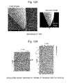
As shown in FIGS. 9 and 10 , from the locus of the first probe 5, the position of the tip of the second probe 6 was deduced as indicated by the dashed circle. The shape of the line connecting the points where the modulated signal was detected in the locus of the first probe 5 was similar to the profile of the tip of the second probe. In the verification experiment shown in FIGS. 9A and 9B , no damage was found at the tip of the first and second probes 5 and 6 after the experiment was finished. This indicates that the area near the second probe 6 was successfully scanned by the first probe 5 without a collision of the probes 5 and 6. In the verification experiment shown in FIGS. 10A and 10B , a gold coating was partially removed from the tip of the first and second probes 5 and 6 after the experiment was finished, although no damage was found in a glass portion. This suggests the possibility that the probes 5 and 6 came into contact with each other during the scanning by the first probe 5.
As is understood from FIG. 11B , when the distance between the probes 5 and 6 is not more than a certain value (i.e. when they are in proximity to each other), the modulated signal of the first probe 5 sharply attenuates. In addition, it has been found that the profile of the tip portion of the second probe 6 can be deduced from the shape of the modulated signal map of the first probe 5. After the experiment, a large detachment of the gold coating was found at the tip portion of the second probe 6 (refer to FIG. 11A ). However, the modulated signal map does not show an evidence of a collision of the two probes.
As shown in FIG. 12A , the tip portion of the two probes has a double-tapered shape, with two gradients extending at different angles. A two-stage gradient is also observed in the modulated map shown in FIG. 12B , which shows that it is possible to deduce the shape of the tip of a probe.
Next, the result of an observation of a carrier flow path will be described. The observation was performed for a single quantum well (SQW) sample of InGaN in the dual IC mode by using the aforementioned near-field optical microscope. In this experiment, the first probe 5 was used as the C probe and the second probe 6 as the I probe. The observation was performed while the first probe 5 was moved by the probe movement mechanism 10. The control of the distance between the first and second probes 5 and 6 was performed in the dualband modulation control method which was described earlier.
In particular, two lenses 101 and 102, and a mirror 103 are arranged on the emitted light path of an InGaN semiconductor laser 100. Five mirrors m1 through m5 and one beam splitter bs are arranged in a matrix pattern between the mirror 103 and three fiber mounts 104 through 106, as well as between the three fiber mounts 104 through 106 and a spectroscope 108. Each of the fiber mounts 104 through 106 holds an optical fiber having a probe at the end thereof. Each of the mirrors m1 through m5 and the beam splitter bs, which are arranged in a matrix pattern, can be moved to a position outside the optical path. A long path filter (LPF, 430 nm) 109 and a lens 110 are arranged between the spectroscope 108 and the mirror m5. The LPF 109 is used for cutting the excitation light of 405 nm emitted from the semiconductor laser 100. The light entering the spectroscope 108 through the LPF 109 and the lens 110 is detected by a liquid-nitrogen-cooled CCD 112.
Next, the second embodiment of the present invention will be described with reference to FIGS. 23 through 30 . The same components as in the first embodiment are indicated with the same numerals and the explanations of these components are omitted. The explanation will be made for the points which are different from the first embodiment.
The second embodiment is significantly different from the first embodiment in the following three points:
(1) the amplitude direction of the specific frequency and the arrangement of the crystal oscillators;
(2) the processing flow of the dualband modulation control method; and
(3) the method of probe scan.
In addition to the above, the present embodiment is different from the first embodiment in that the probes were coated with aluminum (Al), which is harder than gold (Au). However, the explanation for this regard is omitted and the aforementioned points (1) through (3) will be described one by one.
(1) Amplitude Direction of the Specific Frequency and the Arrangement of the Crystal Oscillators
In the present embodiment, such a design change can remove the mode in which the probes 5 and 6 tap the sample, preventing the tips of the probes 5 and 6 from touching the sample and being damaged.
(2) Processing Flow of the Dualband Modulation Control Method
In the present embodiment, tuning- fork crystal oscillators 25 and 27 having a resonant frequency around 32 kHz (32.7 kHz) are respectively attached to the first and second probes 5 and 6. The frequency (specific frequency) of the physical vibration provided to the first probe 5 was 100 Hz.
On the other hand, the use of the product of the signals of s3(x) of the probes 5 and 6 as in the present embodiment enables a signal detection by a kind of synchronous detection method, which improves the S/N ratio. This allows the threshold to be set at a low value so as to enhance the detection sensitivity.
Additionally, the use of the product of the signals of s3(x) of the probes 5 and 6 can prevent an erroneous determination that a change of the signal due to a pulse noise generated in one probe is mistaken for a change due to a proximity of the probes 5 and 6. In particular, since the change of the signals s3(x) are synchronized while the probes 5 and 6 are in proximity to each other, the use of the product of the signals of s3(x) of the probes 5 and 6 can eliminate an erroneous determination as much as possible while the probes 5 and 6 are distant from each other, allowing an accurate detection of the proximity of the probes 5 and 6.
(3) Method of Probe Scan
However, when the C probe is forced to move to the next line, the C probe and I probe might collide with each other due to this forced movement. In addition, when the C probe and I probe move closer to each other, not only the signal of the specific frequency (100 Hz), but also the signal of the resonant frequency (32 kHz) attenuates. Consequently, the control unit 22 erroneously determines that the C probe is moved to the sample, and moves the C probe to the direction away from the sample. As a result, in the reciprocating scanning method, the C probe moves away from the sample when the C probes performs a reciprocating scanning in the area where the C probe and the I probe are closest to each other.
Given this factor, in the second embodiment, a one-way scanning method as shown in FIG. 29 was used. FIG. 30 shows a sample surface image in the one-way scanning method. This method can avoid the collision of the probes 5 and 6 in performing a scanning in the area where the probes 5 and 6 are closest to each other. A comparison with FIG. 28 shows that, in the one-way scanning method, the difference in the color strength of the adjacent lines is small even in the area where the probes 5 and 6 are closest to each other, and the shade does not change within a line. This indicates that the C probe can be moved while maintaining a constant distance to the sample.
The present invention is not limited to the aforementioned embodiments, and a variety of changes are possible.
For example, the scanning probe microscope may be any type of microscope other than a scanning near-field optical microscope, such as a scanning tunnel microscope, an atomic force microscope, a magnetic force microscope, or a friction force microscope.
The number of the first and second probes is not limited to one. The number of both the first and second probes may be more than one. Or, the number of one probe may be one and that of the other probe may be more than one.
In the embodiments, the second probe was moved relative to the sample surface by moving the sample stage. However, the second probe may be directly moved to scan the sample surface. Such a directly moved probe may be either one of the first and second probes, or both the probes.
The vibration of the specific frequency may be provided to either the first probe or second probe. Alternatively, the vibration of the specific frequency may be provided to both probes.
The specific frequency is not limited to 100 Hz; it can be set at any value.
In the second embodiment, the proximity of the first and second probes was detected based on the product of the signals s3(x) regarding the distance between the first and second probes. However, the proximity of the probes can be detected based on the sum of the signals s3(x).
| EXPLANATION OF |
| 1 | Scanning Near- |
| 3 | |
| 5 | |
| 6 | |
| 8 | |
| 10 | |
| 12 | Distance Control Mechanism (Probe-Sample Distance Controller) |
| 14 | |
| 16 | |
| 22 | Control Unit (Controller, Vibrator, Probe Proximity Detector, and |
| Vibration Monitor) | |
| 25, 27 | |
| 29, 30 | |
| 32, 34 | Lock-In Amplifier (Vibration Monitor) |
Claims (20)
1. A scanning probe microscope having a first probe and a second probe both for scanning a sample while maintaining a constant distance to a surface of the sample, comprising:
a) a first scanner for moving the first probe relative to the sample;
b) a second scanner for moving the second probe relative to the sample;
c) a vibrator for providing either the first probe or the second probe with a vibration of a specific frequency;
d) a vibration monitor for monitoring the vibration of the specific frequency of the first probe and the second probe;
e) a probe proximity detector for detecting proximity of the first probe and the second probe to each other based on a change of at least either a vibration of the first probe or a vibration of the second probe; and
f) a controller for controlling the first scanner and the second scanner based on a result of detection by the probe proximity detector.
2. The scanning probe microscope according to claim 1 , wherein:
the vibrator provides the first probe with the vibration; and
the probe proximity detector detects proximity of the first probe and the second probe to each other based on a fact that a rate of change of the vibration of the first probe is equal to or less than a threshold.
3. The scanning probe microscope according to claim 1 , wherein:
the vibrator provides the first probe with the vibration; and
the probe proximity detector detects proximity of the first probe and the second probe to each other based on a fact that a rate of change of the vibration of the second probe exceeds a threshold.
4. The scanning probe microscope according to claim 3 , wherein the first probe and the second probe are attached to a first tuning-fork oscillator and a second tuning-fork oscillator, and the scanners move the first probe and the second probe while resonating the tuning-fork oscillators, and the scanning probe microscope comprising:
a voltage detector for detecting a voltage signal induced in each of the tuning-fork oscillators when a tip of the first probe and a tip of the second probe are individually approximated to the surface of the sample; and
a probe-sample distance controller for stabilizing a distance between the tip of each probe and the sample surface based on a result of detection by the voltage detector.
5. The scanning probe microscope according to claim 1 , wherein the first probe and the second probe are attached to a first tuning-fork oscillator and a second tuning-fork oscillator, and the scanners move the first probe and the second probe while resonating the tuning-fork oscillators, and the scanning probe microscope comprising:
a voltage detector for detecting a voltage signal induced in each of the tuning-fork oscillators when a tip of the first probe and a tip of the second probe are individually approximated to the surface of the sample; and
a probe-sample distance controller for stabilizing a distance between the tip of each probe and the sample surface based on a result of detection by the voltage detector.
6. The scanning probe microscope according to claim 2 , wherein:
the vibrator provides the first probe with the vibration; and
the probe proximity detector detects proximity of the first probe and the second probe to each other based on a fact that a rate of change of the vibration of the second probe exceeds a threshold.
7. The scanning probe microscope according to claim 2 , wherein the first probe and the second probe are attached to a first tuning-fork oscillator and a second tuning-fork oscillator, and the scanners move the first probe and the second probe while resonating the tuning-fork oscillators, and the scanning probe microscope comprising:
a voltage detector for detecting a voltage signal induced in each of the tuning-fork oscillators when a tip of the first probe and a tip of the second probe are individually approximated to the surface of the sample; and
a probe-sample distance controller for stabilizing a distance between the tip of each probe and the sample surface based on a result of detection by the voltage detector.
8. A scanning probe microscope having a first probe and a second probe both for scanning a sample while maintaining a constant distance to a surface of the sample, comprising:
a) a first tuning-fork oscillator to which the first probe is attached;
b) a second tuning-fork oscillator to which the second probe is attached;
c) a scanner for moving each of the first probe and the second probe relative to the sample while resonating each of the first tuning-fork oscillator and the second tuning-fork oscillator;
d) a vibrator for providing either the first probe or the second probe with a vibration of a specific frequency;
e) a signal detector for detecting a voltage signal of the specific frequency induced in each of the tuning-fork oscillators when the first probe and the second probe are approximated to each other while the first tuning-fork oscillator and the second tuning-fork oscillator are resonated; and
f) a probe proximity detector for detecting proximity of the first probe and the second probe to each other based on a voltage signal of the specific frequency induced in each of the first tuning-fork oscillator and the second tuning-fork oscillator.
9. The scanning probe microscope according to claim 8 , wherein:
the probe proximity detector detects proximity of the first probe and the second probe to each other based on a product of a voltage signal of the specific frequency induced in the first tuning-fork oscillator and a voltage signal of the specific frequency induced in the second tuning-fork oscillator.
10. The scanning probe microscope according to claim 9 , wherein:
the specific frequency is different from a resonance frequency of the tuning-fork oscillators.
11. The scanning probe microscope according to claim 8 , wherein:
the probe proximity detector detects proximity of the first probe and the second probe to each other based on a sum of a voltage signal of the specific frequency induced in the first tuning-fork oscillator and a voltage signal of the specific frequency induced in the second tuning-fork oscillator.
12. The scanning probe microscope according to claim 11 , wherein:
the specific frequency is different from a resonance frequency of the tuning-fork oscillators.
13. The scanning probe microscope according to claim 8 , wherein:
the specific frequency is different from a resonance frequency of the tuning-fork oscillators.
14. A method for detecting proximity of probes of a scanning probe microscope having a first probe and a second probe both for scanning a sample while maintaining a constant distance to a surface of the sample, comprising the steps of:
providing either the first probe or the second probe with a vibration of a specific frequency;
monitoring the vibration of the specific frequency of the first probe and the second probe; and
detecting proximity of the first probe and the second probe to each other based on a change of at least either a vibration of the specific frequency of the first probe or a vibration of the specific frequency of the second probe.
15. The method for detecting proximity of probes of a scanning probe microscope according to claim 14 , wherein:
the vibration of the specific frequency is provided to the first probe; and
proximity of the first probe and the second probe to each other is detected based on a fact that a rate of change of the vibration of the first probe is equal to or less than a threshold.
16. The method for detecting proximity of probes of a scanning probe microscope according to claim 15 , wherein:
the vibration of the specific frequency is provided to the first probe; and
proximity of the first probe and the second probe to each other is detected based on a fact that a rate of change of the vibration of the second probe exceeds a threshold.
17. The method for detecting proximity of probes of a scanning probe microscope according to claim 14 , wherein:
the vibration of the specific frequency is provided to the first probe; and
proximity of the first probe and the second probe to each other is detected based on a fact that a rate of change of the vibration of the second probe exceeds a threshold.
18. A method for detecting proximity of probes of a scanning probe microscope having a first probe and a second probe both for scanning a sample while maintaining a constant distance to a surface of the sample, wherein:
the first probe is attached to a first tuning-fork oscillator;
the second probe is attached to a second tuning-fork oscillator;
a vibration of a specific frequency is provided to either the first probe or the second probe; and
proximity of the first probe and the second probe to each other is detected based on a voltage signal of the specific frequency induced in each of the first tuning-fork oscillator and the second tuning-fork oscillator.
19. The method for detecting proximity of probes of a scanning probe microscope according to claim 18 , wherein:
proximity of the first probe and the second probe to each other is detected based on a product of a voltage signal of the specific frequency induced in the first tuning-fork oscillator and a voltage signal of the specific frequency induced in the second tuning-fork oscillator.
20. The method for detecting proximity of probes of a scanning probe microscope according to claim 18 , wherein:
proximity of the first probe and the second probe to each other is detected based on a sum of a voltage signal of the specific frequency induced in the first tuning-fork oscillator and a voltage signal of the specific frequency induced in the second tuning-fork oscillator.
Applications Claiming Priority (5)
| Application Number | Priority Date | Filing Date | Title |
|---|---|---|---|
| JP2009-149205 | 2009-06-23 | ||
| JP2009149205 | 2009-06-23 | ||
| JP2010025975 | 2010-02-08 | ||
| JP2010-025975 | 2010-02-08 | ||
| PCT/JP2010/060494 WO2010150756A1 (en) | 2009-06-23 | 2010-06-21 | Scanning probe microscope and probe proximity detection method therefor |
Publications (2)
| Publication Number | Publication Date |
|---|---|
| US20120124706A1 US20120124706A1 (en) | 2012-05-17 |
| US8479308B2 true US8479308B2 (en) | 2013-07-02 |
Family
ID=43386526
Family Applications (1)
| Application Number | Title | Priority Date | Filing Date |
|---|---|---|---|
| US13/380,261 Expired - Fee Related US8479308B2 (en) | 2009-06-23 | 2010-06-21 | Scanning probe microscope and method for detecting proximity of probes thereof |
Country Status (6)
| Country | Link |
|---|---|
| US (1) | US8479308B2 (en) |
| EP (1) | EP2447723A4 (en) |
| JP (1) | JP5733724B2 (en) |
| IL (1) | IL217151A0 (en) |
| RU (1) | RU2526295C2 (en) |
| WO (1) | WO2010150756A1 (en) |
Cited By (2)
| Publication number | Priority date | Publication date | Assignee | Title |
|---|---|---|---|---|
| WO2018063874A1 (en) * | 2016-09-28 | 2018-04-05 | Cascade Microtech, Inc. | Probe systems and methods |
| US11131699B2 (en) * | 2017-09-07 | 2021-09-28 | National Institute Of Advanced Science And Technology | Method for determining probe angle, high-frequency test system, program and storage medium |
Families Citing this family (1)
| Publication number | Priority date | Publication date | Assignee | Title |
|---|---|---|---|---|
| US20220299584A1 (en) * | 2021-03-11 | 2022-09-22 | Hi Llc | Devices, systems, and methods for suppressing optical noise in optically pumped magnetometers |
Citations (9)
| Publication number | Priority date | Publication date | Assignee | Title |
|---|---|---|---|---|
| US5214389A (en) * | 1992-01-06 | 1993-05-25 | Motorola, Inc. | Multi-dimensional high-resolution probe for semiconductor measurements including piezoelectric transducer arrangement for controlling probe position |
| US5721721A (en) * | 1987-08-25 | 1998-02-24 | Canon Kabushiki Kaisha | Two scanning probes information recording/reproducing system with one probe to detect atomic reference location on a recording medium |
| US5889208A (en) * | 1991-12-06 | 1999-03-30 | Canon Kabushiki Kaisha | Angular velocity sensor having cantilever beams |
| JP2002031591A (en) | 2000-07-17 | 2002-01-31 | Kansai Tlo Kk | Near-field optical microscope device |
| WO2004006302A2 (en) | 2002-07-08 | 2004-01-15 | Multiprobe, Inc. | Software synchronization of multiple scanning probes |
| US20050242283A1 (en) * | 2002-02-05 | 2005-11-03 | Tsuyoshi Hasegawa | Scanning probe microscope and specimen surface structure measuring method |
| JP2008014903A (en) | 2006-07-10 | 2008-01-24 | Hitachi High-Technologies Corp | Probe control apparatus |
| JP2008298487A (en) | 2007-05-29 | 2008-12-11 | Horiba Ltd | Scanning probe microscope and relative position measuring method of probes thereof |
| US7533561B2 (en) * | 2005-08-19 | 2009-05-19 | Arthur Beyder | Oscillator for atomic force microscope and other applications |
Family Cites Families (5)
| Publication number | Priority date | Publication date | Assignee | Title |
|---|---|---|---|---|
| JPH0989911A (en) * | 1995-09-22 | 1997-04-04 | Kared Karei & Mires Heines G Burgerrihen Rechts Mbh | Compound-oscillator scanning imager |
| US6028305A (en) * | 1998-03-25 | 2000-02-22 | Board Of Trustees Of The Leland Stanford Jr. University | Dual cantilever scanning probe microscope |
| JP4621908B2 (en) * | 2004-11-15 | 2011-02-02 | 国立大学法人京都大学 | Surface state measuring method, surface state measuring device, microscope, information processing device |
| JP2008089510A (en) * | 2006-10-04 | 2008-04-17 | Research Institute Of Biomolecule Metrology Co Ltd | Scanning probe microscope, probe for the same, and inspection method |
| JP4899162B2 (en) * | 2007-07-17 | 2012-03-21 | 独立行政法人産業技術総合研究所 | Scanning probe microscope probe and scanning probe microscope using the same |
-
2010
- 2010-06-21 WO PCT/JP2010/060494 patent/WO2010150756A1/en active Application Filing
- 2010-06-21 EP EP10792074.6A patent/EP2447723A4/en not_active Withdrawn
- 2010-06-21 US US13/380,261 patent/US8479308B2/en not_active Expired - Fee Related
- 2010-06-21 JP JP2011519892A patent/JP5733724B2/en active Active
- 2010-06-21 RU RU2012102057/28A patent/RU2526295C2/en not_active IP Right Cessation
-
2011
- 2011-12-22 IL IL217151A patent/IL217151A0/en unknown
Patent Citations (12)
| Publication number | Priority date | Publication date | Assignee | Title |
|---|---|---|---|---|
| US5721721A (en) * | 1987-08-25 | 1998-02-24 | Canon Kabushiki Kaisha | Two scanning probes information recording/reproducing system with one probe to detect atomic reference location on a recording medium |
| US5889208A (en) * | 1991-12-06 | 1999-03-30 | Canon Kabushiki Kaisha | Angular velocity sensor having cantilever beams |
| US5214389A (en) * | 1992-01-06 | 1993-05-25 | Motorola, Inc. | Multi-dimensional high-resolution probe for semiconductor measurements including piezoelectric transducer arrangement for controlling probe position |
| JP2002031591A (en) | 2000-07-17 | 2002-01-31 | Kansai Tlo Kk | Near-field optical microscope device |
| US20050242283A1 (en) * | 2002-02-05 | 2005-11-03 | Tsuyoshi Hasegawa | Scanning probe microscope and specimen surface structure measuring method |
| WO2004006302A2 (en) | 2002-07-08 | 2004-01-15 | Multiprobe, Inc. | Software synchronization of multiple scanning probes |
| US20040025578A1 (en) | 2002-07-08 | 2004-02-12 | Hare Casey Patrick | Software synchronization of multiple scanning probes |
| CN1666312A (en) | 2002-07-08 | 2005-09-07 | 马尔蒂普罗布公司 | Software synchronization of multiple scanning probes |
| JP2005532555A (en) | 2002-07-08 | 2005-10-27 | マルチプローブ・インコーポレーテッド | Software synchronization of multiple scanning probes |
| US7533561B2 (en) * | 2005-08-19 | 2009-05-19 | Arthur Beyder | Oscillator for atomic force microscope and other applications |
| JP2008014903A (en) | 2006-07-10 | 2008-01-24 | Hitachi High-Technologies Corp | Probe control apparatus |
| JP2008298487A (en) | 2007-05-29 | 2008-12-11 | Horiba Ltd | Scanning probe microscope and relative position measuring method of probes thereof |
Non-Patent Citations (4)
| Title |
|---|
| International Preliminary Report on Patentability issued in Application No. PCT/JP2010/060494; Dated Jan. 17, 2012 (With Translation). |
| International Search Report issued in Application No. PCT/JP2010/060494; Dated Sep. 7, 2010 (With Translation). |
| Micheletto et al., "Direct mapping of the far and near filed optical emission of nano-sized tapered glass fibers by an integrated SNOM/SF system," Applied Surface Science, vol. 144-145, pp. 514-519, Apr. 1999. |
| Sigehuzi et al., "Dual-probe Scanning Near-field Optical Microscope," Technical Report of IEICE, OME Dec. 1996 (May 1996), pp. 13-18, (With English-language Abstract). |
Cited By (4)
| Publication number | Priority date | Publication date | Assignee | Title |
|---|---|---|---|---|
| WO2018063874A1 (en) * | 2016-09-28 | 2018-04-05 | Cascade Microtech, Inc. | Probe systems and methods |
| US10459006B2 (en) | 2016-09-28 | 2019-10-29 | Formfactor Beaverton, Inc. | Probe systems and methods |
| US11047879B2 (en) | 2016-09-28 | 2021-06-29 | Formfactor, Inc. | Probe systems and methods |
| US11131699B2 (en) * | 2017-09-07 | 2021-09-28 | National Institute Of Advanced Science And Technology | Method for determining probe angle, high-frequency test system, program and storage medium |
Also Published As
| Publication number | Publication date |
|---|---|
| RU2012102057A (en) | 2013-07-27 |
| US20120124706A1 (en) | 2012-05-17 |
| JP5733724B2 (en) | 2015-06-10 |
| EP2447723A1 (en) | 2012-05-02 |
| IL217151A0 (en) | 2012-02-29 |
| RU2526295C2 (en) | 2014-08-20 |
| JPWO2010150756A1 (en) | 2012-12-10 |
| WO2010150756A1 (en) | 2010-12-29 |
| EP2447723A4 (en) | 2014-01-15 |
Similar Documents
| Publication | Publication Date | Title |
|---|---|---|
| EP0674200B1 (en) | Scanning near-field optic/atomic force microscope | |
| JP4496350B2 (en) | Atomic force microscope | |
| JPH0650750A (en) | Scanning-type microscope including force detecting means | |
| US6983644B2 (en) | Specimen observation method in atomic force microscopy and atomic force microscope | |
| US20100207039A1 (en) | Probe Microscopy and Probe Position Monitoring Apparatus | |
| JP4851375B2 (en) | Phase feedback AFM control method and phase feedback AFM | |
| US8479308B2 (en) | Scanning probe microscope and method for detecting proximity of probes thereof | |
| JPH11160333A (en) | Scanning probe microscope | |
| JP4474556B2 (en) | Scanning probe microscope | |
| JP4913242B2 (en) | Dynamic mode AFM device | |
| JP2008544270A (en) | Higher order harmonic atomic force microscope | |
| JP2000146804A (en) | Method for determining distance between near-field probe and sample surface to be inspected and near-field microscope | |
| JP2005274495A (en) | High frequency minute vibration measuring apparatus | |
| JP2000039390A (en) | Non-contact atomic force microscope | |
| JP2006215004A (en) | Near-field optical microscope and method for measuring sample by using near-field light | |
| WO2010067570A1 (en) | Method for processing output of scanning type probe microscope, and scanning type probe microscope | |
| JP4361221B2 (en) | Measurement method of illumination reflection mode in scanning near-field microscope | |
| JP3935350B2 (en) | Distance control method and scanning probe microscope using the same | |
| JPH09178761A (en) | Probe contact monitor for ac mode scanning probe microscope | |
| JP2004101378A (en) | Near-field scanning optical microscopy and method for observing sample using nearfield light | |
| CN111630396B (en) | Scanning probe microscope and analysis method | |
| JPH1151863A (en) | Method for measuring index of refraction and microscopic surface observation device | |
| JP2006275875A (en) | Scanning probe microscope | |
| JP2001059807A (en) | Method and apparatus for processing probe | |
| JP2014199689A (en) | Magnetic head inspection device and magnetic head inspection method |
Legal Events
| Date | Code | Title | Description |
|---|---|---|---|
| AS | Assignment |
Owner name: KYOTO UNIVERSITY, JAPAN Free format text: ASSIGNMENT OF ASSIGNORS INTEREST;ASSIGNORS:NISHIMURA, KATSUHITO;KAWAKAMI, YOICHI;FUNATO, MITSURU;AND OTHERS;SIGNING DATES FROM 20111206 TO 20111218;REEL/FRAME:027597/0572 |
|
| REMI | Maintenance fee reminder mailed | ||
| LAPS | Lapse for failure to pay maintenance fees | ||
| STCH | Information on status: patent discontinuation |
Free format text: PATENT EXPIRED DUE TO NONPAYMENT OF MAINTENANCE FEES UNDER 37 CFR 1.362 |
|
| FP | Lapsed due to failure to pay maintenance fee |
Effective date: 20170702 |