EP1519304B1 - Firmware update using a dedicated cable - Google Patents
Firmware update using a dedicated cable Download PDFInfo
- Publication number
- EP1519304B1 EP1519304B1 EP04023057A EP04023057A EP1519304B1 EP 1519304 B1 EP1519304 B1 EP 1519304B1 EP 04023057 A EP04023057 A EP 04023057A EP 04023057 A EP04023057 A EP 04023057A EP 1519304 B1 EP1519304 B1 EP 1519304B1
- Authority
- EP
- European Patent Office
- Prior art keywords
- cable
- printing apparatus
- connector
- data
- dedicated
- Prior art date
- Legal status (The legal status is an assumption and is not a legal conclusion. Google has not performed a legal analysis and makes no representation as to the accuracy of the status listed.)
- Not-in-force
Links
Images


Classifications
-
- G—PHYSICS
- G06—COMPUTING; CALCULATING OR COUNTING
- G06K—GRAPHICAL DATA READING; PRESENTATION OF DATA; RECORD CARRIERS; HANDLING RECORD CARRIERS
- G06K15/00—Arrangements for producing a permanent visual presentation of the output data, e.g. computer output printers
-
- G—PHYSICS
- G06—COMPUTING; CALCULATING OR COUNTING
- G06F—ELECTRIC DIGITAL DATA PROCESSING
- G06F8/00—Arrangements for software engineering
- G06F8/60—Software deployment
- G06F8/65—Updates
-
- G—PHYSICS
- G06—COMPUTING; CALCULATING OR COUNTING
- G06K—GRAPHICAL DATA READING; PRESENTATION OF DATA; RECORD CARRIERS; HANDLING RECORD CARRIERS
- G06K15/00—Arrangements for producing a permanent visual presentation of the output data, e.g. computer output printers
- G06K15/02—Arrangements for producing a permanent visual presentation of the output data, e.g. computer output printers using printers
- G06K15/18—Conditioning data for presenting it to the physical printing elements
- G06K15/1801—Input data handling means
- G06K15/1803—Receiving particular commands
Definitions
- the present invention relates to an electronic apparatus including a computer, such, for example, as a printer.
- an electronic apparatus including a computer such as, for example, a printer
- its program and data used by the included computer are stored in an unrewritable ROM or in a rewritable nonvolatile memory (for example, a flash memory, EEPROM or the like).
- a rewritable nonvolatile memory for example, a flash memory, EEPROM or the like.
- JP 1-112424 A discloses a method for updating the version of an incorporated program by transmitting a file from a host computer to a laser printer, determining whether or not the file data is a program present in the laser printer that receives the file, and if the file is a new program, storing it in a program area of its nonvolatile memory and executing it when desired.
- Document EP 0583077 A1 discloses a pair of mobile communications handset terminals.
- a cable loom comprises a link, which has a further link line that connects an input terminal of one the handset terminals with an output terminal thereof. The presence of this link line leads to a changed voltage supply on two separate line connected to an AD converter which may thus detect the insertion of the cable loom.
- a microprocessor closes a switch thereby increasing the voltage supply to a non-volatile memory such that a reprogramming mode can be entered.
- Document JP 2002-166628 A1 discloses an inkjet printer, wherein its firmware stored in an EEPROM may be updated by providing a cartridge having a memory, in which the update is stored. Via an interface to the memory, the update is allowed to be written into the EEPROM after performing various judgment, version and support checks.
- the present invention has been made to address a problem that it is difficult to rewrite a program or data used by a computer incorporated in an electronic apparatus such as a printer. Accordingly, one object of the present invention is to provide an electronic apparatus in which changing over to a specific mode such as a mode for transmitting the program or data is enabled without carrying out any special work or control.
- one aspect of the present invention provides a printing apparatus according to claim 1 and a method of controlling the same according to claim 12.
- the printing apparatus includes a memory medium that stores a rewritable control program
- the predetermined mode may be a mode for rewriting the control program or data stored in the memory medium.
- the rewritable control program or data may be firmware for the printing apparatus.
- the firmware that is stored in the internal memory medium of the printing apparatus may include both a control program and data to control the printing apparatus.
- the printing apparatus of aspects of the present invention automatically changes the mode if it is determined that the cable connected to the connector is a dedicated cable, no special control for determining the kind of data transmitted through the cable is necessary.
- the printing apparatus can determine that it is the dedicated cable simply by connecting the cable to the connector.
- the interface connector used ordinarily for connecting to an external apparatus may be used as a connector on which to connect the dedicated cable. Consequently, the mode selection can be carried out easily using an existing connector without preparing any special connector.
- the connector on which the dedicated cable is loaded may be provided on a substrate inside the printing apparatus. Consequently, the structure of the connector can be designed freely by preparing a connector on which a dedicated cable for mode selection is to be loaded.
- the connector used ordinarily for transmitting print data can be used as a connector to which the dedicated cable is connected, thereby necessitating no special reconstruction or the like of the printing apparatus.
- the operation mode of the printing apparatus can be changed to a dedicated mode for rewriting the control program or data by connecting the dedicated cable to the connector.
- the dedicated mode By preparing the dedicated mode, the control program or data can be rewritten without any special control for determining the type of data to be input from the connector.
- the operation mode can be changed to the dedicated mode simply by connecting the dedicated cable to the connector, even an inexperienced user can execute the re-programming operation with few mistakes.
- this is a dedicated mode even if a fault occurs during reception of the control program or data, it is possible to construct so as to enable rewriting of the control program or data without affecting other controls.
- the operation mode of the printing apparatus is changed to the dedicated mode for rewriting the firmware by connecting the dedicated cable to the connector, the firmware can be rewritten easily. Consequently, no troublesome operation for changing the operation mode to the firmware rewriting dedicated mode is required, so that the newest firmware can be used easily.
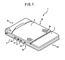
- FIG. 1 is a perspective view showing the appearance of a printing apparatus implementing aspects of the invention
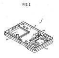
- FIG. 2 is a perspective view showing a state in which the rear face cover of the FIG. 1 printing apparatus is removed as seen from the rear side;
- FIG. 3 is a block diagram showing the electrical structure of the FIG. 1 printing apparatus
- FIG. 4 is a front view of a face of a dedicated cable to be connected to a serial connector of the FIG. 1 printing apparatus;
- FIG. 5 is a connection diagram of terminals of the special cable that is usable with the invention.
- FIG. 6 is a flow chart showing the flow of mode changeover processing according to aspects of the invention.
- FIG. 1 is a perspective view showing the appearance of the printing apparatus 1.
- FIG. 2 is a perspective view showing a state in which the rear face cover of the printing apparatus 1 is removed as seen from the rear side.
- the main body case 2 of the printing apparatus 1 is substantially rectangular in its plan view, more specifically a substantially A6 size shape having a length of about 16 cm and a width of about 10 cm and a rectangular solid having a depth of about 2 cm.
- the main body case 2 has case side faces 2a, 2b, 2c, and 2d and various kinds of interfaces are disposed along the length direction of the case side face 2a.
- An AC adaptor connector 62 for receiving power, a serial connector 21 for executing serial communication with an external apparatus, a USB connector 31 for communicating with an external apparatus based on the USB standard, and a power switch 66 for turning ON/OFF the power of the printing apparatus 1 are provided on the case side face 2a in this order from the right side thereof.
- a substantially rectangular fixed cover 3 is provided on the top face near an end in the length direction of the main body case 2, occupying about 1/4 area in the top face of the main body.
- a printing mechanism portion having a paper feed roller for feeding paper (not shown), a thermal head 18 (see FIG. 3 ) which prints by heating and the like is provided inside the portion of the main body case 2 covered with the fixed cover 3.
- An accommodation portion (not shown) which accommodates paper to be printed is provided in a portion other than the portion under the fixed cover 3 of the top face of the main body case 2, and is covered with a case cover 4.
- a discharge port 28 for discharging a printed paper from the printing mechanism portion is provided between the fixed cover 3 and the case cover 4.
- a control circuit board 6 (main substrate) having a CPU 10 (see FIG. 3 ) for controlling the printing apparatus 1, an internal connector 40 for transmitting/receiving print data, a DRAM 13, a FROM 12, an EEPROM 11 (see FIG. 3 ) and other various circuits, and a battery 30 for supplying power to the printing apparatus 1 are provided below the accommodation portion.
- the rear face of the main body case 2 is covered with a rear face cover (not shown), and by removing the rear face cover, the control circuit board 6, the internal connector 40 and a flat cable 41 can be accessed.
- the flat cable 41 is for transmitting print data from the CPU 10 to a thermal head 18, and is mounted to the internal connector 40.
- the printing apparatus 1 utilizes the thermal head 18 as its printing head and thermal paper as a printing medium.
- the reason why the thermal head 18 is utilized as the printing head is that no reciprocating mechanism is required, unlike most ink jet type or ink ribbon type printing heads, thereby achieving reduction in size. Further, its economic efficiency is excellent because the only required consumption good is paper.
- As the thermal paper a thermal color development type, which has a color development layer in which dye and developer chemically combine with each other when heated by the thermal head to develop a color, a thermal boring type in which a boring layer which is bored by heating is formed on a base layer thereof and the like are available.
- the invention is applicable to other types of printers such as, for example, the above-noted ink jet printers, laser printers, etc.
- FIG. 3 is a block diagram showing the electrical structure of the printing apparatus 1.
- the EEPROM 11, FROM 12, and DRAM 13 are connected to the CPU 10 that controls the printing apparatus 1.
- the EEPROM 11 stores model information, production number, count information of print number, and maintenance information such as information specific to an individual printing apparatus 1.
- the FROM 12 stores control programs and data used for printing such as character data and graphic data, and if the operation mode is changed to rewrite mode by connecting a dedicated cable 42, as described later, the contents of the control program and data stored in the FROM 12 can be rewritten. Further, data values which occur during arithmetic operations are stored temporarily in the DRAM 13.
- the printing mechanism portion of the printing apparatus 1 includes a step motor 17 that feeds paper, a thermal head 18 that prints by heating, a feed motor drive circuit 14 that drives the step motor 17 and a thermal head control circuit 15 that controls the thermal head 18.
- the thermal head control circuit 15 and the feed motor drive circuit 14 are driven according to an instruction from the CPU 10 to execute printing.
- a cassette sensor 24 that detects whether or not a paper cassette (not shown) is loaded
- a paper detection sensor 22 that detects whether or not a thermal paper is located at printing position
- a head temperature detecting circuit 23 that detects the temperature of the thermal head 18
- an IrDA circuit 25 a USB interface circuit 26 that achieves USB connection
- a serial interface circuit 27 that executes serial connection are connected to the CPU 10 to execute communication with external apparatus through these components.
- a mode indication LED 29 is connected to the CPU 10 to indicate the mode of the printing apparatus 1 (e.g., printing, data writing, program rewriting, and the like) through an indication state or color, for example.
- the printing apparatus 1 contains a battery 30 composed of a lithium ion battery which is rechargeable by a charging circuit 32 when connected to an AC adaptor 31, and this battery 30 supplies the printing apparatus 1 with power.
- the battery 30 is connected to the thermal head control circuit 15 and to the motor drive circuit 14 to supply power to these circuits, and further is connected to a three-terminal regulator 33.
- the voltage is regulated to 5V by the three-terminal regulator 33 and then supplied to the CPU 10.
- the apparatus also could use a non-rechargeable battery.
- FIG. 4 is a front view of a face of a dedicated cable 42 to be connected to a serial connector 21.
- FIG. 5 is a schematic diagram showing a connection diagram of terminals 43 of the dedicated cable 42. In FIG. 5 , the right side indicates the side of the dedicated cable 42 and the left side indicates the side of the serial connector 21.
- the dedicated cable 42 to be connected to the serial connector 21 is similar to a general purpose serial cable for transmitting print data from an external apparatus such as, for example, a personal computer, or any other portable information terminal, to the printing apparatus 1.
- the serial connector 21 has eight terminals for transmitting/receiving signals
- the dedicated cable 42 has eight terminals 43 corresponding to these terminals just like a general purpose serial cable.
- the terminals No. 2 - No.7 are used for transmitting/ receiving data.
- the remaining two terminals are not used for transmitting/receiving ordinary data, and remain as empty terminals.
- One of them is connected to the CPU 10 within the printing apparatus 1 (terminal No. 8 in FIG. 5 ) while the other is grounded (terminal No. 1 in FIG. 5 ).
- the terminals No. 1 and No. 8 are not grounded when the ordinarily used general purpose serial cable is connected to the serial connector 21, a high level signal is input to the CPU 10.
- the terminals No. 1 and No. 8 can be considered to be redundant terminals because they are not used under normal conditions. These terminals also are not used for the transmission of data.
- terminals No. 1 and No. 8 are connected to each other in the dedicated cable 42.
- the terminal No. 8 of the serial connector 21 is connected to the CPU 10 and the terminal No. 1 is grounded to 0V, so that 0V signal, that is, a low level signal is input into the CPU 10 through the terminal No. 8 from the terminal No. 1.
- the dedicated cable 42 is so connected, the low level signal is input to the CPU 10, unlike when the ordinary general purpose cable is connected, so that the CPU 10 is capable of recognizing immediately that the dedicated cable 42 is connected. Therefore, mode selection is enabled according to a signal input from the terminal No. 8 of the serial connector 21.
- the terminal No. 8 of the serial connector 21 will be called the mode selection terminal.
- FIG. 6 is a flow chart showing the flow of mode selection processing. If, as shown in FIG. 6 , the power switch is turned ON (S10), it is determined whether or not the high level signal is input to the mode selection terminal (terminal No. 8 in FIG. 5 ) (S20). If the high level signal is input to the mode selection terminal (S20: YES), it can be determined that the terminals No. 1 and No. 8 are connected with an ordinary cable and therefore printing is executed according to ordinary connecting action.
- the mode selection terminal S20: NO
- the appropriate terminal of the serial connector 21 is connected to the mode selection terminal within the cable, and therefore it can be determined that a dedicated cable having a structure according to this embodiment of the invention is connected.
- the mode is changed to program rewrite mode (S30) and the mode selection LED is lit in red (S40).
- a control program such as, for example, firmware or data such as character data and graphic data are received from an external apparatus (S50), and if the reception ends, that program or data is transmitted to the CPU 10 and written into the internal RAM of the CPU 10 (S60).
- the newly downloaded program or data stored in the internal RAM is written into the FROM 12 (S70) and then the processing ends.
- the dedicated cable 42 is connected to the printing apparatus 1, and the printing apparatus 1 is powered ON, the low level signal is input to the CPU 10. Because usually the high level signal is input to this mode selection terminal, the CPU can determine immediately that the dedicated cable 42 is connected. Therefore, just after the cable is connected, it is possible to change the mode and execute download of data and/or program. Therefore, no special control of determining the kind of transmitted data and distinguishing from an ordinary action, such as reception of print data, is required.
- the mode selection is automatically carried out if the dedicated cable 42 is connected, even if any fault such as an operation interruption occurs during downloading of data and/or program, only a sequence of operations, namely, reception and write of data and/or program from the downloading, needs to be re-executed. Consequently, it is possible to avoid such a fault that normal version updating or reset is disabled as a result of a stoppage of the electronic apparatus during rewriting of the firmware.
- the CPU 10 which determines whether or not an input signal to the mode selection terminal is high functions as determining means, and the CPU 10 which executes the mode selection processing in S30 functions as mode selection means.
- the dedicated cable 42 to be connected to the serial connector 21 is used as the dedicated cable
- the dedicated cable is not restricted to a serial cable. Rather, any kind of cable may be used as long as it has terminals usable for mode selection.
- the flat cable 41 and the internal connector 40 connecting the thermal head 18, which can be accessed when the rear face of the printing apparatus 1 is opened are dedicated components of the printing apparatus 1 as shown in FIG. 2 , they can be provided with dedicated terminals for mode selection.
- the controller (CPU 10) preferably is implemented using a suitably programmed general purpose computer, e.g., a microprocessor, microcontroller or other processor device (CPU or MPU). It will be appreciated by those skilled in the art, that the controller also can be implemented as a single special purpose integrated circuit (e.g., ASIC) having a main or central processor section for overall, system-level control, and separate sections dedicated to performing various different specific computations, functions and other processes under control of the central processor section.
- ASIC application specific integrated circuit
- the controller also can be implemented using a plurality of separate dedicated or programmable integrated or other electronic circuits or devices (e.g., hardwired electronic or logic circuits such as discrete element circuits, or programmable logic devices such as PLDs, PLAs, PALs or the like).
- the controller also can be implemented using a suitably programmed general purpose computer in conjunction with one or more peripheral (e.g., integrated circuit) data and signal processing devices.
- peripheral e.g., integrated circuit
Applications Claiming Priority (2)
| Application Number | Priority Date | Filing Date | Title |
|---|---|---|---|
| JP2003336988 | 2003-09-29 | ||
| JP2003336988A JP2005103789A (ja) | 2003-09-29 | 2003-09-29 | 電子機器 |
Publications (2)
| Publication Number | Publication Date |
|---|---|
| EP1519304A1 EP1519304A1 (en) | 2005-03-30 |
| EP1519304B1 true EP1519304B1 (en) | 2010-08-25 |
Family
ID=34191549
Family Applications (1)
| Application Number | Title | Priority Date | Filing Date |
|---|---|---|---|
| EP04023057A Not-in-force EP1519304B1 (en) | 2003-09-29 | 2004-09-28 | Firmware update using a dedicated cable |
Country Status (5)
| Country | Link |
|---|---|
| US (1) | US20050068575A1 (ja) |
| EP (1) | EP1519304B1 (ja) |
| JP (1) | JP2005103789A (ja) |
| AT (1) | ATE479160T1 (ja) |
| DE (1) | DE602004028785D1 (ja) |
Cited By (1)
| Publication number | Priority date | Publication date | Assignee | Title |
|---|---|---|---|---|
| US10067751B2 (en) | 2009-02-27 | 2018-09-04 | Sagemcom Broadband Sas | Method of diagnosing and/or updating of software of an electronic device equipped with an HDMI type connector and associated device |
Families Citing this family (3)
| Publication number | Priority date | Publication date | Assignee | Title |
|---|---|---|---|---|
| KR100804647B1 (ko) * | 2005-11-15 | 2008-02-20 | 삼성전자주식회사 | 병렬형 플래시 인터페이스를 지원하는 직렬형 플래시메모리 장치를 이용한 시스템 부팅 방법 및 장치 |
| JP6309712B2 (ja) * | 2013-03-26 | 2018-04-11 | サトーホールディングス株式会社 | プリンタ |
| JP5856705B2 (ja) * | 2015-03-12 | 2016-02-10 | Kyb株式会社 | 作業機の制御装置 |
Family Cites Families (3)
| Publication number | Priority date | Publication date | Assignee | Title |
|---|---|---|---|---|
| GB2269032B (en) * | 1992-07-21 | 1996-03-20 | Orbitel Mobile Communications | Reprogramming methods and apparatus |
| JP3491419B2 (ja) * | 1995-12-04 | 2004-01-26 | 株式会社デンソー | 電子制御装置 |
| JP2002166628A (ja) * | 2000-12-01 | 2002-06-11 | Seiko Epson Corp | 着色媒体カートリッジ、プリンタ、プリントシステム、ファームウェアのアップデートシステム、およびプリンタドライバのアップデートシステム |
-
2003
- 2003-09-29 JP JP2003336988A patent/JP2005103789A/ja active Pending
-
2004
- 2004-08-17 US US10/919,388 patent/US20050068575A1/en not_active Abandoned
- 2004-09-28 AT AT04023057T patent/ATE479160T1/de not_active IP Right Cessation
- 2004-09-28 DE DE602004028785T patent/DE602004028785D1/de active Active
- 2004-09-28 EP EP04023057A patent/EP1519304B1/en not_active Not-in-force
Cited By (1)
| Publication number | Priority date | Publication date | Assignee | Title |
|---|---|---|---|---|
| US10067751B2 (en) | 2009-02-27 | 2018-09-04 | Sagemcom Broadband Sas | Method of diagnosing and/or updating of software of an electronic device equipped with an HDMI type connector and associated device |
Also Published As
| Publication number | Publication date |
|---|---|
| ATE479160T1 (de) | 2010-09-15 |
| US20050068575A1 (en) | 2005-03-31 |
| EP1519304A1 (en) | 2005-03-30 |
| JP2005103789A (ja) | 2005-04-21 |
| DE602004028785D1 (de) | 2010-10-07 |
Similar Documents
| Publication | Publication Date | Title |
|---|---|---|
| RU2333837C2 (ru) | Картридж и записывающее устройство | |
| EP1717041B1 (en) | Access to printing material container | |
| JP4047328B2 (ja) | 液体収納容器、該容器を用いる液体供給システムおよび記録装置、並びに前記容器用回路基板 | |
| US8291154B2 (en) | Memory device accepting write data and inverted write data from a host circuit | |
| EP1658976A1 (en) | Ink jet recording apparatus, semiconductor device, and recording head apparatus | |
| US20090237439A1 (en) | Mountable apparatus, board, and method of rewriting liquid information | |
| JPH11314377A (ja) | 交換可能なプリント部品のための電気的な記憶装置 | |
| JP2004098564A (ja) | 使用済みインクカートリッジのための再利用化用具 | |
| EP1519304B1 (en) | Firmware update using a dedicated cable | |
| CN113352770B (zh) | 耗材芯片及成像盒 | |
| JPH0661971B2 (ja) | プリンタ | |
| JP2001022571A (ja) | 電子機器及び該電子機器の制御プログラム書き換え方法 | |
| JP2009190408A (ja) | カートリッジ | |
| JP4075943B2 (ja) | プリンタ、プリンタシステム及びプリンタにおけるエラー検出方法 | |
| JP3720652B2 (ja) | ダウンロード方法及びこのダウンロード方法に用いられるポータブルプリンタ | |
| JP2004188634A (ja) | 印刷装置およびインクタンクおよび情報収集方法 | |
| JP4193002B2 (ja) | プリンタ、及びプリンタにおけるエラーチェック方法 | |
| JPH08212079A (ja) | 画像形成装置 | |
| JP2004348457A (ja) | 交換可能に取り付けられる部品及び製品 | |
| JPH07314798A (ja) | プリンタ装置 | |
| JP2000334999A (ja) | 光プリントヘッド | |
| JP2005149211A (ja) | データ記録装置およびデータ書き換え方法 | |
| JPH11175286A (ja) | 印刷制御システム及び方法、記憶媒体 | |
| JP2001058449A (ja) | プリンタ | |
| JPH0825773A (ja) | インパクトプリンタの寿命検出方式 |
Legal Events
| Date | Code | Title | Description |
|---|---|---|---|
| PUAI | Public reference made under article 153(3) epc to a published international application that has entered the european phase |
Free format text: ORIGINAL CODE: 0009012 |
|
| AK | Designated contracting states |
Kind code of ref document: A1 Designated state(s): AT BE BG CH CY CZ DE DK EE ES FI FR GB GR HU IE IT LI LU MC NL PL PT RO SE SI SK TR |
|
| AX | Request for extension of the european patent |
Extension state: AL HR LT LV MK |
|
| 17P | Request for examination filed |
Effective date: 20050304 |
|
| AKX | Designation fees paid |
Designated state(s): AT BE BG CH CY CZ DE DK EE ES FI FR GB GR HU IE IT LI LU MC NL PL PT RO SE SI SK TR |
|
| 17Q | First examination report despatched |
Effective date: 20060904 |
|
| GRAP | Despatch of communication of intention to grant a patent |
Free format text: ORIGINAL CODE: EPIDOSNIGR1 |
|
| GRAS | Grant fee paid |
Free format text: ORIGINAL CODE: EPIDOSNIGR3 |
|
| GRAA | (expected) grant |
Free format text: ORIGINAL CODE: 0009210 |
|
| AK | Designated contracting states |
Kind code of ref document: B1 Designated state(s): AT BE BG CH CY CZ DE DK EE ES FI FR GB GR HU IE IT LI LU MC NL PL PT RO SE SI SK TR |
|
| REG | Reference to a national code |
Ref country code: GB Ref legal event code: FG4D |
|
| REG | Reference to a national code |
Ref country code: CH Ref legal event code: EP |
|
| REG | Reference to a national code |
Ref country code: IE Ref legal event code: FG4D |
|
| REF | Corresponds to: |
Ref document number: 602004028785 Country of ref document: DE Date of ref document: 20101007 Kind code of ref document: P |
|
| REG | Reference to a national code |
Ref country code: NL Ref legal event code: VDEP Effective date: 20100825 |
|
| PG25 | Lapsed in a contracting state [announced via postgrant information from national office to epo] |
Ref country code: FI Free format text: LAPSE BECAUSE OF FAILURE TO SUBMIT A TRANSLATION OF THE DESCRIPTION OR TO PAY THE FEE WITHIN THE PRESCRIBED TIME-LIMIT Effective date: 20100825 Ref country code: AT Free format text: LAPSE BECAUSE OF FAILURE TO SUBMIT A TRANSLATION OF THE DESCRIPTION OR TO PAY THE FEE WITHIN THE PRESCRIBED TIME-LIMIT Effective date: 20100825 |
|
| PG25 | Lapsed in a contracting state [announced via postgrant information from national office to epo] |
Ref country code: PL Free format text: LAPSE BECAUSE OF FAILURE TO SUBMIT A TRANSLATION OF THE DESCRIPTION OR TO PAY THE FEE WITHIN THE PRESCRIBED TIME-LIMIT Effective date: 20100825 Ref country code: SI Free format text: LAPSE BECAUSE OF FAILURE TO SUBMIT A TRANSLATION OF THE DESCRIPTION OR TO PAY THE FEE WITHIN THE PRESCRIBED TIME-LIMIT Effective date: 20100825 Ref country code: CY Free format text: LAPSE BECAUSE OF FAILURE TO SUBMIT A TRANSLATION OF THE DESCRIPTION OR TO PAY THE FEE WITHIN THE PRESCRIBED TIME-LIMIT Effective date: 20100825 Ref country code: PT Free format text: LAPSE BECAUSE OF FAILURE TO SUBMIT A TRANSLATION OF THE DESCRIPTION OR TO PAY THE FEE WITHIN THE PRESCRIBED TIME-LIMIT Effective date: 20101227 Ref country code: BG Free format text: LAPSE BECAUSE OF FAILURE TO SUBMIT A TRANSLATION OF THE DESCRIPTION OR TO PAY THE FEE WITHIN THE PRESCRIBED TIME-LIMIT Effective date: 20101125 |
|
| PG25 | Lapsed in a contracting state [announced via postgrant information from national office to epo] |
Ref country code: NL Free format text: LAPSE BECAUSE OF FAILURE TO SUBMIT A TRANSLATION OF THE DESCRIPTION OR TO PAY THE FEE WITHIN THE PRESCRIBED TIME-LIMIT Effective date: 20100825 Ref country code: SE Free format text: LAPSE BECAUSE OF FAILURE TO SUBMIT A TRANSLATION OF THE DESCRIPTION OR TO PAY THE FEE WITHIN THE PRESCRIBED TIME-LIMIT Effective date: 20100825 Ref country code: BE Free format text: LAPSE BECAUSE OF FAILURE TO SUBMIT A TRANSLATION OF THE DESCRIPTION OR TO PAY THE FEE WITHIN THE PRESCRIBED TIME-LIMIT Effective date: 20100825 Ref country code: GR Free format text: LAPSE BECAUSE OF FAILURE TO SUBMIT A TRANSLATION OF THE DESCRIPTION OR TO PAY THE FEE WITHIN THE PRESCRIBED TIME-LIMIT Effective date: 20101126 |
|
| PG25 | Lapsed in a contracting state [announced via postgrant information from national office to epo] |
Ref country code: MC Free format text: LAPSE BECAUSE OF NON-PAYMENT OF DUE FEES Effective date: 20100930 Ref country code: DK Free format text: LAPSE BECAUSE OF FAILURE TO SUBMIT A TRANSLATION OF THE DESCRIPTION OR TO PAY THE FEE WITHIN THE PRESCRIBED TIME-LIMIT Effective date: 20100825 |
|
| REG | Reference to a national code |
Ref country code: CH Ref legal event code: PL |
|
| PG25 | Lapsed in a contracting state [announced via postgrant information from national office to epo] |
Ref country code: RO Free format text: LAPSE BECAUSE OF FAILURE TO SUBMIT A TRANSLATION OF THE DESCRIPTION OR TO PAY THE FEE WITHIN THE PRESCRIBED TIME-LIMIT Effective date: 20100825 Ref country code: EE Free format text: LAPSE BECAUSE OF FAILURE TO SUBMIT A TRANSLATION OF THE DESCRIPTION OR TO PAY THE FEE WITHIN THE PRESCRIBED TIME-LIMIT Effective date: 20100825 Ref country code: IT Free format text: LAPSE BECAUSE OF FAILURE TO SUBMIT A TRANSLATION OF THE DESCRIPTION OR TO PAY THE FEE WITHIN THE PRESCRIBED TIME-LIMIT Effective date: 20100825 Ref country code: SK Free format text: LAPSE BECAUSE OF FAILURE TO SUBMIT A TRANSLATION OF THE DESCRIPTION OR TO PAY THE FEE WITHIN THE PRESCRIBED TIME-LIMIT Effective date: 20100825 Ref country code: CZ Free format text: LAPSE BECAUSE OF FAILURE TO SUBMIT A TRANSLATION OF THE DESCRIPTION OR TO PAY THE FEE WITHIN THE PRESCRIBED TIME-LIMIT Effective date: 20100825 |
|
| PG25 | Lapsed in a contracting state [announced via postgrant information from national office to epo] |
Ref country code: ES Free format text: LAPSE BECAUSE OF FAILURE TO SUBMIT A TRANSLATION OF THE DESCRIPTION OR TO PAY THE FEE WITHIN THE PRESCRIBED TIME-LIMIT Effective date: 20101206 |
|
| PLBE | No opposition filed within time limit |
Free format text: ORIGINAL CODE: 0009261 |
|
| STAA | Information on the status of an ep patent application or granted ep patent |
Free format text: STATUS: NO OPPOSITION FILED WITHIN TIME LIMIT |
|
| PG25 | Lapsed in a contracting state [announced via postgrant information from national office to epo] |
Ref country code: IE Free format text: LAPSE BECAUSE OF NON-PAYMENT OF DUE FEES Effective date: 20100928 Ref country code: CH Free format text: LAPSE BECAUSE OF NON-PAYMENT OF DUE FEES Effective date: 20100930 Ref country code: LI Free format text: LAPSE BECAUSE OF NON-PAYMENT OF DUE FEES Effective date: 20100930 |
|
| 26N | No opposition filed |
Effective date: 20110526 |
|
| REG | Reference to a national code |
Ref country code: DE Ref legal event code: R097 Ref document number: 602004028785 Country of ref document: DE Effective date: 20110526 |
|
| PG25 | Lapsed in a contracting state [announced via postgrant information from national office to epo] |
Ref country code: HU Free format text: LAPSE BECAUSE OF FAILURE TO SUBMIT A TRANSLATION OF THE DESCRIPTION OR TO PAY THE FEE WITHIN THE PRESCRIBED TIME-LIMIT Effective date: 20110226 Ref country code: LU Free format text: LAPSE BECAUSE OF NON-PAYMENT OF DUE FEES Effective date: 20100928 |
|
| PG25 | Lapsed in a contracting state [announced via postgrant information from national office to epo] |
Ref country code: TR Free format text: LAPSE BECAUSE OF FAILURE TO SUBMIT A TRANSLATION OF THE DESCRIPTION OR TO PAY THE FEE WITHIN THE PRESCRIBED TIME-LIMIT Effective date: 20100825 |
|
| REG | Reference to a national code |
Ref country code: FR Ref legal event code: PLFP Year of fee payment: 13 |
|
| REG | Reference to a national code |
Ref country code: FR Ref legal event code: PLFP Year of fee payment: 14 |
|
| PGFP | Annual fee paid to national office [announced via postgrant information from national office to epo] |
Ref country code: FR Payment date: 20170823 Year of fee payment: 14 Ref country code: GB Payment date: 20170829 Year of fee payment: 14 |
|
| PGFP | Annual fee paid to national office [announced via postgrant information from national office to epo] |
Ref country code: DE Payment date: 20170928 Year of fee payment: 14 |
|
| REG | Reference to a national code |
Ref country code: DE Ref legal event code: R119 Ref document number: 602004028785 Country of ref document: DE |
|
| GBPC | Gb: european patent ceased through non-payment of renewal fee |
Effective date: 20180928 |
|
| PG25 | Lapsed in a contracting state [announced via postgrant information from national office to epo] |
Ref country code: DE Free format text: LAPSE BECAUSE OF NON-PAYMENT OF DUE FEES Effective date: 20190402 |
|
| PG25 | Lapsed in a contracting state [announced via postgrant information from national office to epo] |
Ref country code: FR Free format text: LAPSE BECAUSE OF NON-PAYMENT OF DUE FEES Effective date: 20180930 |
|
| PG25 | Lapsed in a contracting state [announced via postgrant information from national office to epo] |
Ref country code: GB Free format text: LAPSE BECAUSE OF NON-PAYMENT OF DUE FEES Effective date: 20180928 |