EP1517438B1 - Digitaler Verstärker - Google Patents
Digitaler Verstärker Download PDFInfo
- Publication number
- EP1517438B1 EP1517438B1 EP04255592A EP04255592A EP1517438B1 EP 1517438 B1 EP1517438 B1 EP 1517438B1 EP 04255592 A EP04255592 A EP 04255592A EP 04255592 A EP04255592 A EP 04255592A EP 1517438 B1 EP1517438 B1 EP 1517438B1
- Authority
- EP
- European Patent Office
- Prior art keywords
- input signal
- field effect
- voltage
- effect transistor
- gate
- Prior art date
- Legal status (The legal status is an assumption and is not a legal conclusion. Google has not performed a legal analysis and makes no representation as to the accuracy of the status listed.)
- Expired - Lifetime
Links
Images

Classifications
-
- G—PHYSICS
- G11—INFORMATION STORAGE
- G11B—INFORMATION STORAGE BASED ON RELATIVE MOVEMENT BETWEEN RECORD CARRIER AND TRANSDUCER
- G11B20/00—Signal processing not specific to the method of recording or reproducing; Circuits therefor
- G11B20/10—Digital recording or reproducing
-
- H—ELECTRICITY
- H03—ELECTRONIC CIRCUITRY
- H03F—AMPLIFIERS
- H03F3/00—Amplifiers with only discharge tubes or only semiconductor devices as amplifying elements
- H03F3/20—Power amplifiers, e.g. Class B amplifiers, Class C amplifiers
- H03F3/21—Power amplifiers, e.g. Class B amplifiers, Class C amplifiers with semiconductor devices only
- H03F3/217—Class D power amplifiers; Switching amplifiers
- H03F3/2171—Class D power amplifiers; Switching amplifiers with field-effect devices
-
- H—ELECTRICITY
- H03—ELECTRONIC CIRCUITRY
- H03F—AMPLIFIERS
- H03F2200/00—Indexing scheme relating to amplifiers
- H03F2200/331—Sigma delta modulation being used in an amplifying circuit
-
- H—ELECTRICITY
- H03—ELECTRONIC CIRCUITRY
- H03F—AMPLIFIERS
- H03F2200/00—Indexing scheme relating to amplifiers
- H03F2200/351—Pulse width modulation being used in an amplifying circuit
Definitions
- the present invention relates to a digital amplifier.
- a digital amplifier is constructed to convert a pulse coded modulation-type (referred to as PCM below) input signal which is obtained by playing a CD or MD into a pulse width modulation-type (referred to as PWM below) input signal, to generate a driving signal by switching an operation voltage by switching means based on such PWM type input signal and to supply an audio signal converted by passing through a low pass filter to audio output means such as a speaker or the like.
- PCM pulse coded modulation-type
- PWM pulse width modulation-type
- a volume adjustment of a digital amplifier is carried out by using a digital attenuator (a digital volume).
- a designated processing for example, bit shift from the upper digit to the lower digit
- the digital attenuator By carrying out the designated processing on the PCM type signal, if the volume is turned down, more digital data will lack and thus degradation of the output audio quality is unavoidable.
- a digital amplifier to carry out volume adjustment by controlling the above mentioned operation voltage to be supplied to the above mentioned digital switching means. For example, see Japanese patent application publication JP-A-2001-202696 .
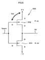
- such digital amplifier includes switching means 300 including a P-channel field effect transistor 302 and an N-channel field effect transistor 304.
- the source terminal of the P-channel field effect transistor 302 is connected to a first operation voltage +V, while the source terminal of the n-channel field effect transistor 304 is connected to a second operation voltage -V.
- the drain terminals of the P-channel field effect transistor 302 and the N-channel field effect transistor 304 are commonly connected to an output terminal.
- the gate terminals of the P-channel field effect transistor 302 and the N-channel field effect transistor 304 are commonly connected to an input terminal to which the above mentioned PMW type input signal Spwm is inputted.
- EP-A-1544996 which has a filing date of 25 July 2003 and a publication date of 22 June 2005 discloses a volume adjustment device having a digital amplifier with a gate drive circuit for driving output transistors.
- US5898340 discloses an audio amplifier with digital audio and volume inputs comprising a switching means with two transistors that are switched in response to an audio signal.
- US6388514 discloses a class D amplifier system having an adaptive power supply which adjusts the output voltage based on audio input levels to reduce switching losses at low audio input levels.
- the digital amplifier includes a switching means for outputting a driving signal by switching a DC voltage as the operation voltage in response to a pulse width modulation input signal and operation voltage control means for controlling the value of the operation voltage, wherein the switching means has input signal conversion means as well as first and second field effect transistors of mutually identical polarity, the drain of the first field effect transistor being connected to the operation voltage, the source of the first field effect transistor and the drain of the second field effect transistor being connected in common to the output terminal of the switching means, and the source of the second field effect transistor being connected to a designated reference voltage; and the input signal conversion means generates a first input signal in phase with the input signal and a second input signal of inverted phase with respect to the input signal with the first input signal being applied to the gate of the first field effect transistor and the
- the digital amplifier includes a switching means for outputting a driving signal by switching a DC voltage as the operation voltage in response to a pulse width modulation type input signal, and operation voltage controlling means for controlling the operation voltage
- the switching means has first and second input signal conversion means and first, second, third and fourth field effect transistors of identical polarity one another, the drains of the first and the third field effect transistors being connected to the operation voltage, the source of the first field effect transistor and the drain of the second field effect transistor being connected in common to a first output terminal of the switching means for outputting the driving signal, the source of the third field effect transistor and the drain of the fourth field effect transistor being connected in common to a second output terminal for outputting the driving signal, the sources of the second and fourth field effect transistors being connected to a designated reference voltage;
- the first input conversion means generates a first input signal in phase with the input signal and a second input signal of inverted phase with respect to the input signal, the first input signal being applied to the gate of the first field effect transistor
- the operation voltage is switched by the first and second field effect transistors of identical polarity with the drain of the first field effect transistor being connected to the operation voltage, the source of the first field effect transistor and the drain of the second field effect transistor being connected in common to the output terminal of the switching means for outputting the driving signal, the source of the second field effect transistor being supplied to the designated reference voltage, thereby enabling to set the gate-source voltages of the first and second field effect transistors regardless of the operation voltage and thus performing volume adjustment over a wide range without any restriction on the switching operation of the first and second field effect transistors by the operation voltage.
- the operation voltage is switched by the first, second, third and fourth field effect transistors of identical polarity.
- the drain of the first and third field effect transistors are connected to the operation voltage
- the source of the first field effect transistor and the drain of the second field effect transistor are connected in common to a first output terminal of the switching means for outputting the driving signal
- the source of the third field effect transistor and the drain of the fourth field effect transistor are connected in common to a second output terminal of the switching means for outputting the driving signal
- the sources of the second and fourth field effect transistors are connected to the reference potential, thereby enabling to set the gate-source voltages of the first, second, third and fourth field effect transistors without any restriction by the operation voltage.
- the operation voltage is switched by using a first and a second field effect transistors of identical polarity with each other.
- it is achieved by switching the operation voltage by using a first, second, third and fourth field effect transistors of identical polarity with one another.
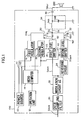
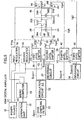
- FIG. 1 is a block diagram to show a simplified construction of an embodiment 1 of a digital amplifier according to a preferred embodiment of the present invention.
- a digital amplifier 100 is connected to an audio source such as, for example, a CD player, a DVD player or the like (not shown) for receiving a PCM type input signal Spcm from such audio source and supplies a driving signal Sdout to audio output means 200 such as a speaker or the like connected to the digital amplifier 100.
- an audio source such as, for example, a CD player, a DVD player or the like (not shown) for receiving a PCM type input signal Spcm from such audio source and supplies a driving signal Sdout to audio output means 200 such as a speaker or the like connected to the digital amplifier 100.
- the digital amplifier 100 includes a power supply unit 10, an operation unit 12, a micro computer 14, first and second regulators 16, 18, an over- sampling filter 20, a ⁇ modulation circuit 22, an inverter circuit 24, first and second level shifters 26, 28, first and second field effect transistors 30, 32, a low pass filter 34, a coupling capacitor 36 and the like. It is constructed so that the power supply unit 10 generates first and second voltages V1 and V2 which are constant DC voltages, wherein the first voltage V1 is supplied to the first regulator 16, while the second voltage V2 is supplied to the second regulator 18 and the second level shifter 28.
- the operation unit 12 includes an operation switch or an operation knob for volume adjustment under control by the user.
- volume setting data indicating the setting of the volume is inputted to the micro computer 14.
- the first regulator 16 generates the operation voltage Vreg which is a positive DC voltage to be supplied to the drain of the first field effect transistor 30 based on the first voltage V1 and the microcomputer 14 is constructed to control the operation voltage Vreg.
- the control of the operation voltage Vreg by the micro computer 14 is made in response to the above mentioned volume setting data which is generated by the operation of the operation unit 12.
- the second regulator 18 generates a third voltage V3 based on the second voltage V2 and the third voltage V3 is a DC voltage to be supplied to the first level shifter 26 based on the second voltage V2 under control of the micro computer 14.
- the control of the third voltage V3 by the micro computer will be described hereinafter.
- the over-sampling filter 20 receives the PCM type input signal Spcm and the ⁇ modulation circuit 22 receives the output signal from the over-sampling filter 20 to generate the PWM type input signal Spwm.
- the over-sampling filter 20 and the ⁇ modulation circuit 22 constitute an embodiment of pulse width modulation conversion means as recited in the claim.
- the input signal Spwm has a constant crest value with respect to the reference voltage (the ground potential in this example of preferred embodiment of the present invention) and the duty factor of the input signal Spwm is proportional to the amplitude of the driving signal Sd, i.e., volume.
- the inverter circuit 24 generates an input signal Srpwm which inverted the phase of the PWM type input signal Spwm outputted from the ⁇ modulation circuit 22.
- the input signal which is applied to the first level shifter 26 from the ⁇ modulation circuit 22 is referred to as a first input signal Spwm
- the input signal which is applied to the second level shifter 28 from the inverter circuit 24 is referred to as a second input signal Srpwm.
- the first level shifter 26 and the second level shifter 28 convert the amplitude (crest value) of the first and second input signal Spwm and Srpwm before being applied to the gates of the first and second field effect transistors 30 and 32, respectively.
- the first and second input signals Spwm and Srpwm outputted from the ⁇ modulation circuit 22 and the inverter circuit 24 have about 2V amplitude and are less than the minimum value of the gate-source voltage Vgs which is required for driving the first and second field effect transistors 30, 32, the first and second level shifters 26, 28 convert the amplitudes to about 6V. It is to be noted that the minimum value of the gate-source voltage Vgs differs depending on types and characteristics of such field effect transistor.
- the first level shifter 26 converts the amplitude of the first input signal Spwm based on the third voltage V3 which is supplied form the second regulator 18, the third voltage V3 increases or decreases under control of the micro computer 14, thereby increasing or decreasing the first input signal Spwm outputted from the first level shifter 26.
- the second level shifter 28 converts the amplitude of the second input signal Srpwm based on the constant second voltage V2 which is supplied from the power supply unit 10, the amplitude of the second input signal Srpwm outputted from the second level shifter 28 is constant.
- the first and second field effect transistors 30, 32 are the identical polarity with each other, i.e., the first and the second field effect transistors 30, 32 are N-channel field effect transistors in this example of preferred embodiment of the present invention.
- the first field effect transistor 30 has the drain connected to the operation voltage Vreg and the source connected to the drain of the second field effect transistor 32 and the gate for receiving the first input signal Spwm which is applied from the first level shifter 26, thereby performing on/off operation in response to the first input signal Spwm.
- the second field effect transistor 32 has the source connected to the ground potential as the reference voltage and the gate for receiving the second input signal Srpwm from the second level shifter 28 for performing on/off operation.
- the junction point of the source of the first field effect transistor 30 and the drain of the second field effect transistor 32 constitutes an output terminal 33 from which the PWM type driving signal Sd is outputted. Accordingly, since the first input signal Spwm inputted to the gate of the first field effect transistor 30 and the second input signal Srpwm inputted to the gate of the second field effect transistor 32 are inverted in phase with each other, the first field effect transistor 30 and the second field effect transistor 32 are driven in such a manner that one of them is in the on state while the other is in the off state. Therefore, in the condition when the first field effect transistor 30 is on and the second field effect transistor 32 is off, the operation voltage Vreg is outputted on the output point 33.
- the driving signal Sd is a PWM type signal having the same amplitude (crest value) as the operation voltage Vreg.
- the low pass filter 34 passes only signal components of the audio frequency bandwidth in the driving signal Sd which is applied from the output terminal 33, i.e., is constructed to convert the driving signal Sd into an audio signal of the audio bandwidth.
- the low pass filter 34 is an LC filter comprising an inductance 34A and a capacitor 34B.
- the coupling capacitor 36 eliminates DC component from the driving signal Sd which is applied from the low pass filter 34 and applies only AC components to the audio output means 200 as the driving signal Sdout.
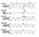
- FIG. 2 shows waveforms on various parts of the first and second field effect transistors 30, 32.
- FIG. 2 (A) is the gate voltage Vg1 of the first field effect transistor 30 (the first input signal Spwm applied from the first level shifter 26)
- FIG. 2 (B) is the driving signal Sd on the output terminal 33 (the source voltage of the first field effect transistor 30)
- FIG. 2 (C) is the gate-source voltage Vgs1 of the first field effect transistor 30
- FIG. 2 (D) is the gate voltage Vg2 of the second field effect transistor 32 (the second input signal Srpwm applied from the second level shifter 28)
- FIG. 2 (A) is the gate voltage Vg1 of the first field effect transistor 30 (the first input signal Spwm applied from the first level shifter 26)
- FIG. 2 (B) is the driving signal Sd on the output terminal 33 (the source voltage of the first field effect transistor 30)
- FIG. 2 (C) is the gate-source voltage Vgs1 of the first field effect transistor 30
- the gate-source voltage Vgs2 of the second field effect transistor 32 is the gate-source voltage Vgs2 of the second field effect transistor 32.
- the minimum gate-source voltages Vgs1 and Vgs2 required for operating the first and second field effect transistors 30, 32 are 5V.
- the operation voltage Vreg is 1V for a certain time interval t1.
- the operation voltage Vreg is 0.5V for a time interval t2.
- the gate voltage Vg1 is continued to remain as 6V as shown in the solid line (A)
- the on resistance between the drain and the source fluctuates, thereby resulting in degrading the distortion factor of the audio which is outputted from the audio output means 200.
- the present invention is constructed in such a manner that the micro computer 14 controls the amplitude of the gate voltage (first input signal) Vg1 in response to the change in the operation voltage Vreg to make the gate-source voltage Vgs1 of the first field effect transistor 30 substantially constant.
- the micro computer 14 controls the first level shifter 26 by way of the second regulator 18 and changes the amplitude of the gate voltage Vg1 from 6V (solid line) to 5.5V (dotted line) in response to the change of the operation voltage from 1V to 0.5V as shown in FIG. 2 (A) in the time interval t2, thereby maintaining the amplitude of the gate-source voltage Vgs1 at 5V (dotted line).
- the amplitude of the gate-source voltage Vgs2 of the second field effect transistor 32 remains the same amplitude as the gate voltage (the second input signal) Vg2 even if the operation voltage Vreg may change as shown in FIG. 2 (D) and (E) , thereby not exhibiting the phenomenon to change the on resistance between the drain-source of the second field effect transistor 32. Accordingly, unlike the case of the first field effect transistor 30, the second field effect transistor 32 has no need to control the amplitude of the gate voltage Vg2 in response to the operation voltage Vreg. This is the reason why the second voltage V2 which is supplied to the second level shifter 28 from the power supply 10 is fixed.
- the micro computer 14 and the first regulator 16 constitute an embodiment of the operation voltage control means as recited in the claims.
- the second regulator 18, the inverter circuit 24, the first level shifter 26 and second level shifter 28 constitute an embodiment of the input signal conversion means as recited in the claims.
- the micro computer 14, the second regulator 18 and the first level shifter 26 constitute an embodiment of the input signal control means as recited in the claims.
- the input signal conversion means and the first and second field effect transistors 30, 32 constitute an embodiment of the switching means as recited in the claims.
- the operation voltage control means, the input signal conversion means and the input signal control means are not restricted to the particular constructions in this example of preferred embodiment of the present invention. It is needless to say that they can be realized in various known circuit configurations.
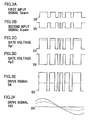
- the operation of the digital amplifier 100 having the above construction will be described as follows. Shown in FIG. 3 are waveforms on various parts of the digital amplifier. Assuming that the user operates the operation portion 12 to set the volume to, for example, a first value, the first regulator 16 is controlled by the micro computer 14 to set the operation voltage Vref to a value corresponding to the first value. As a result, the PCM type input signal Spcm is converted into the input signal Spwm by the over-sampling filter 20 and the ⁇ modulation circuit 22.
- the first input signal Spwm in phase with the input signal Spwm is applied to the first level shifter 26, while the second input signal Srpwm which is in a reverse phase relationship with the first input signal Spwm is applied to the second level shifter 28 ( FIG. 3 (A) and (B) .
- the gate voltage Vg1 is applied to the gate of the first field effect transistor 30 from the first level shifter 26, while the gate voltage Vg2 is applied to the gate of the second field effect transistor 32 from the second level shifter 28 ( FIG. 3 (C) and (D) ), thereby forcing the first and second field effect transistors 30, 32 to perform switching operation.
- the driving voltage Vreg is switched and the driving signal Sd is outputted from the output terminal 33 ( FIG.
- the driving signal Sd is converted into the audio signal of the audio bandwidth by the low pass filter 34 and applied to audio output menas 200 as the driving signal Sdout after eliminating the DC component by the coupling capacitor 36, thereby outputting the audio (sound) signal from the audio output means 200 ( FIG. 3 (F) , solid line).
- the first regulator 16 is controlled by the micro computer 14 so that the operation voltage Vreg is set to a value corresponding to the second value.
- the amplitude of the gate voltage Vg1 is controlled by the micro computer 14 in response to the change in the operation voltage Vreg so that the gate-source voltage Vgs1 of the first field effect transistor 30 remains substantially constant.
- the amplitude of the first input signal Vg1 is controlled to the value a shown by the solid line in FIG. 3 (C) in response to the change in the operation voltage Vreg, thereby maintaining the amplitude of the gate-source voltage Vgs1 substantially constant.
- the operation voltage Vreg as decreased in response to the second value is switched and the driving signal Sd of the reduced amplitude is outputted from the output terminal 33 as shown by the dotted line in FIG. 3 (E) .
- the amplitude of the driving signal Sd applied from the audio output means 200 is reduced as shown by the dotted line in FIG. 3 (F) , thereby reducing the volume of the audio (sound) signal outputted from the audio output means 200.
- the digital amplifier 100 exhibits the following advantages: 1) Because of the construction to switch the operation voltage Vreg by the first and second field effect transistors 30, 32 of identical polarity, connect the drain of the first field effect transistor 30 to the operation voltage Vreg, commonly connect the source of the first field effect transistor 30 and the drain of the second field effect transistor 32 to the output terminal 33 of the switching means for outputting the driving signal Sd and connect the source of the second field effect transistor 32 to the designated reference voltage, the gate-source voltages of the first and second field effect transistors 30, 32 can be set without being limited by the operation voltage Vreg, thereby eliminating the restriction by the switching operation by the operation voltage Vreg and providing volume adjustment over a wide range.
- FIG. 4 is a descriptive illustration to show noise spectrum and waveforms of the digital amplifier 100.
- FIG. 4 (A1) and (A2) are noise spectrum of the PCM type input signal Spcm in FIG. 1
- (B1) and (B2) are noise spectrum of the input signal Spwm after PWM conversion in FIG. 1
- (C1) and (C2) are waveforms of the driving signal Sd outputted from the output terminal 33
- (D1) and (D2) are noise spectrum of the driving signal Sdout to be applied to the audio output means 200.
- (A1), (B1), (C1) and (D1) correspond to the conditions when the volume is set to a large value
- (A2), (B2), (C2) and (D2) correspond to the conditions when the volume is set to a second value which is smaller than the first value
- the input signal Spcm contains both audio (solid line) and noise (dotted line). Although the noise level is less than the audio level, noise extends to a higher frequency bandwidth than the audio bandwidth. As shown in FIG. 4 (B1), among the noise component in the input signal Spwm in which PWM conversion is carried out on the input signal Spcm, the portion overlapping with the audio bandwidth is shifted to a higher frequency bandwidth than the audio bandwidth. However, such sifted noise component is a cause of audio quality degradation in the audio output. As shown in FIG. 4 (C1), since the volume is set to a relatively large first value, the driving signal Sd has a relatively large amplitude. As shown in FIG.
- the driving signal Sdout which passed through the low pass filter 34 and the coupling capacitor 36 contains the noise component which is similar to the case in FIG. 4 (B1).
- the volume is set to the second value which is relatively lower than the first value, the changes as shown in FIG. 4 (A2) through (D2) occur.
- the amplitude in the driving signal Sd is reduced as shown in FIG. 4 (C2) and the audio level as well as the noise level in the driving signal Sdout decrease as shown in FIG. 4 (D2).
- a conventional digital amplifier which is constructed to input the input signal Spcm to a digital amplifier and performing a PWM conversion on its output has an inherent problem in that the amplitude of the PWM type driving signal remains unchanged and not decreasing the noise level contained in the driving signal even if the volume is set to a low value, thereby degrading audio quality in a low volume setting.
- the amplitude of the gate voltage Vg1 is controlled by the input signal control means in response to the change in the operation voltage Vreg so that the gate-source voltage Vgs1 of the first field effect transistor 30 remains substantially constant in this example of preferred embodiment of the present invention.
- the input signal control means may be eliminated if the change in the on resistance due to the change in the gate-source voltage Vgsl is negligible.
- N-channel type is used for the first and second field effect transistors 30, 32 in this example of preferred embodiment of the present invention, similar advantages can be achieved by using P-channel type for the first and second field effect transistors 30, 32.
- the low pass filter 34 should not be restricted to the particular construction as shown in this example of preferred embodiment of the present invention and various other known constructions may be used for the low pass filter.
- the construction of the above mentioned PWM conversion means should not be restricted to the one comprising the over-sampling filter 20 and the ⁇ modulation circuit 22.
- volume adjustment means comprising a digital attenuator and the like for performing volume adjustment by bit shifting the digital data of the PCM type input signal Spcm at the front stage of the pulse width modulation conversion means, for example, at the front stage of the over-sampling filter 20.
- volume adjustment means it is advantageous for surely adjusting the amplitude of the driving signal Sd to zero or near zero by setting the digital data to zero or near zero.
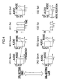
- FIG. 5 is a block diagram to show a simplified construction of the digital amplifier of the embodiment 2.
- the digital amplifier 100A includes an inverter circuit 38, third and fourth level shifters 40, 42, third and fourth field effect transistors 44, 46, a low pass filter 48 and the like in addition to the construction in the embodiment 1 but excludes the coupling capacitor 36 in the embodiment 1.
- the first regulator generates the operation voltage Vreg, a positive DC voltage to be supplied to drains of the first and third field effect transistors 30, 44 based on the first voltage V1 which is supplied from the power supply unit 10 and is constructed so that the operation voltage Vreg is controlled by the micro computer 14.
- the control of the operation voltage Vreg by the micro computer 14 is performed by the above mentioned volume setting data which is generated by the operation of the operation unit 12.
- the second regulator 18 generates the third voltage V3, a DC voltage to be supplied to the first and third level shifters 26, 42 based on the second voltage V2 and the third voltage V3 is controlled by the micro computer 14.
- the control of the third voltage V3 by the micro computer 14 will be described hereinafter.
- the inverter circuit 38 is constructed, in a similar way to the inverter circuit 24, to generate the input signal Srpwm having the inverted phase with respect to input signal Spwm from the ⁇ modulation circuit 22.
- the input signal to be applied to the first level shifter 26 from the ⁇ modulation circuit 22 is referred to as a first input signal Spwm1
- the input signal to be applied to the second level shifter 28 from the inverter circuit 24 is second input signal Srpwm2
- the input signal to be applied to the third level shifter 40 from the inverter circuit 38 is a third input signal Srpw3
- the input signal to be applied to the fourth level shifter 42 from the ⁇ modulation circuit 22 is a fourth input signal Spwm4.
- the third level shifter 40 and the fourth level shifter 42 perform respectively amplitude (crest value) conversion of the third and fourth input signals Srpwm3 and Spwm4 before being applied to the gates of the third and fourth field effect transistors 44 and 46 and such conversion is to secure the gate-source voltages Vgs which are required for driving the third and fourth field effect transistors 44 and 46, similar to the conversion by the first and second level shifters 26, 28.
- the third level shifter 40 converts the amplitude of the third input signal Srpwm 3 based on the third voltage V3 which is supplied from the second regulator 18, the third voltage V3 increases or decreases under control of the micro computer 14, thereby increasing or decreasing the amplitude of the third input signal Srpwm3 which is outputted from the third level shifter 40.
- the fourth level shifter 42 performs amplitude conversion of the fourth input signal Spwm4 based on the constant second voltage V2 which is supplied from the power supply unit 10, the fourth input signal Srpwm which is outputted from the fourth level shifter 28 remains constant.
- the first and second field effect transistors 30, 32 and the third and fourth field effect transistors 44, 46 include all field effect transistors of identical polarity and are the first through fourth field effect transistors 30, 32, 44, 46 are N-channel field effect transistors in this example of preferred embodiment of the present invention.
- the third field effect transistor 44 has the drain connected to the operation voltage Vreg, the source connected to the drain of the of the fourth field effect transistor 46 and the gate for receiving the third input signal Srpwm from the third level shifter 40 for on/off operation.
- the fourth field effect transistor 46 has the source connected to the ground potential as the reference voltage and the gate for receiving the fourth input signal Spwm from the fourth level shifter 42 for on/off operation.
- the junction point of the source of the third field effect transistor 44 and the drain of the fourth field effect transistor 46 constitutes the output terminal 47 from which the PWM type driving signal Sd2 is outputted.
- the output terminal 33 is referred to as a first output terminal 33
- the output terminal 47 is referred to as a second output terminal 47
- the driving signal outputted from the first output terminal 33 is referred to as a first driving signal Sd1
- the driving signal outputted from the second output terminal 47 is referred to as a second driving signal Sd2.
- the first and second driving signals Sd1 and Sd2 are PWM type signals having the same amplitude (crest value) equal to the operation voltage Vreg and opposite in phase with each other.
- the low pass filter 48 has the same construction as the low pass filter 34 and is constructed to convert the second driving signal Sd2 outputted from the second output terminal 47 into the audio signal in the audio bandwidth. Accordingly, the low pass filters 34, 48 are constructed to generate driving signals Sdout1 and Sdout2 which are audio signals having the opposite phases with each other. In this example of preferred embodiment of the present invention, the driving signals Sdout1 and Sdout2 are inputted to both input terminals of the audio output means 200 for driving the same.
- the switching means includes a full bridge circuit including four field effect transistors 30, 32, 44, 46.
- the micro computer 14 and the first regulator 16 constitute an embodiment of the operation voltage control means as recited in the claims.
- the second regulator 18, the inverter circuit 24, the first level shifter 26 and the second level shifter 28 constitute an embodiment of the first input signal conversion means as recited in the claims.
- the second regulator 18, the inverter circuit 38, the third level shifter 40 and the fourth level shifter 42 constitute an embodiment of the second input signal conversion means as recited in the claims.
- the micro computer 14, the second regulator 18, the first level shifter 26 and the third level shifter 40 constitute an embodiment of the input signal control means as recited in the claims.
- the first and second input signal conversion means and the first through fourth field effect transistors 30, 32, 44 and 44 constitute an embodiment of the switching means as recited in the claims.
- the operation voltage control means, the first and second input signal conversion means and the input signal control means should not be restricted to the constructions in this example of preferred embodiment of the present invention. Of course, they can be realized by using various known circuits. It is also possible to construct the second input signal Srpw2 outputted from the inverter circuit 24 to be applied to the third level shifter 40 as the third input signal Srpw3. In this case, the inverter circuit 38 is no longer needed, thereby advantageously simplifying the circuit and reducing cost and power consumption.
- This example of preferred embodiment of the present invention is constructed to control the amplitude of the gate voltages (first and third input signals) Vg1 and Vg3 in response to the change in the operation voltage Vreg so that the gate-source voltages of the first field effect transistor 30 and third field effect transistor 44 remain substantially constant. Since the amplitude control of the gate voltages Vg1 and Vg3 is substantially the same as the control operation of the gate voltage Vg1 as described in the embodiment 1, the detailed control operation is omitted and description will be made on signal waveforms on various parts when the gate voltages Vg1 and Vg2 are controlled and not controlled.
- FIG. 6 shows waveforms in the embodiment 2 when the gate voltages Vg1 and Vg3 are not controlled
- FIG. 7 shows waveforms in embodiment 1 when the gate voltages Vg1 and Vg3 are controlled.
- A shows the operation voltage Vreg
- B shows the first input signal Spwm1
- C shows the gate voltage Vg1 of the first field effect transistor 30
- D shows the gate voltage Vg2 of the second field effect transistor Vg2
- E) shows the first driving signal Sd1
- F shows the gate-source voltage Vgs1 of the first field effect transistor 30
- G shows the gate voltage Vg3 of the third field effect transistor 44
- H shows the gate voltage Vg4 of the fourth field effect transistor 46
- I shows the second driving signal Sd2
- J shows the gate-source voltage Vgs3 of the third field effect transistor 44.
- the gate voltages Vg1 and Vg3 are not controlled.
- the operation voltage Vreg is decreased, for example, from 2V to 1V by the operation of the volume adjustment
- the amplitudes of the first and the second driving signals Sd1 and Sd2 also decrease from 2V to 1V.
- the first-source voltages Vgs1 and Vgs2 of the first and third field effect transistors 344 may change, for example, from 3V to 4V as shown in FIG. 6 (F) and (J) . Therefore, the on resistances between the drain-source of the first and the third field effect transistors 30, 44 may fluctuate, thereby resulting in degrading the distortion factor of the audio which is outputted from the audio output means 200.
- the gate voltage Vg1 and Vg3 are controlled.
- the operation voltage Vreg is decreased, for example, from 2V to 1V by operating the volume adjustment
- the amplitudes of the first and second driving signals Sd1, Sd2 also decrease from 2V to 1V.
- the micro computer 14 controls the first and third level shifters 26, 40 by way of the second regulator 18, thereby controlling the amplitudes of the gate voltages Vg1 and Vg2 from 5V to 4V as shown in FIG.
- the first and second input signal control means can be eliminated if the change in the on resistances of the first and third field effect transistors 30, 44 is negligible.
- N-channel type transistors are used as the first through fourth field effect transistors 30, 32, 44 and 46 in this example of preferred embodiment of the present invention, the same advantages can be achieved by using P-channel transistors.
- the gate voltages Vg1, Vg2, Vg3, Vg4 are need to be negative voltages.
- Various known constructions may be used as the low pass filters 34, 48.
Landscapes
- Engineering & Computer Science (AREA)
- Power Engineering (AREA)
- Signal Processing (AREA)
- Amplifiers (AREA)
- Control Of Amplification And Gain Control (AREA)
Claims (7)
- Digitaler Verstärker (100) umfassend:eine Schalteinrichtung zur Abgabe eines Steuersignals (Sd) durch Schalten einer Betriebsspannung (Vreg), die durch eine Gleichspannung gebildet ist, auf der Grundlage eines Pulsbreitenmodulations-Eingangssignals (Spwm);eine Betriebsspannungs-Steuereinrichtung (12, 14, 16) zum Steuern des Wertes der Betriebsspannung (Vreg);wobei die Schalteinrichtung eine Eingangssignal-Umsetzeinrichtung (20, 22, 24, 26, 28) und einen ersten und einen zweiten Feldeffekttransistor (30, 32) von gemeinsamer identischer Polarität aufweist;wobei die Drain des ersten Feldeffekttransistors (30) mit der Betriebsspannung (Vreg) verbunden ist;wobei die Source des ersten Feldeffekttransistors (30) und die Drain des zweiten Feldeffekttransistors (32) gemeinsam an einem Ausgangsanschluss (33) der Schalteinrichtung angeschlossen sind;wobei die Source des zweiten Feldeffekttransistors (32) mit einer Referenzspannung verbunden ist;wobei die Eingangssignal-Umsetzeinrichtung (20, 22, 24, 26, 28) ein erstes Eingangssignal in Phase mit dem Eingangssignal und ein zweites Eingangssignal von bzw. mit einer invertierten Phase in Bezug auf das Eingangssignal erzeugt;und umfassend eine Eingangssignal-Steuereinrichtung (26) zum Steuern einer Amplitude des ersten Eingangssignals in Abhängigkeit von einer Spannung (V3), die durch die Betriebsspannungs-Steuereinrichtung (12, 14, 16, 18) auf die Betriebsspannung (Vreg) hin gesteuert ist, um eine Gate-Source-Spannung des ersten Feldeffekttransistors annähernd konstant zu machen;wobei das erste Eingangssignal dem Gate des ersten Feldeffekttransistors zugeführt wird, während das zweite Eingangssignal dem Gate des zweiten Feldeffekttransistors zugeführt wird;und ferner umfassend:eine Pulsbreitenmodulations-Umsetzeinrichtung (20, 22) zum Umsetzen eines pulscodierten Modulations- bzw. Pulscodemodulations-Eingangssignals in ein Pulsbreitenmodulations-Eingangssignal;wobei die Pulsbreitenmodulations-Umsetzeinrichtung ein Überabtastungs-Filter (20) zur Aufnahme des pulscodierten Modulations- bzw. Pulscodemodulations-Eingangssignals und eine Δ∑-Modulationsschaltung (22) zum Erzeugen des Pulsbreitenmodulations-Eingangssignals aus einem Ausgangssignal des Überabtastungs-Filters enthält.
- Digitaler Verstärker nach Anspruch 1, wobei die ersten und zweiten Feldeffekttransistoren (30, 32) vom N-Kanal-Typ sind und wobei die Betriebsspannung eine positive Spannung umfasst.
- Digitaler Verstärker nach Anspruch 1, wobei die ersten und zweiten Feldeffekttransistoren (30, 32) vom P-Kanal-Typ sind und wobei die Betriebsspannung eine negative Spannung umfasst.
- Digitaler Verstärker nach einem der Ansprüche 1 bis 3, ferner umfassend eine Pulsbreitenmodulations-Umsetzeinrichtung zum Umsetzen eines pulscodierten Modulations- bzw. Pulscodemodulations-Eingangssignals in ein Pulsbreitenmodulations-Eingangssignal,
wobei eine vordere Stufe der Pulsbreitenmodulations-Umsetzeinrichtung eine Lautstärke-Einstelleinrichtung aufweist, die zur Vornahme einer Lautstärkeeinstellung durch Bit-Verschiebung von Digitaldaten vorgesehen ist, welche das pulscodierte Modulations- bzw. Pulscodemodulations-Eingangssignal bilden. - Digitaler Verstärker nach Anspruch 1, wobei die Schalteinrichtung ferner umfasst:einen dritten und einen vierten Feldeffekttransistor von gemeinsamer identischer Polarität mit den ersten und zweiten Feldeffekttransistoren;wobei die Drain-Elektroden des ersten und des dritten Feldeffekttransistors mit der Betriebsspannung verbunden sind;wobei die Source-Elektroden des zweiten und des vierten Feldeffekttransistors mit einer Referenzspannung verbunden sind;wobei eine zweite Eingangssignal-Umsetzeinrichtung ein drittes Eingangssignal von invertierter Phase in Bezug auf das Eingangssignal und ein viertes Eingangssignal in Phase mit dem Eingangssignal erzeugt;und wobei das dritte Eingangssignal dem Gate des dritten Feldeffekttransistors zugeführt wird, während das vierte Eingangssignal dem Gate des vierten Feldeffekttransistors zugeführt wird;und wobei die Eingangssignal-Steuereinrichtung ferner betreibbar ist, um eine Amplitude des dritten Eingangssignals entsprechend einer Änderung in der Betriebsspannung zu steuern, um die Gate-Source-Spannung des dritten Feldeffekttransistors annähernd konstant zu machen.
- Digitaler Verstärker nach Anspruch 5, wobei die ersten, zweiten, dritten und vierten Feldeffekttransistoren vom N-Kanal-Typ sind und wobei die Betriebsspannung eine positive Spannung umfasst.
- Digitaler Verstärker nach Anspruch 5, wobei die ersten, zweiten, dritten und vierten Feldeffekttransistoren vom P-Kanal-Typ sind und wobei die Betriebsspannung eine negative Spannung umfasst.
Applications Claiming Priority (2)
| Application Number | Priority Date | Filing Date | Title |
|---|---|---|---|
| JP2003327741A JP3928728B2 (ja) | 2003-09-19 | 2003-09-19 | デジタルアンプ |
| JP2003327741 | 2003-09-19 |
Publications (2)
| Publication Number | Publication Date |
|---|---|
| EP1517438A1 EP1517438A1 (de) | 2005-03-23 |
| EP1517438B1 true EP1517438B1 (de) | 2011-07-20 |
Family
ID=34191376
Family Applications (1)
| Application Number | Title | Priority Date | Filing Date |
|---|---|---|---|
| EP04255592A Expired - Lifetime EP1517438B1 (de) | 2003-09-19 | 2004-09-15 | Digitaler Verstärker |
Country Status (4)
| Country | Link |
|---|---|
| US (1) | US7170339B2 (de) |
| EP (1) | EP1517438B1 (de) |
| JP (1) | JP3928728B2 (de) |
| KR (1) | KR101053011B1 (de) |
Cited By (1)
| Publication number | Priority date | Publication date | Assignee | Title |
|---|---|---|---|---|
| US8995691B2 (en) | 2008-07-14 | 2015-03-31 | Audera Acoustics Inc. | Audio amplifier |
Families Citing this family (13)
| Publication number | Priority date | Publication date | Assignee | Title |
|---|---|---|---|---|
| JP4967257B2 (ja) * | 2005-06-03 | 2012-07-04 | パナソニック株式会社 | デジタルアンプ方法及びデジタルアンプ回路 |
| US7495509B2 (en) * | 2006-12-06 | 2009-02-24 | Panasonic Corporation Co., Ltd. | Audio power amplifier |
| JP2009033335A (ja) * | 2007-07-25 | 2009-02-12 | Sony Corp | 増幅回路および増幅回路の制御方法、増幅装置、ならびに、再生装置 |
| JP5231151B2 (ja) * | 2008-10-01 | 2013-07-10 | ルネサスエレクトロニクス株式会社 | デジタルアンプシステム |
| JP2011060394A (ja) * | 2009-09-11 | 2011-03-24 | Elpida Memory Inc | 半導体装置及びデータ処理システム |
| US8295510B2 (en) * | 2010-03-16 | 2012-10-23 | Sound Cheers Limited | Power-saving amplifying device |
| KR101067489B1 (ko) * | 2010-04-13 | 2011-09-27 | 송병일 | Opt에 class-d 샘플링주파수를 공급하여 경량화된 전관방송증폭기 |
| CN103873984A (zh) * | 2012-12-13 | 2014-06-18 | 鸿富锦精密工业(武汉)有限公司 | 自动调节电子装置输出音量的系统及方法 |
| WO2015136413A1 (en) * | 2014-03-12 | 2015-09-17 | Semiconductor Energy Laboratory Co., Ltd. | Semiconductor device |
| US9559642B2 (en) | 2015-01-02 | 2017-01-31 | Logitech Europe, S.A. | Audio delivery system having an improved efficiency and extended operation time between recharges or battery replacements |
| EP3402070B1 (de) * | 2017-05-11 | 2020-02-12 | Infineon Technologies Austria AG | Klasse-d-audio-verstärker mit einstellbarer gateansteuerung |
| CN110649898B (zh) * | 2019-10-21 | 2023-04-07 | 严添明 | 一种自动双向限幅宽带d类音频功率放大器的前置放大器 |
| JP2023124998A (ja) * | 2022-02-28 | 2023-09-07 | 株式会社Cri・ミドルウェア | 音声出力回路 |
Citations (1)
| Publication number | Priority date | Publication date | Assignee | Title |
|---|---|---|---|---|
| EP1544996A1 (de) * | 2002-07-29 | 2005-06-22 | Sharp Kabushiki Kaisha | VOLUMENEINSTELLEINRICHTUNG, DIGITALER VERSTûRKER UND DIGITALSIGNAL-WIEDERGABEEINRICHTUNG |
Family Cites Families (9)
| Publication number | Priority date | Publication date | Assignee | Title |
|---|---|---|---|---|
| US4992749A (en) * | 1988-12-28 | 1991-02-12 | Pioneer Electronic Corporation | Pulse-width modulating amplifier circuit |
| US5767740A (en) * | 1996-09-27 | 1998-06-16 | Harris Corporation | Switching amplifier closed loop dual comparator modulation technique |
| US5898340A (en) * | 1996-11-20 | 1999-04-27 | Chatterjee; Manjirnath A. | High power efficiency audio amplifier with digital audio and volume inputs |
| JP2000223965A (ja) * | 1998-11-04 | 2000-08-11 | Rohm Co Ltd | オ―ディオ増幅回路およびこの回路を用いたオ―ディオ装置 |
| US6388514B1 (en) * | 1998-12-23 | 2002-05-14 | International Rectifier Corporation | Class D high voltage amplifier system with adaptive power supply |
| GB9911505D0 (en) * | 1999-05-19 | 1999-07-14 | New Transducers Ltd | Transducer driver |
| JP2001202696A (ja) | 2000-01-17 | 2001-07-27 | Alpine Electronics Inc | デジタルアンプ |
| SE0104403D0 (sv) * | 2001-12-21 | 2001-12-21 | Bang & Olufsen Powerhouse As | Attenuation control for digital power converters |
| US6925115B1 (en) * | 2002-12-23 | 2005-08-02 | Cirrus Logic, Inc. | Apparatus and method for safely handling asychronous shutdown of pulsewidth modulated output |
-
2003
- 2003-09-19 JP JP2003327741A patent/JP3928728B2/ja not_active Expired - Fee Related
-
2004
- 2004-09-15 EP EP04255592A patent/EP1517438B1/de not_active Expired - Lifetime
- 2004-09-17 US US10/944,585 patent/US7170339B2/en not_active Expired - Lifetime
- 2004-09-17 KR KR1020040074451A patent/KR101053011B1/ko not_active Expired - Fee Related
Patent Citations (1)
| Publication number | Priority date | Publication date | Assignee | Title |
|---|---|---|---|---|
| EP1544996A1 (de) * | 2002-07-29 | 2005-06-22 | Sharp Kabushiki Kaisha | VOLUMENEINSTELLEINRICHTUNG, DIGITALER VERSTûRKER UND DIGITALSIGNAL-WIEDERGABEEINRICHTUNG |
Cited By (1)
| Publication number | Priority date | Publication date | Assignee | Title |
|---|---|---|---|---|
| US8995691B2 (en) | 2008-07-14 | 2015-03-31 | Audera Acoustics Inc. | Audio amplifier |
Also Published As
| Publication number | Publication date |
|---|---|
| JP3928728B2 (ja) | 2007-06-13 |
| KR101053011B1 (ko) | 2011-07-29 |
| JP2005094589A (ja) | 2005-04-07 |
| US20050062527A1 (en) | 2005-03-24 |
| US7170339B2 (en) | 2007-01-30 |
| EP1517438A1 (de) | 2005-03-23 |
| KR20050028825A (ko) | 2005-03-23 |
Similar Documents
| Publication | Publication Date | Title |
|---|---|---|
| EP1517438B1 (de) | Digitaler Verstärker | |
| KR101118867B1 (ko) | 전력 증폭 회로, dc-dc 컨버터, 피크 홀딩 회로, 및 피크 홀딩 회로를 포함하는 출력 전압 제어 회로 | |
| US7659754B2 (en) | CMOS power switching circuit usable in DC-DC converter | |
| US8643436B2 (en) | Multi-level boosted Class D amplifier | |
| US5378932A (en) | Level shifting circuit | |
| US5594386A (en) | Pulse width modulated amplifier | |
| US6388477B1 (en) | Switchable voltage follower and bridge driver using the same | |
| US7382160B2 (en) | Differential output circuit with reduced differential output variation | |
| US10034085B2 (en) | Class-D amplifier, audio processing apparatus and method of driving class-D amplifier | |
| US6448851B1 (en) | Amplifier with offset compensation for a high voltage output transistor stage | |
| US6781458B2 (en) | Providing DC isolation in switching amplifiers | |
| US7230481B2 (en) | System and method for reducing audible artifacts in an audio system | |
| US7227413B1 (en) | Audio amplification device with antipop circuitry | |
| US6084467A (en) | Analog amplifier clipping circuit | |
| US6278322B1 (en) | Transconductance amplifier and automatic gain control device using it | |
| EP1825592B1 (de) | Leistungsvervielfachervorrichtung und -verfahren | |
| US7449948B2 (en) | Amplifier | |
| US20090115519A1 (en) | Power amplifier and its idling current setting circuit | |
| KR20040047779A (ko) | 스위치 모드 회로에서 출력 임피던스 정합을 위한 회로 및방법 | |
| US20220255516A1 (en) | Amplification circuit with compensation for common-mode voltage fluctuation | |
| US5945851A (en) | Current source apparatus with bias switches | |
| JP2005210329A (ja) | デジタルアンプ | |
| US20060132233A1 (en) | Integrated circuit devices having a control circuit for biasing an amplifier output stage and methods of operating the same | |
| JP7437227B2 (ja) | D級増幅器 | |
| JP2022051329A (ja) | D級アンプ |
Legal Events
| Date | Code | Title | Description |
|---|---|---|---|
| PUAI | Public reference made under article 153(3) epc to a published international application that has entered the european phase |
Free format text: ORIGINAL CODE: 0009012 |
|
| AK | Designated contracting states |
Kind code of ref document: A1 Designated state(s): AT BE BG CH CY CZ DE DK EE ES FI FR GB GR HU IE IT LI LU MC NL PL PT RO SE SI SK TR |
|
| AX | Request for extension of the european patent |
Extension state: AL HR LT LV MK |
|
| 17P | Request for examination filed |
Effective date: 20050907 |
|
| AKX | Designation fees paid |
Designated state(s): DE GB NL |
|
| 17Q | First examination report despatched |
Effective date: 20080228 |
|
| GRAP | Despatch of communication of intention to grant a patent |
Free format text: ORIGINAL CODE: EPIDOSNIGR1 |
|
| GRAS | Grant fee paid |
Free format text: ORIGINAL CODE: EPIDOSNIGR3 |
|
| GRAA | (expected) grant |
Free format text: ORIGINAL CODE: 0009210 |
|
| AK | Designated contracting states |
Kind code of ref document: B1 Designated state(s): DE GB NL |
|
| REG | Reference to a national code |
Ref country code: GB Ref legal event code: FG4D |
|
| REG | Reference to a national code |
Ref country code: DE Ref legal event code: R096 Ref document number: 602004033523 Country of ref document: DE Effective date: 20110908 |
|
| REG | Reference to a national code |
Ref country code: NL Ref legal event code: T3 |
|
| PLBE | No opposition filed within time limit |
Free format text: ORIGINAL CODE: 0009261 |
|
| STAA | Information on the status of an ep patent application or granted ep patent |
Free format text: STATUS: NO OPPOSITION FILED WITHIN TIME LIMIT |
|
| 26N | No opposition filed |
Effective date: 20120423 |
|
| REG | Reference to a national code |
Ref country code: DE Ref legal event code: R097 Ref document number: 602004033523 Country of ref document: DE Effective date: 20120423 |
|
| REG | Reference to a national code |
Ref country code: DE Ref legal event code: R084 Ref document number: 602004033523 Country of ref document: DE |
|
| REG | Reference to a national code |
Ref country code: DE Ref legal event code: R084 Ref document number: 602004033523 Country of ref document: DE Effective date: 20150410 |
|
| PGFP | Annual fee paid to national office [announced via postgrant information from national office to epo] |
Ref country code: NL Payment date: 20190918 Year of fee payment: 16 |
|
| PGFP | Annual fee paid to national office [announced via postgrant information from national office to epo] |
Ref country code: GB Payment date: 20190920 Year of fee payment: 16 |
|
| PGFP | Annual fee paid to national office [announced via postgrant information from national office to epo] |
Ref country code: DE Payment date: 20200925 Year of fee payment: 17 |
|
| REG | Reference to a national code |
Ref country code: NL Ref legal event code: MM Effective date: 20201001 |
|
| GBPC | Gb: european patent ceased through non-payment of renewal fee |
Effective date: 20200915 |
|
| PG25 | Lapsed in a contracting state [announced via postgrant information from national office to epo] |
Ref country code: NL Free format text: LAPSE BECAUSE OF NON-PAYMENT OF DUE FEES Effective date: 20201001 |
|
| PG25 | Lapsed in a contracting state [announced via postgrant information from national office to epo] |
Ref country code: GB Free format text: LAPSE BECAUSE OF NON-PAYMENT OF DUE FEES Effective date: 20200915 |
|
| REG | Reference to a national code |
Ref country code: DE Ref legal event code: R119 Ref document number: 602004033523 Country of ref document: DE |
|
| PG25 | Lapsed in a contracting state [announced via postgrant information from national office to epo] |
Ref country code: DE Free format text: LAPSE BECAUSE OF NON-PAYMENT OF DUE FEES Effective date: 20220401 |