US5767740A - Switching amplifier closed loop dual comparator modulation technique - Google Patents
Switching amplifier closed loop dual comparator modulation technique Download PDFInfo
- Publication number
- US5767740A US5767740A US08/722,354 US72235496A US5767740A US 5767740 A US5767740 A US 5767740A US 72235496 A US72235496 A US 72235496A US 5767740 A US5767740 A US 5767740A
- Authority
- US
- United States
- Prior art keywords
- bridge
- output
- amplifier
- complementary
- signal
- Prior art date
- Legal status (The legal status is an assumption and is not a legal conclusion. Google has not performed a legal analysis and makes no representation as to the accuracy of the status listed.)
- Expired - Fee Related
Links
- 230000009977 dual effect Effects 0.000 title claims abstract description 23
- 238000000034 method Methods 0.000 title description 4
- 230000000295 complement effect Effects 0.000 claims description 19
- 230000005236 sound signal Effects 0.000 claims 1
- 239000003990 capacitor Substances 0.000 description 3
- 238000001914 filtration Methods 0.000 description 3
- 238000012935 Averaging Methods 0.000 description 1
- 230000002411 adverse Effects 0.000 description 1
- 230000007812 deficiency Effects 0.000 description 1
- 230000000694 effects Effects 0.000 description 1
- 230000008030 elimination Effects 0.000 description 1
- 238000003379 elimination reaction Methods 0.000 description 1
Images


Classifications
-
- H—ELECTRICITY
- H03—ELECTRONIC CIRCUITRY
- H03F—AMPLIFIERS
- H03F3/00—Amplifiers with only discharge tubes or only semiconductor devices as amplifying elements
- H03F3/20—Power amplifiers, e.g. Class B amplifiers, Class C amplifiers
- H03F3/21—Power amplifiers, e.g. Class B amplifiers, Class C amplifiers with semiconductor devices only
- H03F3/217—Class D power amplifiers; Switching amplifiers
- H03F3/2173—Class D power amplifiers; Switching amplifiers of the bridge type
-
- H—ELECTRICITY
- H03—ELECTRONIC CIRCUITRY
- H03K—PULSE TECHNIQUE
- H03K7/00—Modulating pulses with a continuously-variable modulating signal
- H03K7/08—Duration or width modulation ; Duty cycle modulation
-
- H—ELECTRICITY
- H03—ELECTRONIC CIRCUITRY
- H03F—AMPLIFIERS
- H03F2200/00—Indexing scheme relating to amplifiers
- H03F2200/03—Indexing scheme relating to amplifiers the amplifier being designed for audio applications
Definitions
- This invention relates in general to switching Class D audio amplifiers and, in particular, to full bridge dual comparator audio Class D amplifiers.
- FIG. 1A A classical single comparator pwm amplifier is shown in FIG. 1A.
- the audio input is fed into an integrating amplifier 11.
- the output of the integrator 11 is fed into a single comparator 12.
- the other input to comparator 12 is a modulating triangle wave.
- the output of comparator 12 is a pulse width modulated signal representing the desired output.
- the pwm output is used to drive one pair of mosfets on one side of the H-bridge 20.
- a complementary pwm signal is generated by inverting the pwm output of comparator 12.
- the complementary pwm signal is used to drive the other pair of mosfets on the other side of the full bridge 24.
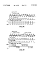
- FIG. 2A shows the wave forms associated with the single comparator pwm architecture. All four gate drive signals to the H-bridge are derived from the single pwm signal output from the comparator 12 of FIG. 1A. That architecture has only two output states defined for the load across terminals 20 and 22, +VBUS and -VBUS respectively. When there is no audio input, the output at the speaker must be zero. To achieve an output of zero at the speaker, the H-bridge must produce a square wave with a 50% duty cycle switching between +VBUS and -VBUS. An output filter 70 averages the square wave to produce a zero output at the speaker. If the output filter 70 is removed from this circuit, the speaker itself must perform the averaging of the bridge output. Because of the resistive nature of the speaker, the RMS power at the switching frequency would be dissipated in the speaker. This is unacceptable and the dual comparator architecture of FIG. 2A overcomes that deficiency.
- FIG. 1B shows a typical prior art dual comparator pwm amplifier.
- Such a dual comparator pwm amplifier does not require a filter.
- There an audio input is fed into a first comparator 12.
- the audio input is also fed into an inverting amplifier 14 and from there into a second comparator 16.
- Each comparator also receives a modulating triangular wave signal.
- the respective comparators 12, 16 output a series of pulses V A , V B that drive the power mosfets in full bridge 50.
- Inverters 36, 38 connected to the outputs of pwm comparators 12, 16 generate complementary pulses. So, gate driver circuit 18 receives input pulses AHI, ALI, BHI and BLI.
- the gate driver circuit 18 may include DMOS or quasi-vertical DMOS power transistors that generate output gate driver signals AHO, BHO, ALO, and BLO. Those output signals are applied to the gates of the power mosfets 52, 54, 56, and 58 in the full H-bridge 24.
- Bridge output terminals 20, 22 are connected across a speaker 26.
- the output terminals 20, 22 are also coupled via amplifiers 30, 32 to the respective inputs A and B of the bridge driver circuit 18 and provide feedback signals for the signals AHI, ALI, BHI, and BLI.
- FIG. 2B shows a dual comparator switching technique performed by the circuit shown in FIG 1B.
- FIG. 2B requires two pulse trains V A , V B , representing the two pwm comparator outputs 12, 16, to define all four gate voltages for the H-bridge 24.
- the H-bridge output voltages across the speaker has three output states, +VBUS, -VBUS, and 0V.
- the addition of the 0V output state eliminates the need for a bridge output filter. This is especially true at light loads where the output of bridge 24 is zero for a large portion of the audio period when small +VBUS and -VBUS spikes are averaged to produce the peaks of the low amplitude sign wave output.
- the speaker 26 acts as its own filter to convert the pulses back to analog auto signals.
- the architecture of FIG. 1B cannot precisely match the output of the H-bridge to the audio input. This is due to the presence of two feedback paths, one for each control signal.
- the feedback paths are closed so that each side of the bridge 50 is forced to track the square wave of the output from one of the two pulse width modulators.
- One feedback path is from output 20 via inverter 30 to the AHI and ALI input of gate driver circuit 18 and the other is from output 22 via inverter 32 to the BHI and BLI inputs of gate driver circuit 18.
- the paths are closed so that the opposite sides of the bridge 24 are forced to track one of the square wave inputs V A and V B from the pulse width modulators 12, 16.
- One drawback of this technique is that the differential output voltage of the H-bridge 24 is not tracked and only a limited range of feedback is allowed.
- the bridge output voltage is in the order of 60-80 volts, whereas the gate driver circuit 18 is of the order of about 5 volts.
- the feedback from the H-bridge has to be reduced from 60-80 volts to about 5 volts and such reduction adversely affects the accuracy of the feedback.
- the dual feedback path design results in poor power supply rejection and increased harmonic distortion.
- the invention provides a dual comparator pulse width modulated switching audio Class D amplifier that has a novel feedback technique.
- a differential amplifier converts the output of the H-bridge into a single ended feedback signal.
- the feedback signal is summed with the audio input signal and integrated to produce a control voltage for one comparator.
- the control voltage for the other comparator is generated by inverting the control voltage of the first comparator.
- the second input to both comparators is a triangle wave.
- the outputs of the two comparators, the pwm signals, are applied to a gate driver circuit and the gate driver circuit drives the gates of four mosfets configured as an H-bridge.
- the load or speaker is connected directly across the outputs of the H-bridge without the need for any filtering.
- the feedback path and the input integrator smooth and scale the output pulses of the H bridge and the circuit more accurately tracks the input signal.
- FIG. 1A shows a prior art single comparator pwm amplifier
- FIG. 1B shows a prior art dual comparator pwm amplifier
- FIG. 2A shows operating wave forms for the single pwm amplifier of FIG. 1;
- FIG. 2B shows operating wave forms for the for the dual pwm, dual feedback loop amplifier of FIG. 1b;
- FIG. 3 shows a closed loop dual comparator pwm amplifier with a differential signal ended and integrating feedback loop.
- FIG. 3 shows the dual comparator single feedback loop pwm amplifier of the invention.
- the H-bridge outputs at terminals 20, 22 are fed into a differential amplifier 40 which produces a single ended output signal.
- Each of the inputs to 40 pass through a low pass filter comprising a capacitor 60 and a resistor 62.
- the low pass filters limit the slew rate of the differential amplifier inputs to be less than the slew rate of the amplifier 40 to reduce distortion.
- the output of 40 is an inverted representation of the voltage across the speaker and is also opposite in sign to the audio input.
- the resistors RF1 and RF2 scale the voltage level of the output of the amplifier 40 to the voltage level of the audio input.
- the feedback signal from 40 is applied to the summing node 41.
- the audio input is also applied to he summing node 41.
- the voltage at the summing node 41 represents the difference between the audio input and the amplifier output and is commonly referred to as the error signal.
- the error signal is applied to the integrator 42 that has feedback capacitor 43.
- the output of the integrating amplifier 42 is the control signal CTL+ for one side of the H-bridge 24, i.e. for AHO and ALO.
- Signal CTL+ is coupled to an inverting amplifier 14 to generate a second control signal CTL- which controls the other side of the H bridge 24, i.e. BHO and BLO.
- the complimentary control signals CTL+ and CTL- are input to the pwm comparators 12 and 16 respectively.
- a modulating triangle wave reference signal is also input to both comparators 12, 16.
- Comparators 12, 16 and inverters 36, 38 generate the gate driver input signals including a first pair of complementary input low voltage gate driver signals, AHI, ALI, and a second pair of complementary gate driver signals, BHI, BLI.
- the gate driver circuit 18 generates the output high voltage drive signals, AHO, ALO,BHO, BLO required to drive the gates of the high current transistors (mosfets) of the H-bridge.
- the output gate driver signals are applied to the gates of the mosfets in the full bridge 24 and the speaker 26 is connected across the bridge between terminals 20 and 22.
- the drive signals at output terminals 20, 22 of the H-bridge are square wave pulses similar to the H-bridge output pulses shown in FIG. 2B and they drive the speaker 26.
- the outputs 20, 22 are also connected to the filters 60, 62 of the differential amplifier 40.
- the filtered output signals are input to amplifier 40.
- the single ended output of amplifier 40 is a feedback signal representing the output of the Class D amplifier.
- the feedback signal is summed with the audio input at a node 41 to provide the error signal.
- the integrator 42 receives the error signals and generates an output signal CTL+.
- An inverter 14 coupled to the output CTL+ generates a complementary control signal CTL-.
- the integrator 42 performs two functions. First, it integrates the error signal on node 41.
- integrator 42 in that way will adjust the gate driver control signals CTL+ and CTL- until the error signal is driven to zero and the output is exactly equal to the audio input. Second, it provides reconstruction filtering. Since the feedback signal output from 40 is still pulse-like, the integrator 42 will smooth the control signals CTL+ and CTL- which are used by the pwm comparators 12, 16. The modulating reference triangle wave signals are coupled to both comparators 12, 16. The inverters 36, 38 then generate the complementary gate driver signals AHI, ALI, BHI, BLI.
Abstract
Description
Claims (7)
Priority Applications (6)
| Application Number | Priority Date | Filing Date | Title |
|---|---|---|---|
| US08/722,354 US5767740A (en) | 1996-09-27 | 1996-09-27 | Switching amplifier closed loop dual comparator modulation technique |
| TW086113613A TW348341B (en) | 1996-09-27 | 1997-09-19 | Switching amplifier closed loop dual comparator modulation technique |
| EP97402203A EP0833443B1 (en) | 1996-09-27 | 1997-09-23 | Switching amplifier closed loop dual comparator modulation technique |
| DE69704188T DE69704188D1 (en) | 1996-09-27 | 1997-09-23 | Switch amplifier with two comparator modulation and negative feedback |
| KR1019970049098A KR19980025038A (en) | 1996-09-27 | 1997-09-26 | Switching audio amplifier |
| JP9263014A JPH10126170A (en) | 1996-09-27 | 1997-09-29 | Modulation method for switching amplifier closed loop dual comparator |
Applications Claiming Priority (1)
| Application Number | Priority Date | Filing Date | Title |
|---|---|---|---|
| US08/722,354 US5767740A (en) | 1996-09-27 | 1996-09-27 | Switching amplifier closed loop dual comparator modulation technique |
Publications (1)
| Publication Number | Publication Date |
|---|---|
| US5767740A true US5767740A (en) | 1998-06-16 |
Family
ID=24901509
Family Applications (1)
| Application Number | Title | Priority Date | Filing Date |
|---|---|---|---|
| US08/722,354 Expired - Fee Related US5767740A (en) | 1996-09-27 | 1996-09-27 | Switching amplifier closed loop dual comparator modulation technique |
Country Status (6)
| Country | Link |
|---|---|
| US (1) | US5767740A (en) |
| EP (1) | EP0833443B1 (en) |
| JP (1) | JPH10126170A (en) |
| KR (1) | KR19980025038A (en) |
| DE (1) | DE69704188D1 (en) |
| TW (1) | TW348341B (en) |
Cited By (34)
| Publication number | Priority date | Publication date | Assignee | Title |
|---|---|---|---|---|
| US5917369A (en) * | 1998-02-25 | 1999-06-29 | National Semiconductor Corporation | Pulse width modulator with automatic gain control over-voltage modulator and limiter |
| WO2000014870A1 (en) * | 1998-09-09 | 2000-03-16 | The Engineering Consortium, Inc. | Battery polarity insensitive integrated circuit amplifier |
| US6107875A (en) * | 1998-10-15 | 2000-08-22 | Intersil Corporation | Variable frequency class D modulator with built in soft clipping and frequency limiting |
| US6108182A (en) * | 1998-10-30 | 2000-08-22 | Intersil Corporation | Overcurrent sensing circuit and self adjusting blanking |
| WO2000059114A1 (en) * | 1999-03-29 | 2000-10-05 | Anacon Systems, Inc. | Method and apparatus for providing pulse width modulation |
| US6373336B1 (en) * | 1998-07-24 | 2002-04-16 | Texas Instruments, Copenhagen Aps | Method of attenuating zero crossing distortion and noise in an amplifier, an amplifier and uses of the method and the amplifier |
| US6441685B1 (en) * | 2000-03-17 | 2002-08-27 | Jl Audio, Inc. | Amplifier circuit and method for providing negative feedback thereto |
| US20030027455A1 (en) * | 2001-07-31 | 2003-02-06 | Yazaki Corporation | Electrical connector having terminal locking structure |
| US20030030486A1 (en) * | 2001-07-31 | 2003-02-13 | Yamaha Corporation | Pulse-width modulation circuit and power amplifier circuit |
| US20030090318A1 (en) * | 2001-01-18 | 2003-05-15 | Tae-Ha Ryoo | Digital power amplifier |
| US20030095000A1 (en) * | 2001-11-16 | 2003-05-22 | Acoustic Technology, Inc. | Apparatus with ultra high output power class D audio amplifier |
| US6724305B2 (en) * | 2001-05-25 | 2004-04-20 | Golden West Sales | Pulse induction silverware detector |
| US20040125968A1 (en) * | 1996-06-05 | 2004-07-01 | Intersil Americas Inc. | Monolithic class D amplifier |
| US20040232979A1 (en) * | 2003-05-23 | 2004-11-25 | Edwards Christopher Francis | Efficient minimum pulse spread spectrum modulation for filterless class d amplifiers |
| US20050029994A1 (en) * | 2003-08-08 | 2005-02-10 | Onkyo Corporation | Pulse-width modulation circuit and switching amplifier using the same |
| US20050062527A1 (en) * | 2003-09-19 | 2005-03-24 | Hiroshi Saito | Digital amplifier |
| US20050162222A1 (en) * | 2004-01-22 | 2005-07-28 | Rahmi Hezar | Amplifier using delta-sigma modulation |
| US20060077005A1 (en) * | 2003-02-04 | 2006-04-13 | Samsung Electronics Co., Ltd. | Current controlled pulse width modulation circuit and class-D amplifier comprising the same |
| US20070116109A1 (en) * | 2005-11-18 | 2007-05-24 | Harman International Industries, Incorporated | System for dynamic time offsetting in interleaved power amplifiers |
| US20080042743A1 (en) * | 2006-08-17 | 2008-02-21 | Matsushita Electric Industrial Co., Ltd. | Differential input class d amplifier |
| US20080118092A1 (en) * | 2006-11-20 | 2008-05-22 | Ming-Hsiung Chen | Speaker System of utilizing Pulse Width Modulation Signals for Saving Idling Power Consumption |
| US20080197935A1 (en) * | 2004-09-14 | 2008-08-21 | Nxp N.V. | Arrangement for Pulse-Width Modulating an Input Signal |
| US20100052792A1 (en) * | 2006-09-14 | 2010-03-04 | Koichi Nose | Amplifying apparatus, method of output control and control program |
| US7705672B1 (en) * | 2007-02-12 | 2010-04-27 | Manuel De Jesus Rodriguez | Buck converters as power amplifier |
| US20110221529A1 (en) * | 2005-09-28 | 2011-09-15 | Yamaha Corporation | Class d amplifier |
| CN101512897B (en) * | 2006-07-12 | 2012-01-25 | 哈曼国际工业有限公司 | Amplifier employing interleaved signals for PWM ripple suppression |
| US8212613B1 (en) | 2011-09-21 | 2012-07-03 | Wen-Hsiung Hsieh | Switching amplifier using flyback transformer |
| US8228118B1 (en) | 2011-09-17 | 2012-07-24 | Wen-Hsiung Hsieh | Switching amplifier using capacitor for transmitting energy |
| US8410851B1 (en) | 2011-09-12 | 2013-04-02 | Wen-Hsiung Hsieh | Switching amplifier with an inductor |
| US8451056B2 (en) | 2011-03-15 | 2013-05-28 | Dongbu Hitek Co., Ltd. | Apparatus for outputting symmetrical signal and amplifier circuit |
| US20130335143A1 (en) * | 2012-06-14 | 2013-12-19 | Princeton Technology Corporation | Class-d power amplifier capable of reducing electromagnetic interference and triangular wave generator thereof |
| US8829945B2 (en) | 2011-07-05 | 2014-09-09 | Silicon Laboratories Inc. | Circuit and method for dynamic biasing of an output stage |
| US20150188502A1 (en) * | 2014-01-02 | 2015-07-02 | Samsung Electronics Co., Ltd. | Switching amplifier, sound output device, and audio apparatus using the same |
| US20150365059A1 (en) * | 2013-02-26 | 2015-12-17 | Kyocera Corporation | Class-d amplifier and electronic apparatus |
Families Citing this family (14)
| Publication number | Priority date | Publication date | Assignee | Title |
|---|---|---|---|---|
| GB2343573A (en) * | 1998-11-04 | 2000-05-10 | Applic Solutions Ltd | An efficient PWM switched amplifier with variable carrier frequency |
| DE19929841C2 (en) * | 1999-06-29 | 2001-07-12 | Jan Quellmann | Clocked amplifier, in particular for amplifying audio signals |
| JP3813045B2 (en) * | 2000-02-29 | 2006-08-23 | ローム株式会社 | H-bridge driver |
| US6404251B1 (en) * | 2000-03-27 | 2002-06-11 | Linear Technology Corporation | Systems and methods for linearly varying a pulse-width modulation signal with a control signal |
| US6882219B2 (en) | 2000-03-31 | 2005-04-19 | Ling Dynamic Systems | High frequency switch-mode power amplifier |
| GB2360889B (en) * | 2000-03-31 | 2004-04-28 | Ling Dynamic Systems | High frequency switch-mode power amplifier |
| JP2002034286A (en) * | 2000-07-17 | 2002-01-31 | Nec Corp | H-bridge-type motor-driving circuit |
| EP1351380A1 (en) * | 2002-04-02 | 2003-10-08 | Dialog Semiconductor GmbH | Class D amplifier energy control |
| JP2005057519A (en) * | 2003-08-05 | 2005-03-03 | Onkyo Corp | Pulse-width modulation circuit and switching amplifier with same circuit |
| JP4566566B2 (en) * | 2004-01-21 | 2010-10-20 | パナソニック株式会社 | Power amplifier |
| JP5022840B2 (en) * | 2007-09-13 | 2012-09-12 | ローム株式会社 | Amplifying device and acoustic apparatus using the same |
| KR101272595B1 (en) * | 2011-12-12 | 2013-06-11 | 기아자동차주식회사 | Dc motor pwm control apparatus and method for the same |
| KR101390519B1 (en) * | 2012-06-20 | 2014-05-27 | 한양대학교 에리카산학협력단 | multi-phase inverter topology for motor drives |
| CN103883508A (en) * | 2014-04-19 | 2014-06-25 | 湖南科技学院 | Automatic electronic type air pump control device |
Citations (12)
| Publication number | Priority date | Publication date | Assignee | Title |
|---|---|---|---|---|
| US3579132A (en) * | 1969-11-14 | 1971-05-18 | Ltv Ling Altec Inc | Class {37 d{38 {0 linear audio amplifier |
| US4004246A (en) * | 1974-06-06 | 1977-01-18 | Osamu Hamada | Pulse width modulated signal amplifier |
| US4059807A (en) * | 1974-11-02 | 1977-11-22 | Sony Corporation | Pulse width modulated amplifier |
| US4249136A (en) * | 1978-05-23 | 1981-02-03 | Sony Corporation | PWM Signal power amplifier |
| US4403196A (en) * | 1981-04-22 | 1983-09-06 | The United States Of America As Represented By The Secretary Of The Air Force | Pulse width modulated power amplifier with differential connecting line voltage drop comparators |
| US4554512A (en) * | 1984-08-27 | 1985-11-19 | Aerotech, Inc. | Switching amplifier with MOSFET driver circuit |
| US4949048A (en) * | 1988-12-28 | 1990-08-14 | Pioneer Electronic Corporation | Pulse width modulation amplifier circuit |
| US5014016A (en) * | 1989-04-13 | 1991-05-07 | Beltone Electronics Corporation | Switching amplifier |
| US5115205A (en) * | 1990-12-28 | 1992-05-19 | Square D Company | AC amplifier with automatic DC compensation |
| US5160896A (en) * | 1992-02-18 | 1992-11-03 | Harman International Industries, Incorporated | Class D amplifier |
| US5410592A (en) * | 1993-06-04 | 1995-04-25 | Harris Corporation | Class `D` audio speaker amplifier circuit with state variable feedback control |
| US5479337A (en) * | 1993-11-30 | 1995-12-26 | Kaiser Aerospace And Electronics Corporation | Very low power loss amplifier for analog signals utilizing constant-frequency zero-voltage-switching multi-resonant converter |
Family Cites Families (4)
| Publication number | Priority date | Publication date | Assignee | Title |
|---|---|---|---|---|
| JPS57170606A (en) * | 1981-04-10 | 1982-10-20 | Sony Corp | Amplifying circuit for pulse-width-modulated signal |
| JP3132280B2 (en) * | 1994-02-17 | 2001-02-05 | 松下電器産業株式会社 | Class D power amplifier |
| DE19512383A1 (en) * | 1995-04-01 | 1996-10-10 | Nokia Deutschland Gmbh | Class=D audio power amplifier |
| US5672998A (en) * | 1995-08-09 | 1997-09-30 | Harris Corporation | Class D amplifier and method |
-
1996
- 1996-09-27 US US08/722,354 patent/US5767740A/en not_active Expired - Fee Related
-
1997
- 1997-09-19 TW TW086113613A patent/TW348341B/en active
- 1997-09-23 EP EP97402203A patent/EP0833443B1/en not_active Expired - Lifetime
- 1997-09-23 DE DE69704188T patent/DE69704188D1/en not_active Expired - Lifetime
- 1997-09-26 KR KR1019970049098A patent/KR19980025038A/en not_active Application Discontinuation
- 1997-09-29 JP JP9263014A patent/JPH10126170A/en active Pending
Patent Citations (12)
| Publication number | Priority date | Publication date | Assignee | Title |
|---|---|---|---|---|
| US3579132A (en) * | 1969-11-14 | 1971-05-18 | Ltv Ling Altec Inc | Class {37 d{38 {0 linear audio amplifier |
| US4004246A (en) * | 1974-06-06 | 1977-01-18 | Osamu Hamada | Pulse width modulated signal amplifier |
| US4059807A (en) * | 1974-11-02 | 1977-11-22 | Sony Corporation | Pulse width modulated amplifier |
| US4249136A (en) * | 1978-05-23 | 1981-02-03 | Sony Corporation | PWM Signal power amplifier |
| US4403196A (en) * | 1981-04-22 | 1983-09-06 | The United States Of America As Represented By The Secretary Of The Air Force | Pulse width modulated power amplifier with differential connecting line voltage drop comparators |
| US4554512A (en) * | 1984-08-27 | 1985-11-19 | Aerotech, Inc. | Switching amplifier with MOSFET driver circuit |
| US4949048A (en) * | 1988-12-28 | 1990-08-14 | Pioneer Electronic Corporation | Pulse width modulation amplifier circuit |
| US5014016A (en) * | 1989-04-13 | 1991-05-07 | Beltone Electronics Corporation | Switching amplifier |
| US5115205A (en) * | 1990-12-28 | 1992-05-19 | Square D Company | AC amplifier with automatic DC compensation |
| US5160896A (en) * | 1992-02-18 | 1992-11-03 | Harman International Industries, Incorporated | Class D amplifier |
| US5410592A (en) * | 1993-06-04 | 1995-04-25 | Harris Corporation | Class `D` audio speaker amplifier circuit with state variable feedback control |
| US5479337A (en) * | 1993-11-30 | 1995-12-26 | Kaiser Aerospace And Electronics Corporation | Very low power loss amplifier for analog signals utilizing constant-frequency zero-voltage-switching multi-resonant converter |
Cited By (55)
| Publication number | Priority date | Publication date | Assignee | Title |
|---|---|---|---|---|
| US20040125968A1 (en) * | 1996-06-05 | 2004-07-01 | Intersil Americas Inc. | Monolithic class D amplifier |
| US20060238241A1 (en) * | 1996-06-05 | 2006-10-26 | Intersil Americas Inc. | Monolithic class d amplifier |
| US7076070B2 (en) | 1996-06-05 | 2006-07-11 | Intersil Americas Inc. | Monolithic class D amplifier |
| US5917369A (en) * | 1998-02-25 | 1999-06-29 | National Semiconductor Corporation | Pulse width modulator with automatic gain control over-voltage modulator and limiter |
| US6373336B1 (en) * | 1998-07-24 | 2002-04-16 | Texas Instruments, Copenhagen Aps | Method of attenuating zero crossing distortion and noise in an amplifier, an amplifier and uses of the method and the amplifier |
| US6157252A (en) * | 1998-09-09 | 2000-12-05 | The Engineering Consortium, Inc. | Battery polarity insensitive integrated circuit amplifier |
| WO2000014870A1 (en) * | 1998-09-09 | 2000-03-16 | The Engineering Consortium, Inc. | Battery polarity insensitive integrated circuit amplifier |
| US6107875A (en) * | 1998-10-15 | 2000-08-22 | Intersil Corporation | Variable frequency class D modulator with built in soft clipping and frequency limiting |
| US6108182A (en) * | 1998-10-30 | 2000-08-22 | Intersil Corporation | Overcurrent sensing circuit and self adjusting blanking |
| WO2000059114A1 (en) * | 1999-03-29 | 2000-10-05 | Anacon Systems, Inc. | Method and apparatus for providing pulse width modulation |
| US6867645B1 (en) | 1999-03-29 | 2005-03-15 | Daydreams Llc | Method and apparatus for providing pulse width modulation |
| US6441685B1 (en) * | 2000-03-17 | 2002-08-27 | Jl Audio, Inc. | Amplifier circuit and method for providing negative feedback thereto |
| US20030090318A1 (en) * | 2001-01-18 | 2003-05-15 | Tae-Ha Ryoo | Digital power amplifier |
| US6737917B2 (en) * | 2001-01-18 | 2004-05-18 | Dlogix Co., Ltd. | Digital power amplifier |
| US6724305B2 (en) * | 2001-05-25 | 2004-04-20 | Golden West Sales | Pulse induction silverware detector |
| US6778011B2 (en) | 2001-07-31 | 2004-08-17 | Yamaha Corporation | Pulse-width modulation circuit and power amplifier circuit |
| US20030030486A1 (en) * | 2001-07-31 | 2003-02-13 | Yamaha Corporation | Pulse-width modulation circuit and power amplifier circuit |
| US20030027455A1 (en) * | 2001-07-31 | 2003-02-06 | Yazaki Corporation | Electrical connector having terminal locking structure |
| US20030095000A1 (en) * | 2001-11-16 | 2003-05-22 | Acoustic Technology, Inc. | Apparatus with ultra high output power class D audio amplifier |
| US7151404B2 (en) * | 2003-02-04 | 2006-12-19 | Samsung Electronics Co., Ltd. | Current controlled pulse width modulation circuit and class-D amplifier comprising the same |
| US20060077005A1 (en) * | 2003-02-04 | 2006-04-13 | Samsung Electronics Co., Ltd. | Current controlled pulse width modulation circuit and class-D amplifier comprising the same |
| US6847257B2 (en) * | 2003-05-23 | 2005-01-25 | Maxim Integrated Products, Inc. | Efficient minimum pulse spread spectrum modulation for filterless class D amplifiers |
| US20040232979A1 (en) * | 2003-05-23 | 2004-11-25 | Edwards Christopher Francis | Efficient minimum pulse spread spectrum modulation for filterless class d amplifiers |
| US20050029994A1 (en) * | 2003-08-08 | 2005-02-10 | Onkyo Corporation | Pulse-width modulation circuit and switching amplifier using the same |
| US7102405B2 (en) * | 2003-08-08 | 2006-09-05 | Onkyo Corporation | Pulse-width modulation circuit and switching amplifier using the same |
| US20050062527A1 (en) * | 2003-09-19 | 2005-03-24 | Hiroshi Saito | Digital amplifier |
| US7170339B2 (en) * | 2003-09-19 | 2007-01-30 | Sony Corporation | Digital amplifier |
| US6998910B2 (en) * | 2004-01-22 | 2006-02-14 | Texas Instruments Incorporated | Amplifier using delta-sigma modulation |
| US20050162222A1 (en) * | 2004-01-22 | 2005-07-28 | Rahmi Hezar | Amplifier using delta-sigma modulation |
| US20080197935A1 (en) * | 2004-09-14 | 2008-08-21 | Nxp N.V. | Arrangement for Pulse-Width Modulating an Input Signal |
| US7868711B2 (en) | 2004-09-14 | 2011-01-11 | Nxp B.V. | Arrangement for pulse-width modulating an input signal |
| US8299853B2 (en) | 2005-09-28 | 2012-10-30 | Yamaha Corporation | Class D amplifier |
| US8054129B2 (en) | 2005-09-28 | 2011-11-08 | Yamaha Corporation | Class D amplifier |
| US20110221529A1 (en) * | 2005-09-28 | 2011-09-15 | Yamaha Corporation | Class d amplifier |
| US7778324B2 (en) | 2005-11-18 | 2010-08-17 | Harman International Industries, Incorporated | System for dynamic time offsetting in interleaved power amplifiers |
| US20070116109A1 (en) * | 2005-11-18 | 2007-05-24 | Harman International Industries, Incorporated | System for dynamic time offsetting in interleaved power amplifiers |
| CN101512897B (en) * | 2006-07-12 | 2012-01-25 | 哈曼国际工业有限公司 | Amplifier employing interleaved signals for PWM ripple suppression |
| US20080042743A1 (en) * | 2006-08-17 | 2008-02-21 | Matsushita Electric Industrial Co., Ltd. | Differential input class d amplifier |
| US7446603B2 (en) | 2006-08-17 | 2008-11-04 | Matsushita Electric Industrial Co., Ltd. | Differential input Class D amplifier |
| US8115540B2 (en) * | 2006-09-14 | 2012-02-14 | Nec Corporation | Amplifying apparatus, method of output control and control program |
| US20100052792A1 (en) * | 2006-09-14 | 2010-03-04 | Koichi Nose | Amplifying apparatus, method of output control and control program |
| US20080118092A1 (en) * | 2006-11-20 | 2008-05-22 | Ming-Hsiung Chen | Speaker System of utilizing Pulse Width Modulation Signals for Saving Idling Power Consumption |
| US7844061B2 (en) * | 2006-11-20 | 2010-11-30 | Princeton Technology Corporation | Speaker system of utilizing pulse width modulation signals for saving idling power consumption |
| US7705672B1 (en) * | 2007-02-12 | 2010-04-27 | Manuel De Jesus Rodriguez | Buck converters as power amplifier |
| US8451056B2 (en) | 2011-03-15 | 2013-05-28 | Dongbu Hitek Co., Ltd. | Apparatus for outputting symmetrical signal and amplifier circuit |
| US8829945B2 (en) | 2011-07-05 | 2014-09-09 | Silicon Laboratories Inc. | Circuit and method for dynamic biasing of an output stage |
| US8410851B1 (en) | 2011-09-12 | 2013-04-02 | Wen-Hsiung Hsieh | Switching amplifier with an inductor |
| US8228118B1 (en) | 2011-09-17 | 2012-07-24 | Wen-Hsiung Hsieh | Switching amplifier using capacitor for transmitting energy |
| US8212613B1 (en) | 2011-09-21 | 2012-07-03 | Wen-Hsiung Hsieh | Switching amplifier using flyback transformer |
| US20130335143A1 (en) * | 2012-06-14 | 2013-12-19 | Princeton Technology Corporation | Class-d power amplifier capable of reducing electromagnetic interference and triangular wave generator thereof |
| US8872581B2 (en) * | 2012-06-14 | 2014-10-28 | Princeton Technology Corporation | Class-D power amplifier capable of reducing electromagnetic interference and triangular wave generator thereof |
| US20150365059A1 (en) * | 2013-02-26 | 2015-12-17 | Kyocera Corporation | Class-d amplifier and electronic apparatus |
| US9667208B2 (en) * | 2013-02-26 | 2017-05-30 | Kyocera Corporation | Class-D amplifier and electronic apparatus |
| US20150188502A1 (en) * | 2014-01-02 | 2015-07-02 | Samsung Electronics Co., Ltd. | Switching amplifier, sound output device, and audio apparatus using the same |
| US9899972B2 (en) * | 2014-01-02 | 2018-02-20 | Samsung Electronics Co., Ltd. | Switching amplifier, sound output device, and audio apparatus using the same |
Also Published As
| Publication number | Publication date |
|---|---|
| KR19980025038A (en) | 1998-07-06 |
| TW348341B (en) | 1998-12-21 |
| DE69704188D1 (en) | 2001-04-12 |
| JPH10126170A (en) | 1998-05-15 |
| EP0833443B1 (en) | 2001-03-07 |
| EP0833443A1 (en) | 1998-04-01 |
Similar Documents
| Publication | Publication Date | Title |
|---|---|---|
| US5767740A (en) | Switching amplifier closed loop dual comparator modulation technique | |
| US6175272B1 (en) | Pulse—width modulation system | |
| US7456685B2 (en) | Class D audio amplifier with PWM and feedback | |
| EP1579570B1 (en) | Delta-sigma amplifiers with output stage supply voltage variation compensation and methods and digital amplifier systems using the same | |
| JP3982342B2 (en) | Triangular wave generation circuit in class D amplifier and class D amplifier using the triangular wave generation circuit | |
| US7142050B2 (en) | Recovery from clipping events in a class D amplifier | |
| US6952131B2 (en) | Digital PWM input D class amplifier by PWM negative feedback | |
| US6707337B2 (en) | Self-operating PWM amplifier | |
| KR100775184B1 (en) | Class-d amplifier | |
| US8013677B2 (en) | One-sided switching pulse width modulation amplifiers | |
| US5663647A (en) | Switching gradient amplifier with adjustable DC bus voltage | |
| JPH02177607A (en) | Pulse width modulating amplification circuit | |
| JP2003115730A (en) | Pwm (pulse-width modulation) circuit and power amplifier circuit | |
| JPS6252963B2 (en) | ||
| EP1825592B1 (en) | A power multiplier apparatus and method | |
| US10749486B2 (en) | Class D amplifier current feedback | |
| US7183818B2 (en) | Triangular wave generating circuit adapted to class-D amplifier | |
| US7279966B2 (en) | Systems for pseudo-BD modulation | |
| US20050127991A1 (en) | Volume control in class D amplifier using variable supply voltage | |
| US6538504B1 (en) | Switching amplifier crossover distortion reduction technique | |
| EP1184973A1 (en) | Power amplification equipment | |
| JPH0681054B2 (en) | Digital-to-analog converter with linearity control function | |
| JP4017596B2 (en) | Switching amplifier | |
| EP3926829A1 (en) | Modulator circuit, corresponding device and method | |
| US11159132B2 (en) | Class D amplifier stereo to mono converter |
Legal Events
| Date | Code | Title | Description |
|---|---|---|---|
| AS | Assignment |
Owner name: HARRIS CORPORATION, FLORIDA Free format text: ASSIGNMENT OF ASSIGNORS INTEREST;ASSIGNOR:FOGG, JOHN K.;REEL/FRAME:008256/0595 Effective date: 19960918 |
|
| AS | Assignment |
Owner name: HARRIS CORPORATION, FLORIDA Free format text: (ASSIGNMENT OF ASSIGNOR'S INTEREST) RE-RECORD TO CORRECT THE RECORDATION DATE OF 9-18-96 TO 9-27-96, PREVIOUSLY RECORDED AT REEL 8256, FRAME 0595.;ASSIGNOR:FOGG, JOHN K.;REEL/FRAME:008311/0635 Effective date: 19960918 |
|
| AS | Assignment |
Owner name: INTERSIL CORPORATION, FLORIDA Free format text: ASSIGNMENT OF ASSIGNORS INTEREST;ASSIGNOR:HARRIS CORPORATION;REEL/FRAME:010247/0043 Effective date: 19990813 |
|
| AS | Assignment |
Owner name: CREDIT SUISSE FIRST BOSTON, AS COLLATERAL AGENT, N Free format text: SECURITY INTEREST;ASSIGNOR:INTERSIL CORPORATION;REEL/FRAME:010351/0410 Effective date: 19990813 |
|
| AS | Assignment |
Owner name: RED CHIP COMPANY LTD., (A BRITISH VIRGIN ISLANDS C Free format text: ASSIGNMENT OF ASSIGNORS INTEREST;ASSIGNOR:INTERSIL CORPORATION, (A DELAWARE CORPORATION);REEL/FRAME:011044/0101 Effective date: 20000720 |
|
| AS | Assignment |
Owner name: RED CHIP COMPANY LTD., VIRGIN ISLANDS, BRITISH Free format text: ASSIGNMENT OF ASSIGNORS INTEREST;ASSIGNOR:INTERSIL CORPORATION;REEL/FRAME:011284/0578 Effective date: 20000720 |
|
| REMI | Maintenance fee reminder mailed | ||
| LAPS | Lapse for failure to pay maintenance fees | ||
| STCH | Information on status: patent discontinuation |
Free format text: PATENT EXPIRED DUE TO NONPAYMENT OF MAINTENANCE FEES UNDER 37 CFR 1.362 |
|
| FP | Lapsed due to failure to pay maintenance fee |
Effective date: 20020616 |
|
| AS | Assignment |
Owner name: RED CHIP COMPANY LTD (A BRITISH VIRGIN ISLANDS COR Free format text: CORRECTIVE ASSIGNMENT TO CORRECT THE TO REMOVE INCORRECT SERIAL NOS. 09/073,111 AND09/183,379 AND 09/437,939 PREVIOUSLY RECORDED ON REEL 011044 FRAME 0101. ASSIGNOR(S) HEREBY CONFIRMS THE ASSIGNMENT;ASSIGNOR:INTERSIL CORPORATION (A DELAWARE CORPORATION);REEL/FRAME:033118/0658 Effective date: 20000720 |