EP1513070B1 - Système avec un memoire attachable et détachable et une méthode correspondante - Google Patents
Système avec un memoire attachable et détachable et une méthode correspondante Download PDFInfo
- Publication number
- EP1513070B1 EP1513070B1 EP04255333A EP04255333A EP1513070B1 EP 1513070 B1 EP1513070 B1 EP 1513070B1 EP 04255333 A EP04255333 A EP 04255333A EP 04255333 A EP04255333 A EP 04255333A EP 1513070 B1 EP1513070 B1 EP 1513070B1
- Authority
- EP
- European Patent Office
- Prior art keywords
- voltage
- subsystem
- supply voltage
- host
- responsive
- Prior art date
- Legal status (The legal status is an assumption and is not a legal conclusion. Google has not performed a legal analysis and makes no representation as to the accuracy of the status listed.)
- Expired - Lifetime
Links
Images



Classifications
-
- G—PHYSICS
- G11—INFORMATION STORAGE
- G11C—STATIC STORES
- G11C16/00—Erasable programmable read-only memories
- G11C16/02—Erasable programmable read-only memories electrically programmable
- G11C16/06—Auxiliary circuits, e.g. for writing into memory
- G11C16/30—Power supply circuits
-
- G—PHYSICS
- G06—COMPUTING OR CALCULATING; COUNTING
- G06F—ELECTRIC DIGITAL DATA PROCESSING
- G06F13/00—Interconnection of, or transfer of information or other signals between, memories, input/output devices or central processing units
- G06F13/14—Handling requests for interconnection or transfer
- G06F13/16—Handling requests for interconnection or transfer for access to memory bus
- G06F13/1668—Details of memory controller
- G06F13/1694—Configuration of memory controller to different memory types
Definitions
- the flash memory may include a control circuit to generate a control signal responsive to the predetermined command and an internal supply-voltage generation circuit to convert an external supply voltage into an internal supply voltage where the internal supply-voltage generation circuit outputs the internal supply voltage having the same voltage level as the external supply voltage responsive to the control signal.
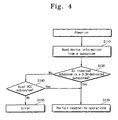
- the host 120 determines whether the NAND flash memory 144 operates at either 3.3V or 1.8V (S240). If the subsystem 140 operates at either 3.3V or 1.8V, the host 120 outputs a predetermined voltage set command according to predetermined timing (S250). The voltage set command is transmitted to the NAND flash memory 144 through a controller 142, and the control circuit 270 of the NAND flash memory enables the control signal nDUAL_VCC_EN responsive to the voltage set command. When the control signal nDUAL_VCC_EN is enabled, the NMOS transistor 313 is turned on.
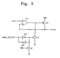
- the PMOS transistor 312 has the gate connected to the ground voltage through the NMOS transistor 313 regardless of the comparator 311, and the PMOS transistor 312 is fully turned on. Accordingly, the external supply voltage EVC is transmitted to the internal supply voltage IVC without the voltage drop of the PMOS transistor 312. That is, the internal supply voltage IVC is identical with the external supply voltage EVC.
Landscapes
- Engineering & Computer Science (AREA)
- Theoretical Computer Science (AREA)
- Physics & Mathematics (AREA)
- General Engineering & Computer Science (AREA)
- General Physics & Mathematics (AREA)
- Read Only Memory (AREA)
- Techniques For Improving Reliability Of Storages (AREA)
- Power Sources (AREA)
Claims (13)
- Procédé destiné à commander un sous-système (140) et un hôte (120), dans lequel ledit hôte (120) présente une tension de fonctionnement, le procédé comprenant les étapes consistant à :lire des informations de dispositif partir d'une mémoire (144) du sous-système (140) ;déterminer si le sous-système (140) fonctionne à une pluralité de tensions en réponse aux informations de dispositif, etfournit une commande prédéterminée au sous-système (140) de manière à remplacer la tension de fonctionnement du sous-système (140) par la tension de fonctionnement de l'hôte (120) en réponse à la détermination.
- Procédé de commande selon la revendication 1, comprenant l'étape consistant à exploiter le sous-système (140) à des première ou seconde tensions, la seconde tension étant inférieure à la première tension.
- Procédé de commande selon la revendication 2, comprenant l'étape consistant à exploiter le sous-système (140) à la première tension en réponse à la fourniture.
- Procédé de commande selon la revendication 2, comprenant l'étape consistant à exploiter le sous-système (140) à la seconde tension en réponse à la fourniture.
- Procédé de commande selon la revendication 2, dans lequel l'étape de lecture inclut l'étape consistant à lire à partir d'une mémoire flash NON-ET (NAND) (144).
- Procédé de commande selon la revendication 2, comprenant les étapes consistant à :générer un signal de commande en réponse à la commande prédéterminée ; etconvertir une tension d'alimentation externe en une tension d'alimentation interne ;où la tension d'alimentation interne présente environ le même niveau que la tension d'alimentation externe sensible au signal de commande.
- Système comprenant :un hôte (120) agencé pour fonctionner à une tension de fonctionnement; etun sous-système (140) couplé de manière opérationnelle à l'hôte (120) et ayant une mémoire (144);dans lequel l'hôte (120) est agencé pour lire des informations de dispositif à partir de la mémoire (144), afin de déterminer si le sous-système (140) fonctionne à une pluralité de tensions ; et
dans lequel l'hôte (120) est agencé pour fournir une commande prédéterminée au sous-système (140) laquelle remplace la tension de fonctionnement du sous-système (140) par la tension de fonctionnement de l'hôte (120) en réponse aux informations de dispositif. - Système selon la revendication 7, dans lequel le sous-système (140) est agencé pour être exploité à des première ou seconde tensions, la seconde tension étant inférieure à la première tension.
- Système selon la revendication 8, dans lequel le sons-système (140) est agencé pour être exploité à la première tension en réponse à la commande prédéterminée.
- Système selon la revendication 8, dans lequel le sous-système (140) est agencé pour être exploité à la seconde tension en réponse à la commande prédéterminée.
- Système selon la revendication 8, dans lequel le sous-système (140) inclut une mémoire flash NON-ET (144).
- Système selon la revendication 8, dans lequel le sous-système (140) comporte :un circuit de commande (270) destiné à générer un signal de commande en réponse à la commande prédéterminée; etun circuit de génération de tension d'alimentation interne (310) pour convertir une tension d'alimentation externe en une tension d'alimentation interne ;dans lequel le circuit de génération de tension d'alimentation interne est agencé pour générer en sortie la tension d'alimentation externe comme la tension d'alimentation interne sensible au signal de commande.
- Système selon la revendication 12, dans lequel le circuit de génération de tension d'alimentation interne (310) comporte :un transistor PMOS (312) connecté entre la tension d'alimentation externe et la tension d'alimentation interne ;un comparateur (311) pour commander le transistor PMOS (312) en réponse à la tension d'alimentation interne ; etun transistor NMOS (313) connecté entre une grille du transistor PMOS (312) et une tension de masse, et commandé par le signal de commande.
Applications Claiming Priority (2)
| Application Number | Priority Date | Filing Date | Title |
|---|---|---|---|
| KR1020030061089A KR100560767B1 (ko) | 2003-09-02 | 2003-09-02 | 탈착 가능한 저장 장치를 포함하는 시스템 및 그것의 제어방법 |
| KR2003061089 | 2003-09-02 |
Publications (3)
| Publication Number | Publication Date |
|---|---|
| EP1513070A2 EP1513070A2 (fr) | 2005-03-09 |
| EP1513070A3 EP1513070A3 (fr) | 2005-04-13 |
| EP1513070B1 true EP1513070B1 (fr) | 2008-12-31 |
Family
ID=34132222
Family Applications (1)
| Application Number | Title | Priority Date | Filing Date |
|---|---|---|---|
| EP04255333A Expired - Lifetime EP1513070B1 (fr) | 2003-09-02 | 2004-09-02 | Système avec un memoire attachable et détachable et une méthode correspondante |
Country Status (5)
| Country | Link |
|---|---|
| US (1) | US7617335B2 (fr) |
| EP (1) | EP1513070B1 (fr) |
| JP (1) | JP4707352B2 (fr) |
| KR (1) | KR100560767B1 (fr) |
| DE (1) | DE602004018719D1 (fr) |
Families Citing this family (22)
| Publication number | Priority date | Publication date | Assignee | Title |
|---|---|---|---|---|
| US7864615B2 (en) * | 2005-02-25 | 2011-01-04 | Kingston Technology Corporation | Flash memory controller utilizing multiple voltages and a method of use |
| US20090077393A1 (en) * | 2005-04-27 | 2009-03-19 | Matsushita Electric Industrial Co., Ltd. | Card-type electronic device and host device |
| US7631245B2 (en) * | 2005-09-26 | 2009-12-08 | Sandisk Il Ltd. | NAND flash memory controller exporting a NAND interface |
| US8291295B2 (en) * | 2005-09-26 | 2012-10-16 | Sandisk Il Ltd. | NAND flash memory controller exporting a NAND interface |
| US7436708B2 (en) * | 2006-03-01 | 2008-10-14 | Micron Technology, Inc. | NAND memory device column charging |
| KR100761470B1 (ko) * | 2006-07-31 | 2007-09-27 | 삼성전자주식회사 | 프로그램 디스터브를 방지할 수 있는 플래시 메모리 장치및 그것의 프로그램 방법 |
| US20080046641A1 (en) * | 2006-08-21 | 2008-02-21 | Sandisk Il Ltd. | NAND flash memory controller exporting a logical sector-based interface |
| US20080046630A1 (en) * | 2006-08-21 | 2008-02-21 | Sandisk Il Ltd. | NAND flash memory controller exporting a logical sector-based interface |
| CN101910972B (zh) * | 2008-02-29 | 2013-03-20 | 松下电器产业株式会社 | 主装置用接口装置、附属装置用接口装置、主装置、附属装置、通信系统、以及接口电压切换方法 |
| JP5106219B2 (ja) * | 2008-03-19 | 2012-12-26 | 株式会社東芝 | メモリデバイス、ホストデバイス、メモリシステム、メモリデバイスの制御方法、ホストデバイスの制御方法、およびメモリシステムの制御方法 |
| TW201005535A (en) * | 2008-07-17 | 2010-02-01 | Ind Tech Res Inst | Electronic apparatus and method for managing a plugged device |
| US8316201B2 (en) * | 2008-12-18 | 2012-11-20 | Sandisk Il Ltd. | Methods for executing a command to write data from a source location to a destination location in a memory device |
| US20110041005A1 (en) * | 2009-08-11 | 2011-02-17 | Selinger Robert D | Controller and Method for Providing Read Status and Spare Block Management Information in a Flash Memory System |
| US20110041039A1 (en) * | 2009-08-11 | 2011-02-17 | Eliyahou Harari | Controller and Method for Interfacing Between a Host Controller in a Host and a Flash Memory Device |
| US20110040924A1 (en) * | 2009-08-11 | 2011-02-17 | Selinger Robert D | Controller and Method for Detecting a Transmission Error Over a NAND Interface Using Error Detection Code |
| US8595411B2 (en) * | 2009-12-30 | 2013-11-26 | Sandisk Technologies Inc. | Method and controller for performing a sequence of commands |
| US8443263B2 (en) * | 2009-12-30 | 2013-05-14 | Sandisk Technologies Inc. | Method and controller for performing a copy-back operation |
| CN102375815A (zh) * | 2010-08-10 | 2012-03-14 | 鸿富锦精密工业(深圳)有限公司 | 应用于嵌入式设备的三维网络用户接口及其实现方法 |
| CN102023943B (zh) * | 2010-11-25 | 2013-06-19 | 杭州晟元芯片技术有限公司 | 一种通过四通道IO接口控制并读写NandFlash的方法 |
| US10235312B2 (en) * | 2016-10-07 | 2019-03-19 | Samsung Electronics Co., Ltd. | Memory system and host device that maintain compatibility with memory devices under previous standards and/or versions of standards |
| KR102918539B1 (ko) | 2021-09-27 | 2026-01-26 | 삼성전자 주식회사 | 스토리지 장치의 동작 방법, 호스트의 동작 방법, 및 스토리지 장치 및 호스트를 포함하는 스토리지 시스템 |
| US12009022B2 (en) | 2022-08-11 | 2024-06-11 | Nanya Technology Corporation | Semiconductor device for memory device |
Family Cites Families (20)
| Publication number | Priority date | Publication date | Assignee | Title |
|---|---|---|---|---|
| US56063A (en) * | 1866-07-03 | Improvement in sprinkler and dredger | ||
| US5534711A (en) * | 1991-01-18 | 1996-07-09 | Energy Conversion Devices, Inc. | Electrically erasable, directly overwritable, multibit single cell memory elements and arrays fabricated therefrom |
| JPH0612537A (ja) * | 1992-06-25 | 1994-01-21 | Fuji Photo Film Co Ltd | Icメモリカード |
| JP3705842B2 (ja) * | 1994-08-04 | 2005-10-12 | 株式会社ルネサステクノロジ | 半導体装置 |
| US5815426A (en) * | 1996-08-13 | 1998-09-29 | Nexcom Technology, Inc. | Adapter for interfacing an insertable/removable digital memory apparatus to a host data part |
| JPH10247379A (ja) * | 1997-03-04 | 1998-09-14 | Toshiba Corp | 半導体メモリカードシステム |
| JPH1173769A (ja) * | 1997-08-27 | 1999-03-16 | Mitsubishi Electric Corp | 半導体装置 |
| US6378018B1 (en) * | 1997-10-10 | 2002-04-23 | Intel Corporation | Memory device and system including a low power interface |
| KR19990084397A (ko) | 1998-05-06 | 1999-12-06 | 윤종용 | 내부전압 변환 장치 |
| JP3185875B2 (ja) | 1998-08-12 | 2001-07-11 | 日本電気株式会社 | センスアンプ駆動回路 |
| US6327663B2 (en) * | 1998-10-21 | 2001-12-04 | Advanced Micro Devices, Inc. | System and method for processor dual voltage detection and over stress protection |
| JP2001035199A (ja) | 1999-07-26 | 2001-02-09 | Mitsubishi Electric Corp | 半導体装置 |
| JP2001128443A (ja) * | 1999-10-22 | 2001-05-11 | Tdk Corp | 電源制御ユニット |
| AU1801201A (en) | 1999-12-08 | 2001-06-18 | Rambus Inc. | Memory system with channel multiplexing of multiple memory devices |
| WO2001075890A2 (fr) | 2000-03-30 | 2001-10-11 | Micron Technology, Inc. | Memoire flash synchrone dotee d'un registre modal remanent |
| US20020056063A1 (en) * | 2000-05-31 | 2002-05-09 | Nerl John A. | Power saving feature during memory self-test |
| AU2002211583A1 (en) * | 2000-10-10 | 2002-04-22 | Primarion, Inc. | System and method for highly phased power regulation |
| JP2002342256A (ja) * | 2001-05-14 | 2002-11-29 | Hitachi Ltd | データプロセッサ及びデータテーブルの更新方法 |
| KR100395770B1 (ko) * | 2001-05-23 | 2003-08-21 | 삼성전자주식회사 | 시스템의 부트-업 메모리로서 사용 가능한 불휘발성플래시 메모리 장치 및 그의 동작 방법 |
| US6856556B1 (en) * | 2003-04-03 | 2005-02-15 | Siliconsystems, Inc. | Storage subsystem with embedded circuit for protecting against anomalies in power signal from host |
-
2003
- 2003-09-02 KR KR1020030061089A patent/KR100560767B1/ko not_active Expired - Fee Related
-
2004
- 2004-09-01 JP JP2004254513A patent/JP4707352B2/ja not_active Expired - Fee Related
- 2004-09-01 US US10/932,482 patent/US7617335B2/en not_active Expired - Fee Related
- 2004-09-02 DE DE602004018719T patent/DE602004018719D1/de not_active Expired - Lifetime
- 2004-09-02 EP EP04255333A patent/EP1513070B1/fr not_active Expired - Lifetime
Also Published As
| Publication number | Publication date |
|---|---|
| KR20050023705A (ko) | 2005-03-10 |
| EP1513070A2 (fr) | 2005-03-09 |
| JP4707352B2 (ja) | 2011-06-22 |
| DE602004018719D1 (de) | 2009-02-12 |
| EP1513070A3 (fr) | 2005-04-13 |
| US7617335B2 (en) | 2009-11-10 |
| JP2005078648A (ja) | 2005-03-24 |
| KR100560767B1 (ko) | 2006-03-13 |
| US20050050235A1 (en) | 2005-03-03 |
Similar Documents
| Publication | Publication Date | Title |
|---|---|---|
| EP1513070B1 (fr) | Système avec un memoire attachable et détachable et une méthode correspondante | |
| US10453524B2 (en) | NAND flash memory device performing continuous reading operation using NOR compatible command, address and control scheme | |
| US10783095B2 (en) | Semiconductor memory device and continuous reading method for the same | |
| US6058048A (en) | Flash memory device used as a boot-up memory in a computer system | |
| JP4653960B2 (ja) | メモリカードおよび不揮発性メモリ混載マイコン | |
| CN101517547B (zh) | 存储器系统和存储器芯片 | |
| US8953396B2 (en) | NAND interface | |
| US7616493B2 (en) | Non-volatile semiconductor memory device | |
| US8116138B2 (en) | Memory device distributed controller system | |
| US8897092B2 (en) | Memory storage device, memory controller and controlling method | |
| US7016231B2 (en) | Nonvolatile memory | |
| KR20150045644A (ko) | 반도체 장치 및 그 동작 방법 | |
| KR102298788B1 (ko) | 반도체 기억장치 | |
| CN109493889B (zh) | 存储器系统 | |
| CN114141291B (zh) | 存储器、存储器控制方法和系统 | |
| KR102345226B1 (ko) | 반도체 장치 | |
| US20220269295A1 (en) | Power source circuit, input and output circuit, semiconductor storage device, and power supply control method | |
| KR20030062070A (ko) | 플래시 메모리 액세스 제어 장치 및 방법 | |
| JP2008300010A (ja) | メモリシステム及び不揮発性半導体記憶装置 |
Legal Events
| Date | Code | Title | Description |
|---|---|---|---|
| PUAI | Public reference made under article 153(3) epc to a published international application that has entered the european phase |
Free format text: ORIGINAL CODE: 0009012 |
|
| PUAL | Search report despatched |
Free format text: ORIGINAL CODE: 0009013 |
|
| 17P | Request for examination filed |
Effective date: 20040914 |
|
| AK | Designated contracting states |
Kind code of ref document: A2 Designated state(s): AT BE BG CH CY CZ DE DK EE ES FI FR GB GR HU IE IT LI LU MC NL PL PT RO SE SI SK TR |
|
| AX | Request for extension of the european patent |
Extension state: AL HR LT LV MK |
|
| AK | Designated contracting states |
Kind code of ref document: A3 Designated state(s): AT BE BG CH CY CZ DE DK EE ES FI FR GB GR HU IE IT LI LU MC NL PL PT RO SE SI SK TR |
|
| AX | Request for extension of the european patent |
Extension state: AL HR LT LV MK |
|
| AKX | Designation fees paid |
Designated state(s): DE FR GB IT |
|
| 17Q | First examination report despatched |
Effective date: 20070503 |
|
| GRAP | Despatch of communication of intention to grant a patent |
Free format text: ORIGINAL CODE: EPIDOSNIGR1 |
|
| GRAS | Grant fee paid |
Free format text: ORIGINAL CODE: EPIDOSNIGR3 |
|
| GRAA | (expected) grant |
Free format text: ORIGINAL CODE: 0009210 |
|
| AK | Designated contracting states |
Kind code of ref document: B1 Designated state(s): DE FR GB IT |
|
| REG | Reference to a national code |
Ref country code: GB Ref legal event code: FG4D |
|
| REF | Corresponds to: |
Ref document number: 602004018719 Country of ref document: DE Date of ref document: 20090212 Kind code of ref document: P |
|
| PLBE | No opposition filed within time limit |
Free format text: ORIGINAL CODE: 0009261 |
|
| STAA | Information on the status of an ep patent application or granted ep patent |
Free format text: STATUS: NO OPPOSITION FILED WITHIN TIME LIMIT |
|
| 26N | No opposition filed |
Effective date: 20091001 |
|
| GBPC | Gb: european patent ceased through non-payment of renewal fee |
Effective date: 20090902 |
|
| REG | Reference to a national code |
Ref country code: FR Ref legal event code: ST Effective date: 20100531 |
|
| PG25 | Lapsed in a contracting state [announced via postgrant information from national office to epo] |
Ref country code: FR Free format text: LAPSE BECAUSE OF NON-PAYMENT OF DUE FEES Effective date: 20090930 |
|
| PG25 | Lapsed in a contracting state [announced via postgrant information from national office to epo] |
Ref country code: GB Free format text: LAPSE BECAUSE OF NON-PAYMENT OF DUE FEES Effective date: 20090902 |
|
| PG25 | Lapsed in a contracting state [announced via postgrant information from national office to epo] |
Ref country code: IT Free format text: LAPSE BECAUSE OF FAILURE TO SUBMIT A TRANSLATION OF THE DESCRIPTION OR TO PAY THE FEE WITHIN THE PRESCRIBED TIME-LIMIT Effective date: 20081231 |
|
| PGFP | Annual fee paid to national office [announced via postgrant information from national office to epo] |
Ref country code: DE Payment date: 20130820 Year of fee payment: 10 |
|
| REG | Reference to a national code |
Ref country code: DE Ref legal event code: R119 Ref document number: 602004018719 Country of ref document: DE |
|
| PG25 | Lapsed in a contracting state [announced via postgrant information from national office to epo] |
Ref country code: DE Free format text: LAPSE BECAUSE OF NON-PAYMENT OF DUE FEES Effective date: 20150401 |