EP1512734A1 - Plasmaanzeigegerät, leuchtstoff und verfahren zur herstellung von leuchtstoff - Google Patents
Plasmaanzeigegerät, leuchtstoff und verfahren zur herstellung von leuchtstoff Download PDFInfo
- Publication number
- EP1512734A1 EP1512734A1 EP03730500A EP03730500A EP1512734A1 EP 1512734 A1 EP1512734 A1 EP 1512734A1 EP 03730500 A EP03730500 A EP 03730500A EP 03730500 A EP03730500 A EP 03730500A EP 1512734 A1 EP1512734 A1 EP 1512734A1
- Authority
- EP
- European Patent Office
- Prior art keywords
- phosphor
- mixed solution
- blue
- mgal
- luminance
- Prior art date
- Legal status (The legal status is an assumption and is not a legal conclusion. Google has not performed a legal analysis and makes no representation as to the accuracy of the status listed.)
- Withdrawn
Links
Images


Classifications
-
- H—ELECTRICITY
- H01—ELECTRIC ELEMENTS
- H01J—ELECTRIC DISCHARGE TUBES OR DISCHARGE LAMPS
- H01J11/00—Gas-filled discharge tubes with alternating current induction of the discharge, e.g. alternating current plasma display panels [AC-PDP]; Gas-filled discharge tubes without any main electrode inside the vessel; Gas-filled discharge tubes with at least one main electrode outside the vessel
- H01J11/20—Constructional details
- H01J11/34—Vessels, containers or parts thereof, e.g. substrates
- H01J11/42—Fluorescent layers
-
- C—CHEMISTRY; METALLURGY
- C09—DYES; PAINTS; POLISHES; NATURAL RESINS; ADHESIVES; COMPOSITIONS NOT OTHERWISE PROVIDED FOR; APPLICATIONS OF MATERIALS NOT OTHERWISE PROVIDED FOR
- C09K—MATERIALS FOR MISCELLANEOUS APPLICATIONS, NOT PROVIDED FOR ELSEWHERE
- C09K11/00—Luminescent materials, e.g. electroluminescent or chemiluminescent
- C09K11/08—Luminescent materials, e.g. electroluminescent or chemiluminescent containing inorganic luminescent materials
- C09K11/59—Luminescent materials, e.g. electroluminescent or chemiluminescent containing inorganic luminescent materials containing silicon
- C09K11/592—Chalcogenides
- C09K11/595—Chalcogenides with zinc or cadmium
-
- C—CHEMISTRY; METALLURGY
- C09—DYES; PAINTS; POLISHES; NATURAL RESINS; ADHESIVES; COMPOSITIONS NOT OTHERWISE PROVIDED FOR; APPLICATIONS OF MATERIALS NOT OTHERWISE PROVIDED FOR
- C09K—MATERIALS FOR MISCELLANEOUS APPLICATIONS, NOT PROVIDED FOR ELSEWHERE
- C09K11/00—Luminescent materials, e.g. electroluminescent or chemiluminescent
- C09K11/08—Luminescent materials, e.g. electroluminescent or chemiluminescent containing inorganic luminescent materials
- C09K11/77—Luminescent materials, e.g. electroluminescent or chemiluminescent containing inorganic luminescent materials containing rare earth metals
- C09K11/7728—Luminescent materials, e.g. electroluminescent or chemiluminescent containing inorganic luminescent materials containing rare earth metals containing europium
- C09K11/7734—Aluminates
-
- C—CHEMISTRY; METALLURGY
- C09—DYES; PAINTS; POLISHES; NATURAL RESINS; ADHESIVES; COMPOSITIONS NOT OTHERWISE PROVIDED FOR; APPLICATIONS OF MATERIALS NOT OTHERWISE PROVIDED FOR
- C09K—MATERIALS FOR MISCELLANEOUS APPLICATIONS, NOT PROVIDED FOR ELSEWHERE
- C09K11/00—Luminescent materials, e.g. electroluminescent or chemiluminescent
- C09K11/08—Luminescent materials, e.g. electroluminescent or chemiluminescent containing inorganic luminescent materials
- C09K11/77—Luminescent materials, e.g. electroluminescent or chemiluminescent containing inorganic luminescent materials containing rare earth metals
- C09K11/7783—Luminescent materials, e.g. electroluminescent or chemiluminescent containing inorganic luminescent materials containing rare earth metals containing two or more rare earth metals one of which being europium
- C09K11/7792—Aluminates
-
- C—CHEMISTRY; METALLURGY
- C09—DYES; PAINTS; POLISHES; NATURAL RESINS; ADHESIVES; COMPOSITIONS NOT OTHERWISE PROVIDED FOR; APPLICATIONS OF MATERIALS NOT OTHERWISE PROVIDED FOR
- C09K—MATERIALS FOR MISCELLANEOUS APPLICATIONS, NOT PROVIDED FOR ELSEWHERE
- C09K11/00—Luminescent materials, e.g. electroluminescent or chemiluminescent
- C09K11/08—Luminescent materials, e.g. electroluminescent or chemiluminescent containing inorganic luminescent materials
- C09K11/77—Luminescent materials, e.g. electroluminescent or chemiluminescent containing inorganic luminescent materials containing rare earth metals
- C09K11/7783—Luminescent materials, e.g. electroluminescent or chemiluminescent containing inorganic luminescent materials containing rare earth metals containing two or more rare earth metals one of which being europium
- C09K11/7797—Borates
-
- H—ELECTRICITY
- H01—ELECTRIC ELEMENTS
- H01J—ELECTRIC DISCHARGE TUBES OR DISCHARGE LAMPS
- H01J2211/00—Plasma display panels with alternate current induction of the discharge, e.g. AC-PDPs
- H01J2211/20—Constructional details
- H01J2211/34—Vessels, containers or parts thereof, e.g. substrates
- H01J2211/42—Fluorescent layers
Definitions
- the present invention relates to a plasma display device used as, for example, a television for image display and also relates to a phosphor and a method of manufacturing the phosphor.
- a display device using a plasma display panel (hereinafter referred to as "PDP") has received attention in recent years as a large-size, thin and lightweight color display device.
- the plasma display device using this PDP produces a display in full color by additive mixture of so-called three primary colors (red, green and blue).
- the plasma display device is provided with phosphor layers which emit respective lights having the respective three primary colors, that is, red (R), green (G) and blue (B). Phosphor particles of each phosphor layer are excited by ultraviolet rays generated in a discharge cell of the PDP, thereby producing visible colored light.
- Known compounds used for the above-described phosphors having the respective colors include (YGd)BO 3 :Eu 3+ which emits the red light, Zn 2 SiO 4 :Mn 2+ which emits the green light and BaMgAl 10 O 17 :Eu 2+ which emits the blue light.
- Each of these phosphors is made by mixing specified raw materials and then firing a resulting mixture at a high temperature of at least 1,000°C for solid-phase reaction (refer to, for example, "Phosphor Handbook" published by Ohmsha, Ltd., pp. 219 and 225).
- the phosphor particles obtained by this firing are ground and sifted before use (so that the red and green phosphor particles have a mean particle diameter of 2 ⁇ m to 5 ⁇ m, while the blue phosphor particles have a mean particle diameter of 3 ⁇ m to 10 ⁇ m).
- the phosphor particles are ground and sifted (classified) for the following reason.
- paste including the phosphor particles having each color is applied by screen printing to form the phosphor layer in the PDP. The surface of the paste applied easily becomes smoother if the particle diameters of the phosphor are smaller and more uniform (in particle size distribution).
- a blue phosphor including a divalent Eu ion as a luminescence center, such as Ba 1-x MgAl 10 O 17 :Eu x or Ba 1-x-y Sr y MgAl 10 O 17 :Eu x , in particular, its crystal structure has a layer structure (refer to, for example, "Display and Imaging", 1999, Vol. 7, pp. 225-234).
- This layer structure includes an oxygen (O) vacancy in the vicinity of a layer (Ba-O layer) including a Ba atom, and the smaller the particle diameters, the more these vacancies problematically increase in number (refer to, for example, "OYO BUTSURI (Applied Physics)", Vol. 70, No. 3, 2001, p. 310).
- FIG. 6 schematically illustrates the structure of the Ba-O layer of the blue phosphor, Ba 1-X MgAl 10 O 17 :Eu X .
- VUV vacuum ultraviolet rays
- the following conventional method (such as disclosed in Japanese Patent Unexamined Publication No. 2001-55567) is devised. According to this method, the whole surface of a phosphor is covered with a crystal coating of Al 2 O 3 for the purpose of repairing the vacancy in the vicinity of the Ba-O layer.
- the present invention aims to suppress degradation of luminance of a phosphor or a change in chromaticity, or improve discharge characteristics by suppressing adsorption of water on the surface of the blue phosphor.
- a plasma display device constructed according to the present invention includes a plasma display panel including a plurality of disposed discharge cells having one of one color and a respective plurality of colors, and disposed phosphor layers that have respective colors corresponding to the respective discharge cells and are excited by ultraviolet rays to emit light, wherein the phosphor layers includes a blue phosphor, the blue phosphor is formed of a compound expressed by one of Ba 1-x MgAl 10 O 17 :Eu x and Ba 1-x-y Sr y MgAl 10 O 17 :Eu x , and the compound includes at least one element, selected from Nb, Ta, Pr, P, As, Sb, Bi and Tm, for substituting for a part of one of an Al element and a Mg element.
- the pentavalent element is substituted for the part of the aluminum (Al) element or magnesium (Mg) element in the blue phosphor, thus reducing oxygen vacancies in the vicinity of Ba-O layers and suppressing adsorption of water or hydrocarbon-containing gas on a surface of the blue phosphor. Consequently, degradation of luminance of the panel or a change in chromaticity is suppressed, or discharge characteristics are improved without a decrease in luminance of the phosphor.
- Inventors of this invention have found that degradation of luminance is caused essentially not by the existence of a defect, but selective adsorption of water, carbon dioxide or hydrocarbon-containing gas to the oxygen (O) vacancy in the vicinity of a Ba-O layer.
- a phosphor reacts with the adsorbing water or hydrocarbon under irradiation with ultraviolet rays or ions, thus causing the luminance degradation or a color shift.
- the inventors have come to know that various degradations are caused by the adsorption of water, carbon dioxide or hydrocarbon-containing gas to the oxygen vacancy in the vicinity of the Ba-O layer in the blue phosphor.
- the degradations which occur when a panel is manufactured and driven, have been prevented by reducing the oxygen vacancies in the vicinity of the Ba-O layers of the blue phosphor without a decrease in luminance of the blue phosphor.
- the oxygen vacancies in the vicinity of the Ba-O layers could be reduced by substituting a pentavalent element for a part of an aluminum (Al) element or a magnesium (Mg) element of a blue phosphor having a crystal structure, such as BaMgAl 10 O 17 :Eu or BaSrMgAl 10 O 17 :Eu.
- BaMgAl 10 O 17 :Eu, Al and Mg are present as trivalent and divalent positive ions, respectively.
- Substituting the pentavalent positive ion, such as niobium (Nb), tantalum (Ta), praseodymium (Pr), phosphorus (P), arsenic (As), antimony (Sb), bismuth (Bi) or thulium (Tm), for Al or Mg increases the number of positive charges in the crystal.
- oxygen carrying a negative charge fills the oxygen vacancy in the vicinity of the Ba element. As a result, the oxygen vacancies in the vicinity of the Ba-O layers can conceivably be reduced.
- Conceivable methods of manufacturing the phosphor include a solid-phase reaction method using a material, such as an oxide, a nitrate or a carboxide, and flux, a liquid phase method of heat-treating a precursor of the phosphor that is made by hydrolyzing organometallic salts or nitrates in an aqueous solution or made by a coprecipitation method of adding an alkali or the like for precipitation, and a liquid spray method of spraying an aqueous solution including phosphor materials into a heated furnace.
- Firing this phosphor further in an oxidizing atmosphere is effective in preventing the luminance degradation or generation of the defect in the phosphor that is caused by vacuum ultraviolet rays (VUV) during discharge (driving).
- VUV vacuum ultraviolet rays
- Preparation of the phosphor by the liquid phase method is as follows.
- the organometallic salts e.g. alkoxides or acetylacetone
- the nitrates that include the elements forming the phosphor are dissolved in water for hydrolysis, thus forming a co-precipitate (hydrate).
- the hydrate is subjected to hydrothermal synthesis in an autoclave for crystallization, firing in air or sprayed into a high-temperature furnace, thus forming fine phosphor particles.
- the fine phosphor particles are fired at 1,500°C in a reducing atmosphere (including 5% of H 2 and N 2 ) and then ground and sifted.
- the pentavalent ion (Nb, Ta, Pr, P, As, Sb, Bi or Tm) in an amount of 0.01 % to 3% be substituted for Al or Mg.
- the substitution amount of less than 0.01% is less effective in preventing the luminance degradation, and the substitution amount of more than 3% results in reduced luminance of the phosphor.
- the above-described pentavalent ion is substituted for the Al or Mg ion, not the Ba or Eu ion because it has been confirmed that the blue phosphor has a wavelength of 450 nm in an emission spectrum regardless of the amount of substitution.
- the amount of substitution of the pentavalent element (Nb, TA, Pr, P, As, Sb, Bi or Tm) for the Al or Mg element is as follows.
- Ba(Mg 1-a Ma)(Al 1-b Mb) 10 O 17 :Eu x it is preferable that 0.0001 ⁇ a ⁇ 0.01, and 0.0001 ⁇ b ⁇ 0.01.
- the substitution amount preferably ranges from 0.01% to 3% inclusive.
- the blue phosphor thus made has small particle diameters ranging from 0.05 ⁇ m to 3 ⁇ m and has a favorable particle size distribution. If the phosphor particles forming a phosphor layer are spherical in shape, packing density increases further, thus substantially increasing a light-emitting area of the phosphor particles that contributes to light emission. Accordingly, the luminance of the plasma display device increases, and consequently, the plasma display device obtained can have excellent luminance characteristics with the luminance degradation and the color shift suppressed.
- the phosphor particles have a mean particle diameter of 0.1 ⁇ m to 2.0 ⁇ m. Also, it is more preferable that the particle size distribution is such that the maximum particle diameter is at most four times the mean particle diameter, while the minimum particle diameter is at least one quarter of the mean particle diameter.
- the ultraviolet rays reach to a depth as shallow as hundreds of nanometers from the surface of the phosphor particles, and substantially only the surface of the phosphor particles emits light. With the phosphor particles having diameters up to 2.0 ⁇ m, the surface area of the particles that contributes to the light emission increases, so that the phosphor layer maintains high luminous efficiency.
- the phosphor layer With the particle diameters not less than 3.0 ⁇ m, the phosphor layer needs to have a thickness of at least 20 ⁇ m, so that enough discharge space cannot be secured. With the particle diameters not more than 0.1 ⁇ m, the defect is prone to occur, so that the luminance does not improve. If the thickness of the phosphor layer is 8 to 25 times the mean particle diameter of the phosphor particles, enough discharge space can be secured, while the phosphor layer maintains high luminous efficiency.
- Concrete phosphor particles used for the blue phosphor layer in the plasma display device of the present invention use a compound expressed by Ba 1-x MgAl 10 O 17 :Eu x or Ba 1-x-y Sr y MgAl 10 O 17 :Eu x .
- values X and Y in the compound are such that 0.03 ⁇ X ⁇ 0.20 and 0.1 ⁇ Y ⁇ 0.5, the luminance increases further, which situation is preferable.
- Concrete phosphor particles used for a red phosphor layer in the plasma display device of this invention use a compound expressed by Y 2-X O 3 :Eu X or (Y,Gd) 1-X BO 3 :Eu X .
- value X in the compound is such that 0.05 ⁇ X ⁇ 0.20, the red phosphor exhibits excellent luminance and resistance to degradation of luminance, which situation is preferable.
- Concrete phosphor particles used for a green phosphor layer in the plasma display device of this invention use a compound expressed by Ba 1-X Al 12 O 19 :Mn X or Zn 2-X SiO 4 :Mn X .
- value X in the compound is such that 0.01 ⁇ X ⁇ 0.10, the green phosphor exhibits excellent luminance and resistance to luminance degradation, which situation is preferable.
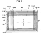
- FIG. 1 is a plan view of the PDP, schematically illustrating an arrangement of electrodes
- FIG. 2 is a perspective view illustrating an image display region of the PDP.
- the numbers of display electrodes, display scan electrodes and address electrodes are reduced to facilitate the description.
- PDP 100 includes front glass substrate 101 (not shown), rear glass substrate 102, N display electrodes 103, N display scan electrodes 104 (the Nth electrode is denoted by N), M address electrodes 107 (the Mth electrode is denoted by M) and hermetically sealing layer 121 designated by a shaded part.
- This PDP 100 has an electrode matrix having a three-electrode structure including electrodes 103, 104, 107. Cells are formed where address electrodes 107 intersect display electrodes 103 and display scan electrodes 104. Image display region 123 is formed inwardly of hermetically sealing layer 121
- PDP 100 is constructed as follows.
- a front panel which includes display electrodes 103, display scan electrodes 104, dielectric glass layer 105 and MgO protective layer 106 disposed above a principal surface of its front glass substrate 101, and a rear panel, which includes address electrodes 107, dielectric glass layer 108, barrier ribs 109 and phosphor layers 110R, 110G, 110B disposed above a principal surface of its rear glass substrate 102, are put together, and discharge space 122 formed between the front and rear panels is filled with discharge gas.
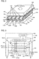
- FIG. 3 is a block diagram illustrating the structure of the plasma display device including a driving circuit.
- PDP 100 is provided with display driver circuit 153, display scan driver circuit 154 and address driver circuit 155. Under control of controller 152, a voltage is applied to display scan electrode 104 and address electrode 107 of the cell to be illuminated for address discharge between these electrodes 104, 107. Thereafter, a pulse voltage is applied between display electrode 103 and display scan electrode 104 for sustain discharge, from which the ultraviolet rays are generated in the above-mentioned cell. Phosphor layer 107 excited by the ultraviolet rays emits the light, thus illuminating the cell. An image is displayed by a combination of the illuminated and unilluminated cells having the respective colors.
- FIG. 4 is a sectional view of the PDP
- FIG. 5 is a sectional view of a phosphor ink applying device.
- the front panel is formed in the following manner. First, N display electrodes 103 and N display scan electrodes 104 (FIG. 2 shows only two electrodes 103 and two electrodes 104) are alternately formed in parallel relation like stripes on front glass substrate 101. Subsequently, these electrodes 103, 104 are covered with dielectric glass layer 105, which is then covered with MgO protective layer 106.
- Display electrode 103 and display scan electrode 104 are each formed of a transparent electrode made of ITO and a bus electrode made of silver and are formed by firing subsequent to application of silver paste for the bus electrodes through screen printing.
- Dielectric glass layer 105 is formed to have a specified thickness (approx. 20 ⁇ m) by applying paste including lead glass material through screen printing and then firing the paste at a specified temperature (e.g. 560°C) for a specified period of time (e.g. 20 minutes).
- a specified temperature e.g. 560°C
- a specified period of time e.g. 20 minutes
- the paste including the lead glass material for use include a mixture of PbO (70 wt%), B 2 O 3 (15 wt%), SiO 2 (10 wt%), Al 2 O 3 (5 wt%), and an organic binder made by dissolving 10% of ethyl cellulose in ⁇ -terpineol.
- the organic binder mentioned here includes resin dissolved in an organic solvent.
- acrylic resin can be used as the resin, and butyl carbitol or the like can be used as the organic solvent.
- a dispersant such as glyceryltriloleate may be mixed into such an organic binder.
- MgO protective layer 106 is made of magnesium oxide (MgO) and is formed by, for example, sputtering or chemical vapor deposition (CVD) to have a specified thickness (about 0.5 ⁇ m).
- the rear panel is formed in the following manner.
- M address electrodes 107 are formed in rows by applying silver paste for these electrodes to rear glass substrate 102 through screen printing or photolithography, and then firing the paste.
- dielectric glass layer 108 is formed on these electrodes 107 by applying paste including lead glass material through screen printing.
- barrier ribs 109 are formed by repeatedly applying the same paste including the lead glass material to dielectric glass layer 108 at specified pitches through screen printing and then firing the paste. These barrier ribs 109 partition discharge space 122 into the cells (unit light-emitting regions) along the rows.
- FIG. 4 is a partially sectional view of PDP 100.
- interval W between barrier ribs 109 is conditioned to range from about 130 ⁇ m to 240 ⁇ m in accordance with a HDTV with a diagonal screen of 32 inches to 50 inches.
- the red (R), green (G) and blue (B) phosphors are each applied to a groove between barrier ribs 109.
- the blue (B) phosphor Ba 1-X MgAl 10 O 17 :Eu X or Ba 1-x-y Sr y MgAl 10 O 17 :Eu X , the pentavalent element is substituted for the part of the Al or Mg element.
- Paste-like phosphor ink including each of these phosphors and an organic binder is applied and fired at a temperature of 400°C to 590°C, whereby the organic binder is burnt out.
- phosphor layers 110R, 110G, 110B each having the phosphor particles bound are formed. It is desirable that thickness L of each of these phosphor layers 110R, 110G, 110B along the direction of lamination be about 8 to 25 times the mean particle diameter of the phosphor particles above address electrode 107. In other words, it is desirable that the phosphor layer has such a thickness that the phosphor particles are stacked to form at least 8 layers, preferably about 20 layers.
- the phosphor layer needs to absorb the ultraviolet rays generated in discharge space 122 for ensuring the luminance (luminous efficiency) when irradiated with a certain amount of ultraviolet rays.
- the luminous efficiency of phosphor layers 110R, 110G, 110B becomes almost saturated.
- a thickness exceeding the thickness of about 20 layers sufficiently large discharge space 122 cannot be secured.
- phosphor particles having sufficiently small particle diameters and spherical shapes, like those obtained by hydrothermal synthesis or the like are packed more densely in a phosphor layer and have a larger total surface area than particles which are not spherical in shape.
- these phosphor particles increase the surface area contributing to actual light emission of the phosphor layer, thus increasing the luminous efficiency. Synthesis methods for these phosphor layers 110R, 110G, 110B, and a method of manufacturing blue phosphor particles including trivalent Eu ions substituting for 15% to 75% of divalent Eu ions for use in a blue phosphor layer are described later.
- the front and rear panels thus made are placed one on top of the other with address electrodes 107 of the rear panel orthogonal to electrodes 103, 104 of the front panel.
- Sealing glass is disposed along a periphery of the panels and fired, for example, at 450°C for 10 to 20 minutes to form hermetically sealing layer 121 (see FIG. 1) for sealing.
- discharge space 122 is once exhausted of air to a high vacuum (e.g. 1.1 ⁇ 10 -4 Pa) and then filled with the discharge gas (e.g. He-Xe or Ne-Xe inert gas) at a specified pressure, thus completing PDP 100.
- a high vacuum e.g. 1.1 ⁇ 10 -4 Pa
- the discharge gas e.g. He-Xe or Ne-Xe inert gas
- FIG. 5 is a schematic diagram illustrating a structure of the ink coating apparatus used in forming the phosphor layer.
- ink coating apparatus 200 includes server 210, pressurizing pump 220 and header 230.
- the phosphor ink is supplied from server 210, which stores the phosphor ink, to header 230.
- Header 230 has ink chamber 230a and nozzle 240 (having an inside diameter of 30 ⁇ m to 120 ⁇ m).
- the phosphor ink supplied to ink chamber 230a by pressurization is discharged continuously from nozzle 240.
- bore diameter D of nozzle 240 be at least 30 ⁇ m to prevent the nozzle from clogging up and at most interval W (ranging from about 130 ⁇ m to 200 ⁇ m) between barrier ribs 109 for preventing the applied ink from extending over the barrier ribs.
- bore diameter D is set at 30 ⁇ m to 130 ⁇ m.
- Header 230 is constructed to be driven linearly by a header scanning mechanism (not shown). Allowing header 230 to scan with nozzle 240 discharging phosphor ink 250 continuously allows the phosphor ink to be applied uniformly to the groove between barrier ribs 109 over rear glass substrate 102.
- the phosphor ink used here has a viscosity kept in a range of 1,500 to 30,000 centipoises (CP) at 25°C.
- Server 210 is provided with an stirring apparatus (not shown), which prevents precipitation of the particles in the phosphor ink by stirring.
- Header 230 is integrally formed to include ink chamber 230a and nozzle 240 and is made by performing machining and electric discharge machining on metallic material.
- the method of forming the phosphor layers is not limited to the method described above.
- Other various kinds of methods usable include photolithography, screen printing and a method of disposing a film including the phosphor particles mixed therein.
- the phosphor particles having each color, the binder and an organic solvent are mixed to form the 1,500- to 30,000-centipoise (CP) phosphor ink.
- CP 1,500- to 30,000-centipoise
- a surface active agent, silica, a dispersant (0.1 to 5 wt%) or the like may be added.
- Ethyl cellulose or acrylic resin can be used as the binder included in the phosphor ink (to account for 0.1 to 10 wt% of the ink), and ⁇ -terpineol or butyl carbitol can be used as the solvent.
- a polymer, such as PMA or PVA, can also be used as the binder, and an organic solvent, such as diethylene glycol or methyl ether, can also be used as the solvent.
- materials including barium nitrate (Ba(NO 3 ) 2 ), magnesium nitrate (Mg(NO 3 ) 2 ), aluminum nitrate (Al(NO 3 ) 3 ) and europium (Eu(NO 3 ) 2 ) are mixed in a molar ratio of 1-X:1:10:X (where 0.03 ⁇ X ⁇ 0.2) and dissolved in an aqueous medium, whereby the hydrated mixed solution is made.
- the aqueous medium ion-exchange water or pure water is preferable because either water contains no impurities.
- the aqueous medium can be used even when a non-aqueous solution, such as methanol or ethanol, is also included.
- a material for substituting the pentavalent ion (Nb, Ta, Pr, P, As, Sb, Bi or Tm) for Mg or Al a nitrate, a chloride or an organic compound that includes the above-mentioned pentavalent ion is used.
- the amount of substitution is as follows. When (Mg 1-a Ma)(Al 1-b Mb) (where M is the pentavalent ion), the material is mixed so that 0.0001 ⁇ a ⁇ 0.03, and 0.0001 ⁇ b ⁇ 0.03.
- the hydrated mixed solution is poured in a container made of corrosion- and heat-resistant material, such as gold or platinum and then undergoes hydrothermal synthesis in a device capable of heating and pressurizing simultaneously, such as the autoclave, for 12 to 20 hours at a specified temperature (100°C to 350°C) under a specified pressure (0.2 MPa to 25MPa), thus forming fine phosphor particles.
- a device capable of heating and pressurizing simultaneously, such as the autoclave, for 12 to 20 hours at a specified temperature (100°C to 350°C) under a specified pressure (0.2 MPa to 25MPa), thus forming fine phosphor particles.
- the particles are fired in a reducing atmosphere (including, for example, 5% of hydrogen and 95% of nitrogen) at a specified temperature (e.g. 1,350°C to 1,600°C) for a specified period of time (e.g. 2 hours) and then classified. Consequently, the desired blue phosphor, Ba 1-x MgAl 10 O 17 :Eu x , including the pentavalent ion substituting for the part of Mg or Al can be obtained.
- this phosphor may be fired in an oxidizing atmosphere (at a temperature of preferably 700°C to 1,000°C).
- the phosphor particles obtained by such hydrothermal synthesis are spherical in shape and have particle diameters smaller than those of particles made by conventional solid-phase reaction (with a mean particle diameter of about 0.05 ⁇ m to 2.0 ⁇ m).
- the term "spherical” used here is defined because most of the phosphor particles have aspect ratios (minor axis diameter/major axis diameter) ranging, for example, between 0.9 and 1.0 inclusive. However, not all the phosphor particles need to have aspect ratios falling within this range.
- the blue phosphor can be obtained even when the hydrated mixed solution prepared in the above-mentioned mixed solution preparation process is sprayed from a nozzle into the high-temperature furnace.
- a resulting mixture is fired at a specified temperature (1,300°C to 1,400°C) for a specified period of time (12 to 20 hours), whereby Ba 1-x-y Sr y MgAl 10 O 17 :Eu x including the pentavalent ion substituting for Mg or Al can be obtained.
- this Ba 1-x-y Sr y MgAl 10 O 17 :Eu x is fired in a reducing atmosphere (including, for example, 5% of hydrogen and 95% of nitrogen) at a specified temperature (1,000°C to 1,600°C) for 2 hours and thereafter classified, whereby the phosphor can be obtained.
- the materials used for the phosphors mainly include the oxide, the nitrate and the hydroxide.
- an organometallic compound including an element such as Ba, Sr, Mg, Al, Eu, Nb, Ta, Pr, P, As, Sb, Bi or Tm, such as a metal alkoxide or acetylacetone, can be used for forming the phosphors. If the above-mentioned reduced phosphor is annealed in an oxidizing atmosphere, a resulting phosphor degrades less from the VUV.
- a mixed solution materials including zinc nitrate (Zn(NO 3 )), silicon nitrate (Si(NO 3 ) 2 ) and manganese nitrate (Mn(NO 3 ) 2 ) are mixed in a molar ratio of 2-X:1:X (where 0.01 ⁇ X ⁇ 0.10).
- this mixed solution is sprayed from a nozzle into the high-temperature furnace heated to 1,500°C with ultrasonic waves applied. In this way, the green phosphor is made.
- a first process of preparing a mixed solution materials including barium nitrate (Ba(NO 3 ) 2 ), aluminum nitrate (Al(NO 3 ) 2 ) and manganese nitrate (Mn(NO 3 ) 2 ) are mixed in a molar ratio of 1-X:12:X (where 0.01 ⁇ X ⁇ 0.10) and then dissolved in ion-exchange water, whereby the mixed solution is made.
- a basic aqueous solution e.g. aqueous ammonia solution
- a hydrate is made.
- this hydrate and ion-exchange water are poured in a capsule made of corrosion- and heat-resistant material, such as platinum or gold and then undergo hydrothermal synthesis in a high-pressure vessel such as the autoclave at a specified temperature (e.g. 100°C to 300°C) under a specified pressure (e.g. 0.2 MPa to 10 MPa) for a specified period of time (e.g. 2 to 20 hours). Thereafter, drying is carried out, whereby desired Ba 1-X Al 12 O 19 :Mn X is obtained.
- a phosphor obtained by this hydrothermal synthesis process has particle diameters of about 0.1 ⁇ m to 2.0 ⁇ m and are spherical in shape. Next, these fine particles are annealed in air at a temperature of 800°C to 1,100°C and then classified, whereby the green phosphor is obtained.
- materials including yttrium nitrate (Y 2 (NO 3 ) 3 ), gadolinium hydronitrate (Gd 2 (NO 3 ) 3 ), boric acid (H 3 BO 3 ) and europium nitrate (Eu 2 (NO 3 ) 3 ) are mixed in a molar ratio of 1-X:2:X (where 0.05 ⁇ X ⁇ 0.20, and the Y-to-Gd ratio is 65:35).
- this mixed solution is heat-treated in air at a temperature of 1,200°C to 1,350°C for 2 hours and then classified, whereby the red phosphor is obtained.
- Y 2-X O 3 :Eu X A description is provided next of the red phosphor, Y 2-X O 3 :Eu X .
- materials including yttorium nitrate (Y 2 (NO 3 ) 2 ) and europium nitrate (Eu(NO 3 ) 2 ) are mixed in a molar ratio of 2-X:X (where 0.05 ⁇ X ⁇ 0.30) and then dissolved in ion-exchange water, whereby the mixed solution is made.
- a basic aqueous solution e.g. aqueous ammonia solution
- a basic aqueous solution e.g. aqueous ammonia solution
- this hydrate and ion-exchange water are poured in a container made of corrosion and heat-resistant material such as platinum or gold and then undergo hydrothermal synthesis in a high-pressure vessel such as the autoclave, for example, at a temperature of 100°C to 300°C under a pressure of 0.2 MPa to 10 MPa for 3 to 12 hours.
- a resulting compound is thereafter dried, whereby fine red phosphor particles are made.
- these phosphor particles are annealed in air at a temperature of 1,300°C to 1,400°C for 2 hours and then classified, whereby the red phosphor is obtained.
- the phosphor obtained by this hydrothermal synthesis process has particle diameters of about 0.1 ⁇ m to 2.0 ⁇ m and are spherical in shape. These particle diameters and shapes are suitable for formation of a phosphor layer having excellent light-emitting characteristics.
- the phosphors used for respective phosphor layers 110R, 110G of above-mentioned PDP 100 are conventional phosphors, while phosphor layer 110B uses the above-mentioned phosphor particles including the pentavalent ion substituting for the part of Mg or Al of the phosphor.
- phosphor layer 110B uses the above-mentioned phosphor particles including the pentavalent ion substituting for the part of Mg or Al of the phosphor.
- the use of the above-mentioned blue phosphor increases the luminance of the blue cell and reduces degradation during panel production, thus eliminating the need for intentional reduction of the luminance of the cells having the other colors. Since the luminances of all the colored cells can thus be used to the full, the luminance of the plasma display device can be increased, while the color temperature of the white display is kept high.
- the blue phosphor of the present invention can find application in a fluorescent lamp where this phosphor emits light in a similar manner by being excited by ultraviolet rays.
- conventional blue phosphor particles to be applied to an inner wall of a fluorescent tube are replaced with the phosphor layer made of the blue phosphor including the pentavalent ion substituting for the part of Mg or Al of the phosphor.
- Application of the present invention to the fluorescent lamp in such a manner can afford luminance and resistance to degradation of the luminance that are more excellent than those of the conventional fluorescent lamp.
- Each plasma display device has a diagonal screen of 42 inches (which is within specifications of a HDTV having a rib pitch of 150 ⁇ m) and was made to include a 20- ⁇ m-thick dielectric glass layer, a 0.5- ⁇ m-thick MgO protective layer and a distance of 0.08 mm between a display electrode and a display scan electrode.
- a discharge space is filled with discharge gas, which is a gas mixture including mainly neon and 5% of xenon gas, at a specified discharge gas pressure.
- a phosphor used as blue phosphor particles used in each of the plasma display devices corresponding to respective samples 1-10 in Table 1 includes a pentavalent ion substituting for a part of Mg or Al of the phosphor.
- Samples 4, 6 and 8 had their respective blue phosphors annealed in an oxidizing atmosphere (including N 2 and O 2 ) at 700°C, 900°C, 1,000°C, respectively, for 2 hours after synthesis.
- Samples 1-4 each use a combination of (Y,Gd) 1-X BO 3 :Eu X (red phosphor), Zn 2-X SiO 4 :Mn X (green phosphor) and Ba 1-X MgAl 10 O 17 :Eu X (blue phosphor).
- Samples 5-10 each use a combination of Y 2-X O 3 :Eu X (red phosphor), Ba 1-X Al 12 O 19 :Mn X (green phosphor) and Ba 1-x-y Sr y MgAl 10 O 17 :Eu X (blue phosphor).
- the conditions of the synthesis method for the phosphor, the pentavalent ion substituting for Mg or Al ion of the blue phosphor, the amount of pentavalent ion, and the substitution ratios of the luminescence centers are varied as shown in Table 1.
- Phosphor ink used for forming a phosphor layer in formation of a PDP uses each of those kinds of phosphor particles shown in Table 1 and was made by mixing the phosphor, resin, a solvent and a dispersant. Each phosphor ink thus made has a viscosity kept in a range of 1,500 CP to 30,000 CP at 25°C. When each phosphor layer formed was observed, the phosphor ink was applied uniformly to each wall surface of each barrier rib.
- the phosphor particles used for the phosphor layer having each color have a mean particle diameter of 0.1 ⁇ m to 3.0 ⁇ m and a maximum particle diameter not more than 8 ⁇ m.
- Comparative sample 11 is a sample using conventional blue phosphor particles which did not undergo any specific substitution.
- Luminance of the blue color of each of samples 1-10 and comparative sample 11 made was measured before as well as after the phosphor was fired (at 520°C for 20 minutes) in a process of manufacturing a rear panel, and a luminance degradation rate of the blue color was determined. Specifically, the luminance of the phosphor particles was measured before firing, and the luminance of the ink applied and fired was measured.
- Luminance was measured before as well as after the PDP was illuminated with blue light, and a luminance degradation rate was determined. Specifically, the luminance of the panel was measured before as well as after discharge sustain pulses of 100 kHz were applied to each plasma display device at 200 V for 100 straight hours, and the luminance degradation rate ( ⁇ [the luminance after the application-the luminance before the application]/the luminance before the application>*100) was determined from these measurements.
- Addressing failure in address discharge was determined by presence of a flicker in an image. Even one flicker is counted as the addressing failure.
- Table 2 shows the luminances and the luminance degradation rates of each color as results of these experiments 1-3.
- comparative sample 11 using the blue phosphor not including the substituent pentavalent ion has a high luminance degradation rate in each step.
- This comparative example 11 has a 5.5 % decrease in luminance after the phosphor firing step, a 21.5 % decrease in luminance after the sealing step and a 35% decrease in luminance in the accelerated life test carried out at 200 V and 100 kHz.
- Samples 1-10 each have a blue color degradation rate lower than 3% and no addressing failure.
- the oxygen vacancies in the blue phosphor were reduced substantially by the substitution of the pentavalent ion (Nb, Ta, Pr, P, As, Sb, Bi or Tm) for the part of the Mg or Al element of the blue phosphor. Accordingly, water existing in the atmosphere or given off by the MgO layer, the barrier rib, the sealing frit, the phosphor and others conceivably did not adsorb on the defective layers (the oxygen vacancies in the vicinity of the Ba-O layers) at the surface of the phosphor in firing of the phosphor and in sealing of the panels.
- Samples 4, 6 and 8 which had their respective blue phosphors annealed in the oxidizing atmosphere, had their oxygen vacancies reduced and accordingly have reduced luminance degradation rates in the test where the discharge sustain pulses of 100 kHz were applied at 200 V.
- these samples were left in an atmosphere having a relative humidity of 90% at 60°C for 10 minutes and then dried at 100°C. Thereafter, these samples underwent temperature-programmed desorption-gas chromatography-mass spectrometry (TDS analysis). As a result, a water physisorption peak (around 100°C) and a water chemisorption peak (300°C to 500°C) of sample 11 which has not undergone the substitution were each ten times as high as the corresponding peak of each of samples 1-10.
- TDS analysis temperature-programmed desorption-gas chromatography-mass spectrometry
- sample fluorescent lamp 12 was made by applying a mixture, including a colored phosphor made under the conditions of sample 7 of Table 1, to an inner wall of a fluorescent tube to form a phosphor layer in a publicly known fluorescent lamp.
- sample fluorescent lamp 13 was made by applying a mixture including the colored phosphor of sample 11 of Table 1 that was made by conventional solid-phase reaction. Table 3 shows results.
- the phosphor of the present invention has a low luminance degradation rate even when used in the fluorescent lamp.
- phosphor layers include a blue phosphor layer.
- This blue phosphor layer is formed of a compound expressed by Ba 1-X MgAl 10 O 17 :Eu X or Ba 1-x-y Sr y MgAl 10 O 17 :Eu X , and at least one element selected from Nb, Ta, Pr, P, As, Sb, Bi and Tm is substituted for a part of an Al or Mg element of this phosphor, so that degradations in various processes for the phosphor layer can be prevented. Consequently, a PDP or a fluorescent lamp can have improved luminance, life and reliability.
Landscapes
- Chemical & Material Sciences (AREA)
- Engineering & Computer Science (AREA)
- Inorganic Chemistry (AREA)
- Materials Engineering (AREA)
- Organic Chemistry (AREA)
- Physics & Mathematics (AREA)
- Plasma & Fusion (AREA)
- Luminescent Compositions (AREA)
- Gas-Filled Discharge Tubes (AREA)
Applications Claiming Priority (3)
| Application Number | Priority Date | Filing Date | Title |
|---|---|---|---|
| JP2002142663 | 2002-05-17 | ||
| JP2002142663A JP4096620B2 (ja) | 2002-05-17 | 2002-05-17 | プラズマディスプレイ装置の製造方法 |
| PCT/JP2003/006049 WO2003097769A1 (en) | 2002-05-17 | 2003-05-15 | Plasma display unit, phosphor and process for producing phosphor |
Publications (2)
| Publication Number | Publication Date |
|---|---|
| EP1512734A1 true EP1512734A1 (de) | 2005-03-09 |
| EP1512734A4 EP1512734A4 (de) | 2007-08-08 |
Family
ID=29544997
Family Applications (1)
| Application Number | Title | Priority Date | Filing Date |
|---|---|---|---|
| EP03730500A Withdrawn EP1512734A4 (de) | 2002-05-17 | 2003-05-15 | Plasmaanzeigegerät, leuchtstoff und verfahren zur herstellung von leuchtstoff |
Country Status (6)
| Country | Link |
|---|---|
| US (1) | US7208102B2 (de) |
| EP (1) | EP1512734A4 (de) |
| JP (1) | JP4096620B2 (de) |
| KR (1) | KR100572782B1 (de) |
| CN (1) | CN100396753C (de) |
| WO (1) | WO2003097769A1 (de) |
Families Citing this family (28)
| Publication number | Priority date | Publication date | Assignee | Title |
|---|---|---|---|---|
| US7009663B2 (en) | 2003-12-17 | 2006-03-07 | Planar Systems, Inc. | Integrated optical light sensitive active matrix liquid crystal display |
| US7053967B2 (en) * | 2002-05-23 | 2006-05-30 | Planar Systems, Inc. | Light sensitive display |
| WO2003073159A1 (en) * | 2002-02-20 | 2003-09-04 | Planar Systems, Inc. | Light sensitive display |
| US20080084374A1 (en) * | 2003-02-20 | 2008-04-10 | Planar Systems, Inc. | Light sensitive display |
| US7285913B2 (en) * | 2003-08-29 | 2007-10-23 | Matsushita Electric Industrial Co., Ltd. | Plasma display device having blue phosphor layers with alkaline earth metal aluminate containing molybdenum or tungsten |
| US7773139B2 (en) | 2004-04-16 | 2010-08-10 | Apple Inc. | Image sensor with photosensitive thin film transistors |
| JP4513397B2 (ja) * | 2004-04-27 | 2010-07-28 | パナソニック株式会社 | プラズマディスプレイ装置 |
| WO2006109694A1 (ja) * | 2005-04-06 | 2006-10-19 | Matsushita Electric Industrial Co., Ltd. | 発光デバイス |
| JPWO2006109681A1 (ja) * | 2005-04-07 | 2008-11-13 | 松下電器産業株式会社 | 発光デバイス |
| KR100759566B1 (ko) * | 2006-01-27 | 2007-09-18 | 삼성에스디아이 주식회사 | 플라즈마 디스플레이 패널과, 이의 제조 방법 |
| KR20090128401A (ko) | 2007-03-01 | 2009-12-15 | 파나소닉 주식회사 | 발광 표시 장치, 플라즈마 표시 장치 및 형광체 입자 |
| JP2010146741A (ja) * | 2008-12-16 | 2010-07-01 | Hitachi Plasma Display Ltd | プラズマディスプレイパネル |
| EP2292719A1 (de) * | 2009-09-04 | 2011-03-09 | Samsung SDI Co., Ltd. | Grüner Phosphor und diesen umfassendes Plasmaanzeigefeld |
| US8017038B2 (en) * | 2009-09-04 | 2011-09-13 | Samsung Sdi Co., Ltd. | Green phosphor and plasma display panel including the same |
| US9310923B2 (en) | 2010-12-03 | 2016-04-12 | Apple Inc. | Input device for touch sensitive devices |
| US9329703B2 (en) | 2011-06-22 | 2016-05-03 | Apple Inc. | Intelligent stylus |
| US8928635B2 (en) | 2011-06-22 | 2015-01-06 | Apple Inc. | Active stylus |
| US8638320B2 (en) | 2011-06-22 | 2014-01-28 | Apple Inc. | Stylus orientation detection |
| CN103930518B (zh) * | 2011-11-24 | 2015-09-16 | 圣戈本陶瓷及塑料股份有限公司 | 发光材料及其形成方法 |
| US9557845B2 (en) | 2012-07-27 | 2017-01-31 | Apple Inc. | Input device for and method of communication with capacitive devices through frequency variation |
| US9652090B2 (en) | 2012-07-27 | 2017-05-16 | Apple Inc. | Device for digital communication through capacitive coupling |
| US9176604B2 (en) | 2012-07-27 | 2015-11-03 | Apple Inc. | Stylus device |
| US10048775B2 (en) | 2013-03-14 | 2018-08-14 | Apple Inc. | Stylus detection and demodulation |
| US10845901B2 (en) | 2013-07-31 | 2020-11-24 | Apple Inc. | Touch controller architecture |
| US10061450B2 (en) | 2014-12-04 | 2018-08-28 | Apple Inc. | Coarse scan and targeted active mode scan for touch |
| JP6288061B2 (ja) * | 2015-12-10 | 2018-03-07 | 日亜化学工業株式会社 | 発光装置の製造方法 |
| US10474277B2 (en) | 2016-05-31 | 2019-11-12 | Apple Inc. | Position-based stylus communication |
| US12153764B1 (en) | 2020-09-25 | 2024-11-26 | Apple Inc. | Stylus with receive architecture for position determination |
Family Cites Families (10)
| Publication number | Priority date | Publication date | Assignee | Title |
|---|---|---|---|---|
| JPH04270782A (ja) * | 1991-02-27 | 1992-09-28 | Toshiba Corp | 蛍光体およびこれを用いた蛍光ランプ |
| KR100247817B1 (ko) * | 1993-02-18 | 2000-03-15 | 손욱 | 형광램프용 청색 발광형광체 |
| TW353678B (en) * | 1994-08-17 | 1999-03-01 | Mitsubishi Chem Corp | Aluminate phosphor |
| JP3405049B2 (ja) * | 1995-05-29 | 2003-05-12 | 日亜化学工業株式会社 | 残光性ランプ |
| DE69824034T2 (de) * | 1997-11-06 | 2005-06-30 | Matsushita Electric Industrial Co., Ltd., Kadoma | Lumineszenzmittel, pulverförmiges lumineszenzmittel, plasma-anzeigetafel und herstellungsverfahren dersleben |
| JP3581800B2 (ja) * | 1999-05-31 | 2004-10-27 | 日立ライティング株式会社 | 蛍光ランプ |
| JP2001055567A (ja) | 1999-08-18 | 2001-02-27 | Fujitsu Ltd | 蛍光体粒子の処理方法及び蛍光体粒子並びにプラズマディスプレイパネル |
| CN1321722A (zh) * | 2000-04-29 | 2001-11-14 | 中国科学院长春光学精密机械与物理研究所 | 一种用于红外光检测的铝酸盐发光材料 |
| JP3755390B2 (ja) * | 2000-09-08 | 2006-03-15 | 株式会社日立製作所 | 蛍光体及びそれを用いた表示装置並びに光源 |
| JP4396016B2 (ja) * | 2000-09-21 | 2010-01-13 | 三菱化学株式会社 | アルミン酸塩蛍光体、蛍光体ペースト組成物及び真空紫外線励起発光装置 |
-
2002
- 2002-05-17 JP JP2002142663A patent/JP4096620B2/ja not_active Expired - Fee Related
-
2003
- 2003-05-15 CN CNB038008882A patent/CN100396753C/zh not_active Expired - Fee Related
- 2003-05-15 EP EP03730500A patent/EP1512734A4/de not_active Withdrawn
- 2003-05-15 WO PCT/JP2003/006049 patent/WO2003097769A1/ja not_active Ceased
- 2003-05-15 US US10/485,305 patent/US7208102B2/en not_active Expired - Fee Related
- 2003-05-15 KR KR1020047002427A patent/KR100572782B1/ko not_active Expired - Fee Related
Also Published As
| Publication number | Publication date |
|---|---|
| US20040183439A1 (en) | 2004-09-23 |
| KR100572782B1 (ko) | 2006-04-24 |
| CN100396753C (zh) | 2008-06-25 |
| JP2003336061A (ja) | 2003-11-28 |
| WO2003097769A1 (en) | 2003-11-27 |
| JP4096620B2 (ja) | 2008-06-04 |
| EP1512734A4 (de) | 2007-08-08 |
| CN1545545A (zh) | 2004-11-10 |
| KR20040027922A (ko) | 2004-04-01 |
| US7208102B2 (en) | 2007-04-24 |
Similar Documents
| Publication | Publication Date | Title |
|---|---|---|
| US7208102B2 (en) | Plasma display unit, phosphor and process for producing phosphor | |
| KR100572432B1 (ko) | 플라즈마 디스플레이 장치, 그에 사용되는 형광체 및 그의 제조 방법 | |
| US6960309B2 (en) | Plasma display apparatus, fluorescent material, and fluorescent material manufacturing method | |
| EP1510566B1 (de) | Leuchtstoff und Plasma-Anzeigevorrichtung | |
| US7204939B2 (en) | Plasma display apparatus, fluorescent material, and fluorescent material manufacturing method | |
| US7288889B2 (en) | Ba-based blue phosphor material provided with a particle surface coating and plasma display panel using the same | |
| JP4244727B2 (ja) | プラズマディスプレイ装置 | |
| US7576487B2 (en) | Plasma display device | |
| KR100572431B1 (ko) | 플라즈마 표시 장치, 형광체 및 형광체의 제조 방법 | |
| US7531961B2 (en) | Plasma display with phosphors containing a β-alumina crystal structure | |
| JP3818285B2 (ja) | プラズマディスプレイ装置 | |
| JP2006059629A (ja) | プラズマディスプレイ装置 | |
| KR100554814B1 (ko) | 청색 형광체, 이의 제조 방법 및 이를 포함하는 플라즈마 디스플레이 장치 | |
| JP4556908B2 (ja) | プラズマディスプレイ装置 | |
| JP2004091623A (ja) | プラズマディスプレイパネル | |
| JP2004067874A (ja) | プラズマディスプレイパネル | |
| JP2005209628A (ja) | プラズマディスプレイ装置およびその製造方法 |
Legal Events
| Date | Code | Title | Description |
|---|---|---|---|
| PUAI | Public reference made under article 153(3) epc to a published international application that has entered the european phase |
Free format text: ORIGINAL CODE: 0009012 |
|
| 17P | Request for examination filed |
Effective date: 20040217 |
|
| AK | Designated contracting states |
Kind code of ref document: A1 Designated state(s): AT BE BG CH CY CZ DE DK EE ES FI FR GB GR HU IE IT LI LU MC NL PT RO SE SI SK TR |
|
| RBV | Designated contracting states (corrected) |
Designated state(s): DE FR GB NL |
|
| A4 | Supplementary search report drawn up and despatched |
Effective date: 20070709 |
|
| 17Q | First examination report despatched |
Effective date: 20071005 |
|
| RAP1 | Party data changed (applicant data changed or rights of an application transferred) |
Owner name: PANASONIC CORPORATION |
|
| STAA | Information on the status of an ep patent application or granted ep patent |
Free format text: STATUS: THE APPLICATION IS DEEMED TO BE WITHDRAWN |
|
| 18D | Application deemed to be withdrawn |
Effective date: 20121204 |