EP1511042B1 - Phasenübergangsspeicheranordnung mit Vorspannung von nicht-selektierten Bit-Leitungen - Google Patents
Phasenübergangsspeicheranordnung mit Vorspannung von nicht-selektierten Bit-Leitungen Download PDFInfo
- Publication number
- EP1511042B1 EP1511042B1 EP03077667A EP03077667A EP1511042B1 EP 1511042 B1 EP1511042 B1 EP 1511042B1 EP 03077667 A EP03077667 A EP 03077667A EP 03077667 A EP03077667 A EP 03077667A EP 1511042 B1 EP1511042 B1 EP 1511042B1
- Authority
- EP
- European Patent Office
- Prior art keywords
- bit line
- bit lines
- biasing
- memory device
- deselected
- Prior art date
- Legal status (The legal status is an assumption and is not a legal conclusion. Google has not performed a legal analysis and makes no representation as to the accuracy of the status listed.)
- Expired - Lifetime
Links
- 239000011159 matrix material Substances 0.000 claims description 14
- 238000007599 discharging Methods 0.000 claims description 9
- 230000008859 change Effects 0.000 claims description 6
- 238000000034 method Methods 0.000 claims description 6
- 239000003990 capacitor Substances 0.000 description 14
- 239000000463 material Substances 0.000 description 14
- 230000004044 response Effects 0.000 description 8
- 239000012782 phase change material Substances 0.000 description 5
- 230000000694 effects Effects 0.000 description 2
- 238000011084 recovery Methods 0.000 description 2
- 230000001052 transient effect Effects 0.000 description 2
- 239000000956 alloy Substances 0.000 description 1
- 229910045601 alloy Inorganic materials 0.000 description 1
- 230000004075 alteration Effects 0.000 description 1
- 238000013500 data storage Methods 0.000 description 1
- 238000010586 diagram Methods 0.000 description 1
- 238000010438 heat treatment Methods 0.000 description 1
- 230000002452 interceptive effect Effects 0.000 description 1
- 230000008018 melting Effects 0.000 description 1
- 238000002844 melting Methods 0.000 description 1
- 238000012986 modification Methods 0.000 description 1
- 230000004048 modification Effects 0.000 description 1
- 230000006911 nucleation Effects 0.000 description 1
- 238000010899 nucleation Methods 0.000 description 1
- 230000008569 process Effects 0.000 description 1
- 230000000630 rising effect Effects 0.000 description 1
Images


Classifications
-
- G—PHYSICS
- G11—INFORMATION STORAGE
- G11C—STATIC STORES
- G11C7/00—Arrangements for writing information into, or reading information out from, a digital store
- G11C7/12—Bit line control circuits, e.g. drivers, boosters, pull-up circuits, pull-down circuits, precharging circuits, equalising circuits, for bit lines
-
- G—PHYSICS
- G11—INFORMATION STORAGE
- G11C—STATIC STORES
- G11C13/00—Digital stores characterised by the use of storage elements not covered by groups G11C11/00, G11C23/00, or G11C25/00
- G11C13/0002—Digital stores characterised by the use of storage elements not covered by groups G11C11/00, G11C23/00, or G11C25/00 using resistive RAM [RRAM] elements
- G11C13/0004—Digital stores characterised by the use of storage elements not covered by groups G11C11/00, G11C23/00, or G11C25/00 using resistive RAM [RRAM] elements comprising amorphous/crystalline phase transition cells
-
- G—PHYSICS
- G11—INFORMATION STORAGE
- G11C—STATIC STORES
- G11C13/00—Digital stores characterised by the use of storage elements not covered by groups G11C11/00, G11C23/00, or G11C25/00
- G11C13/0002—Digital stores characterised by the use of storage elements not covered by groups G11C11/00, G11C23/00, or G11C25/00 using resistive RAM [RRAM] elements
- G11C13/0021—Auxiliary circuits
- G11C13/0023—Address circuits or decoders
- G11C13/0026—Bit-line or column circuits
-
- G—PHYSICS
- G11—INFORMATION STORAGE
- G11C—STATIC STORES
- G11C2213/00—Indexing scheme relating to G11C13/00 for features not covered by this group
- G11C2213/70—Resistive array aspects
- G11C2213/79—Array wherein the access device being a transistor
Definitions
- the present invention relates to the data storage field, and more specifically to a memory device.
- phase-change E 2 PROM is a non-volatile memory exploiting the properties of a material that can be reversibly switched between an amorphous phase and a crystalline phase.
- the phase-change material exhibits different electrical characteristics depending on its phase, each one representing a corresponding logic value.
- An example of a phase-change E 2 PROM is described in US-A-5,166,758 .
- the memory device includes a matrix of memory cells, each one consisting of a functional element connected in series to an access element (such as the base-emitter junction of a bipolar transistor).
- the memory cells are arranged between corresponding word lines and bit lines.
- the word lines are kept at high voltage, so that all the access elements are reverse biased.
- a leakage current flows through each access element; for this reason, the bit lines are generally connected to a terminal providing a reference voltage, in order to avoid charging a stray capacitor associated with each bit line to a dangerous voltage.
- bit lines are disconnected from the reference terminal.
- the voltage on a selected word line is then lowered, and one or more selected bit lines are driven to a voltage corresponding to the operation to be performed (while the other bit lines are left floating). In this condition, the access elements associated with the selected word line and the selected bit lines are forward biased.
- a drawback of the solution described above is that the leakage currents in each deselected bit line charge the corresponding stray capacitor. The voltage reached on the deselected bit line can turn on the access element associated with the selected word line.
- phase switch can cause an undesired change of the value stored in the memory cell. In any case, even when the phase switch is only transient, a wrong value can be read if the memory cell is selected before a corresponding recovery time.
- the problem is exacerbated when the temperature increases, since the leakage current typically depends on the temperature according to an exponential law.
- the total leakage current injected into each functional element in the selected word line is directly proportional to the number of access elements in the corresponding deselected bit line.
- WO-A-02/058632 proposes applying bias signals to the unselected memory cells during the reading or programming; the voltage potential of these bias signals is selected so as to not disturb the stored data.
- US 6404666 B1 concerns a read only memory in which, it is claimed, effects of "off" state leakage current of non-selected memory cells are eliminated in order to prevent read errors.
- the ROM comprises word lines WL1-n activated in response to an address signal, sense lines CL1-m intersected with the word lines WL1-n and selected in response to a selection signal SL1-m,r, a reference sense line CLr intersected with the word lines WL1-n, memory cells 1m,n storing data therein, reference memory cells 51-n connected to the reference sense line CLr, a sense amplifier 9 for comparing currents flowing on the selected one of the sense lines CL1-n and on the reference sense line CLr.
- the ROM further comprises a correction current supply circuit 40 connected to the sense lines CL1-n and the reference sense line CLr.
- the correction current supply circuit 40 generates a correction current approximately corresponding to a leakage current flowing through the memory cells 1m,n connected to the selected one of the sense lines CL1-n and provides the correction current to the sense lines CL1-n and the reference sense line CLr.
- the present invention also provides corresponding methods of operating a memory device as set out independent claims 9 and 10.
- a memory device 100 consisting of an E 2 PROM of the phase-change type, is shown.
- Each programmable element P h,k is made of a phase-change material; typically, the phase-change material consists of a calcogenide (such as an alloy Ge 2 Sb 2 Te 5 ).
- the phase-change material can be reversibly switched between a generally amorphous, disordered phase and a generally crystalline, high ordered phase.
- the two phases of the material exhibit different electrical characteristics; particularly, the material in the amorphous phase has a high resistivity (defining a reset state associated with a first logic value, for example, 0), whereas the material in the crystalline phase has a low resistivity (defining a set state associated with a second logic value, for example, 1).
- the phase of the material is stable below a predefined temperature (such as 150°C).
- the phase can be changed by heating the material over that temperature.
- a voltage higher than a corresponding phase-change value Vpc (for example, 0.6V) is applied to the programmable element P h,k ; the voltage causes a current to flow through a resistive element (or heater) in contact with the phase-change material, which element heats by the Joule effect and then raises the temperature of the change-phase material accordingly.
- the change-phase material becomes crystalline; conversely, if the programmable element P h,k is brought over a higher melting temperature (such as 600°C) and then cooled rapidly, the change-phase material becomes amorphous.
- the state of the programmable element P h,k is detected by applying a reading voltage (lower than the phase-change value Vpc, so as not to affect the phase of the material).
- the resulting current flowing through the programmable element P h,k is a signature of the resistivity of the material and then of its phase.
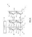
- Each memory cell P h,k -T h,k is connected between a word line WL h and a bit line BL k . More specifically, the programmable elements P h,k of each column have a first terminal connected to the corresponding bit line BL k . A second terminal of each programmable element P h,k is connected to the emitter terminal of the respective access transistor T h,k .
- the access transistors T h,k of each row have the base terminal connected to the corresponding word line WL h ; the collector terminals of all the access transistors T h,k are connected to a ground terminal. In this way, each couple word line/bit line (WL h /BL k ) addresses a single memory cell P h,k -T h,k of the matrix 105.
- the memory device 100 simultaneously processes a word (for example, consisting of 16 bits).
- the bits of each word are stored in memory cells P h,k -T h,k associated with a single word line WL h ; the bit lines BL k of the matrix 105 are grouped into 16 sub-sets, each one for a bit of the different words.
- Each word is identified by an address ADR; in the following, the elements selected by the address ADR will be differentiated adding the sing "'" to the corresponding indexes.
- the address ADR consists of a portion ROW_ADR that is provided to a row decoder 110r and a portion COL_ADR that is provided to a column decoder 110c.
- the row decoder 110r selects the word line WL h , of the desired word.
- the column decoder 110c drives a multiplexer 115, which selects a bit line BL k , of the word in each sub-set.
- the multiplexer 115 interfaces with a read/write unit 120; the read/write unit 120 includes all the components (such as sense amplifiers, comparators, charge pumps, reference cells, pulse generators, and the like), which are used to write the selected programmable elements P h',k' or to read their values.
- the read/write unit 120 includes all the components (such as sense amplifiers, comparators, charge pumps, reference cells, pulse generators, and the like), which are used to write the selected programmable elements P h',k' or to read their values.
- Each bit line BL k is further connected to a discharge transistor D k (consisting of an NMOS).
- the discharge transistor D k has the drain terminal connected to the corresponding bit line BL k , and the source terminal connected to a terminal providing a reference voltage (for example, the ground terminal).
- the gate terminals of all the transistors D k are controlled by a discharge signal DIS.
- all the word lines WL h are kept at a high disabling voltage Vh (for example, 4.5V), while all the bit lines BL k are disconnected from the read/write unit 120.
- the discharge signal DIS is asserted at a power supply voltage Vdd of the memory device (for example, 1.8V); therefore, all the discharge transistors D k are on. In this way, the base-emitter junctions of all the access transistors T h,k are reverse biased (so as to disconnect the programmable elements P h,k from the corresponding word lines WL h ). However, a small leakage current Io flows through each access transistor T h,k .
- the leakage currents Io of the access transistors T h,k associated with each bit line BL k are drained to the ground terminal by means of the corresponding discharge transistor D k . This avoids charging a stray capacitor C k associated with the bit line BL k (shown in thin lines in the figure) to a dangerous voltage.
- the discharge signal DIS is deasserted at the ground voltage (0V), so that all the discharge transistors D k turn off.
- the selected word line WL h' is then brought to a low enabling voltage Vl (for example, 0V).
- Vl for example, 0V.
- the selected bit lines BL k' are connected to the read/write unit 120 (while the other bit lines BL k are left floating); the read/write unit 120 drives the selected bit lines BL k' to a voltage corresponding to the requested operation.
- Vbe base-emitter threshold voltage
- a high voltage pulse is applied to each selected bit line BL k' ; the voltage pulse has an amplitude and a duration depending on the desired state of the corresponding programmable element P h',k' .
- a low voltage for example, IV is applied to the selected bit lines BL k' .
- the current flowing through each corresponding programmable element P h',k' is compared with a threshold value (typically provided by a reference cell); when the programmable element P h',k' is in the crystalline state a current higher than the threshold value is detected (corresponding to the logic value 1), whereas when the programmable element P h',k' is in the amorphous state a current lower than the threshold value is detected (corresponding to the logic value 0).
- a threshold value typically provided by a reference cell
- phase-charge value Vpc 0.6V
- a switch of the phase of the material can occur.
- the phase switch can cause a spurious set of the state of the programmable element P h',k (from the amorphous phase to the crystalline phase), with an undesired change of the stored value.
- a wrong value can be read if the programmable element P h',k is selected before a corresponding recovery time.
- the worst condition wherein the programmable element P h',k associated with the selected word line WL h' is in the amorphous state, for example, with a resistance of 1M ⁇
- the memory device has a different structure, if the memory cells are multilevel, or if the operative parameters of the memory device have other values.
- the memory cells are arranged in two or more matrixes, a different number of bit lines is selected simultaneously (down to a single one), or the BJT transistors are replaced with equivalent unidirectional conduction access elements (such as diodes or MOS transistors).
- FIG. 2 a memory device 200 according to a first embodiment of the invention is illustrated (the elements corresponding to the ones in the Figure 1a are denoted with the same references, and their explanation is omitted for the sake of simplicity).
- the memory device 200 includes one or more auxiliary (or dummy) columns of memory cells Pd h -Td h (only one shown in the figure); preferably, a dummy column of memory cells Pd h -Td h is provided for each sub-set of bit lines BL k (so as to reduce any mismatching).
- Each memory cell Pd h -Td h consists of the series of a programmable element Pd h and an access transistor Td h .
- the memory cells Pd h -Td h of the dummy column are associated with a dummy bit line BLd, which is coupled with the multiplexer 115.
- the dummy bit line BLd has a capacitance represented by a stray capacitor Cd (shown in thin lines in the figure).
- Each memory cell Pd h -Td h is connected between a word line WL h and the dummy bit line BLd. More specifically, all the programmable elements Pd h have a first terminal connected to the dummy bit line BLd. A second terminal of each programmable element Pd h is connected to the emitter terminal of the respective access transistor Td h . Each access transistor Td h has the base terminal connected to the corresponding word line WL h ; the collector terminals of all the access transistors Td h are connected to the ground terminal.
- Each (functional) bit line BL k is connected to the drain terminal of a stand-by transistor S k (consisting of an NMOS); likewise, the dummy bit line BLd is connected to the drain terminal of a stand-by transistor Sd.
- the gate terminals of all the transistors S k ,Sd are controlled by a stand-by signal SB; the stand-by signal SB is underlined to indicate that it is asserted at low voltage (0V) and asserted at high voltage (Vdd).
- each stand-by transistor S k is connected to the drain terminal of a biasing transistor B k (consisting of an NMOS), and the source terminal of the stand-by transistor Sd is connected to the drain terminal of a biasing transistor Bd.
- the biasing transistors B k ,Bd have a natural structure (without any specific doping of their channel regions); therefore, the biasing transistors B k ,Bd exhibit a very low gate-source threshold voltage (such as 0.3V).
- the source terminals of all the biasing transistors B k ,Bd are connected to the ground terminal.
- the gate terminal of the biasing transistor Bd is short-circuited to the drain terminal of the stand-by transistor Sd.
- the gate terminal of the biasing transistor Bd is also connected to the gate terminals of all the biasing transistors B k through a buffer 205.
- the buffer 205 consists of an operational amplifier in the follower configuration (with the inverting input terminal short-circuited to its output terminal).
- the gate terminal of the biasing transistor Bd is connected to the non-inverting input terminal of the buffer 205.
- the output terminal of the buffer 205 directly drives the gate terminals of all the biasing transistors B k .
- the structure B k ,Bd,205 implements a (buffered) current mirror.
- the buffer 205 decouples the input leg from the output legs, providing the current capability required to drive the high capacitive load of the gate terminals of all the biasing transistors B k .
- the stand-by signal SB is deasserted (Vdd) when the memory device 200 is in use; in response thereto, the transistors S k ,Sd turn on. In this condition, the voltage on every bit line BL k ,BLd (disregarding the small overdrive of the biasing transistors B k ,Bd) is kept at the gate-source threshold voltage of the biasing transistor Bd (0.3V).
- the voltage on the selected bit lines BL k' is driven to the desired value by the read/write unit 120; it should be noted that the above described structure does not interfere with operation of the memory device 200 (being the driving capability of the read/write unit 120 far higher than the one of the biasing transistors B k' ). Moreover, the selected bit lines BL k' are already at a positive voltage (0.3V) at the beginning of the operation. Therefore, the speed of the operation is increased (since it is not necessary to charge the selected bit lines BL k' to the desired voltage from ground); at the same time, the power consumption of the memory device 200 is reduced accordingly.
- the other bit lines BL k ,BLd are always maintained at the gate-source threshold voltage of the biasing transistor Bd.
- the low threshold voltage of the biasing transistors B k ,Bd provides a good safety margin (since the voltage on the deselected bit lines BL k is far away from its dangerous value); at the same time, the stand-by transistors S k ,Sd ensure a complete cut off of the current flowing through the bit lines BL k ,BLd in the deep stand-by condition (which complete cut off cannot be guaranteed by the intrinsic characteristics of the biasing transistors B k ,Bd).
- the current mirror B k ,Bd,205 drains the current provided by the dummy bit line BLd towards the ground terminal in each functional bit line BL k .
- the drained current is substantially the same as the total leakage currents Io in each deselected bit line BL k (being the voltage applied to the respective access transistors T h,k exactly the same); that current is also very similar to the total leakage current Io in the selected bit line BL k' , since the difference due to the (forward biased) access transistor T h',k' in the selected word line WL h' is negligible.
- any noise in the value of the current that is detected by the read/write unit 120 (owing to the leakage currents Io flowing through the selected bit line BL k' ) is substantially reduced.
- the current that is driven in the selected bit line BL k' by the read/write unit 120 may be higher (without the risk of switching the phase of the material, because of an increase of the current flowing through the programmable element P h',k' due to the leakage currents Io).
- the concepts of the present inventions are also applicable when the gate terminal of each biasing transistor is short-circuited to its drain terminal, when the positions of the stand-by transistors and the biasing transistors are reversed, or when the stand-by transistors are replaced with equivalent electronic switches.
- the current mirror can be implemented without any buffer, the biasing transistors can be non-natural (for example, they consist of standard transistors modeled with a lower threshold voltage), or a single dummy bit line can be used for the whole matrix.
- FIG. 3a A different embodiment of the invention is illustrated in Figure 3a (the elements corresponding to the ones in the Figures 1a and 2 are denoted with the same references, and their explanation is omitted for the sake of simplicity).
- the figure shows a memory device 300a, wherein the matrix 105 includes the (functional) bit lines BL k with the respective discharge transistors D k .
- the memory device 300a further includes a dummy column of memory cells Pd h -Td h for each sub-set of bit lines BL k .
- the dummy bit line BLd is connected to an additional discharge transistor Dd.
- the discharge transistor Dd has the drain terminal connected to the dummy bit line BLd and the source terminal connected to the ground terminal; the gate terminal of the transistor Dd is controlled by the discharge signal DIS.
- the discharge signal DIS for all the transistors D k ,Dd is generated by an internal logic circuit 303 (as described in detail in the following).
- a reference block 305h (for example, consisting of a band-gap circuit) generates an upper threshold voltage Vth u (such as 0.5V).
- the upper threshold voltage Vth u is supplied to the inverting input terminal of a comparator 310h; the non-inverting input terminal of the comparator 310h is directly connected to the dummy bit line BLd.
- the output terminal of the comparator 310h supplies a signal START to the logic block 303; the signal START is asserted when the voltage on the dummy bit line BLd exceeds the upper threshold voltage Vth u .
- a further reference block 3051 generates a lower threshold voltage Vth 1 (such as 0.3V).
- the lower threshold voltage Vth 1 is supplied to the non-inverting input terminal of a comparator 3101; the inverting input terminal of the comparator 3101 is directly connected to the dummy bit line BLd.
- the output terminal of the comparator 3101 supplies a signal STOP to the logic block 303; the signal STOP is asserted when the voltage on the dummy bit line BLd falls below the lower threshold voltage Vth 1 .
- the logic block 303 asserts and deasserts the discharge signal DIS in response to the signal START and to the signal STOP, respectively.
- the logic block 303 consists of a latch that is set by the signal START and is reset by the signal STOP.
- the leakage currents Io flowing through the access transistors Td h of the dummy bit line BLd charge the corresponding stray capacitor Cd.
- the same considerations apply to all the functional bit lines BL k in the stand-by condition or to the deselected bit lines BL k when a reading/writing operation is in progress (while the selected bit line BL k' is driven to the desired voltage by the read/write unit 120).
- the voltage on the dummy bit line BLd is substantially the same as the voltage on each deselected bit line BL k ; in this way, it is possible to obtain a measure of the voltage on the deselected bit lines BL k without updating the structure of the matrix 105; moreover, this solution avoids interfering with operation of the memory device 300a (for example, because of the capacitive loads of the comparators 310h and 310l).
- the signal START is asserted.
- the discharge signal DIS is asserted as well, so that all the discharge transistors D k ,Dd turn on.
- the voltage on the deselected bit lines BL k and on the dummy bit line BLd are pulled down (with the leakage currents Io that are drained towards the ground terminal through the respective discharge transistors D k ,Dd); the signal START is then deasserted after a short delay. It should be noted that the above-described structure does not interfere with operation of the memory device 300a (being the driving capability of the read/write unit 120 far higher than the one of the discharge transistors D k ).
- the signal STOP is asserted.
- the discharge signal DIS is deasserted, so that all the discharge transistors D k ,Dd turn off.
- the stray capacitor Cd of the dummy bit line BLd and the stray capacitors C k of the deselected bit lines BL k start charging again (with the signal STOP that is deasserted after a short delay).
- each deselected bit line BL k (and on the dummy bit line BLd at the same time) is maintained in a range defined by the lower threshold voltage Vth 1 and the upper threshold voltage Vth u .
- the proposed solution prevents the voltage on the deselected bit lines BL k from reaching a dangerous value. At the same time, the bit lines BL k are maintained at a voltage that improves the speed of any operation on the memory device 300a and reduces its power consumption.
- FIG. 3b An alternative implementation of the structure described above is illustrated in Figure 3b (the elements corresponding to the ones in the Figure 3a are denoted with the same references, and their explanation is omitted for the sake of simplicity).
- the figure shows a memory device 300b, wherein the discharge signal DIS is obtained from the signal START only (without the blocks for generating the signal STOP).
- the signal START is provided to a delay line 320.
- the delay line 320 asserts the discharge signal DIS in response to the assertion of the signal START; the discharge signal DIS is maintained asserted for a pre-set period (for example, some ms).
- the leakage currents Io flowing through the access transistors Td h ,T h,k of the dummy bit line BLd and the deselected bit lines BL k charge the respective stray capacitors Cd,C k .
- the signal START is asserted.
- the discharge signal DIS is asserted as well, so that all the discharge transistors D k , Dd turn on.
- the stray capacitors C k associated with the deselected bit lines BL k and the stray capacitor Cd associated with the dummy bit line BLd are discharged towards the ground terminal; the signal START is then deasserted after a short delay.
- the voltage on the deselected bit lines BL k and on the dummy bit line BLd are reduced of a value corresponding to the duration of the discharge signal DIS (for example, a few hundreds of mV).
- the discharge signal DIS is deasserted, all the discharge transistors D k ,Dd turn off.
- the stray capacitors C k ,Cd of the deselected bit lines BL k and of the dummy bit line BLd then start charging again.
- each deselected bit line BL k (and on the dummy bit line BLd at the same time) is maintained in a predefined range having its upper limit defined by the voltage Vth u .
- an aspect of the present invention proposes a memory device.
- the memory device includes a matrix of memory cells, which are arranged in a plurality of rows and a plurality of columns; each memory cell includes a functional element with a programmable resistivity and a unidirectional conduction access element connected in series.
- the memory device further includes a plurality of word lines and a plurality of bit lines; the memory cells of each row are connected to a corresponding word line and the memory cells of each column are connected to a corresponding bit line.
- Means are provided for driving the bit lines to a desired voltage.
- Means are used for selecting one or more bit lines in an operative condition of the memory device; each selected bit line is connected to the means for driving and each deselected bit line is disconnected from the means for driving.
- each access element associated with the selected word line and the selected bit lines is forward biased and the other access elements are reverse biased.
- the memory device of the invention further includes means for biasing the deselected bit lines in the operative condition, in order to prevent a leakage current of the reverse biased access elements from forward biasing the access elements associated with the selected word line and the deselected bit lines.
- the biasing of the deselected bit lines in the operative condition ensures that the leakage currents do not charge the corresponding stray capacitors over a dangerous voltage.
- the devised structure avoids turning on the access elements (in the deselected bit lines) that are associated with the selected word line. As a consequence, any wrong reading of the memory cells or any undesired change in their state is prevented.
- the solution of the invention is particularly advantageous when the memory device works at high temperature or when the matrix of memory cells includes a high number of rows (even if different applications are not excluded).
- a biasing current (corresponding to the total leakage current in each deselected bit line) is continuously drained from all the bit lines.
- This solution reduces the voltage that can be reached by the bit lines; at the same time, the current drained from the selected bit line improves the precision of the reading operations.
- a suggested choice for implementing the above-described structure is that of using a dummy column of memory cells (providing a current that is mirrored to every functional bit line).
- the current that is drained from each bit line is substantially the same as the corresponding total leakage current.
- the biasing transistors have a low threshold voltage, and additional electronic switches are used to disconnect the bit lines from the current mirror in the stand-by condition.
- the solution according to the present invention leads itself to be implemented draining the biasing current from the deselected bit lines in a different way, or with another structure for generating the current to be drained; alternatively, the threshold voltage of the biasing transistors is the same as the one of the access transistors, or the memory device does not include any stand-by transistor.
- the stand-by condition can be entered applying a negative voltage (such as -0.1V) to the biasing transistors; in this way, a complete cut off of the current flowing through the bit lines is achieved without any additional stand-by transistors.
- bit lines are discharged when their voltage reaches a threshold value.
- the voltage on the deselected bit lines is prevented from rising over a dangerous value; at the same time, the voltage maintained on the bit lines improves the speed of any operation on the memory device and reduces its power consumption.
- the proposed solution does not require any stand-by circuit.
- the voltage on the deselected bit lines is estimated using a dummy column of memory cells.
- the devised structure avoids updating the matrix of memory cells, and does not introduce any additional capacitive load on the functional bit lines.
- the discharging of the bit lines is stopped when their voltage falls below a further threshold value.
- the voltage on the deselected bit lines can be maintained in a predefined range with a high degree of precision.
- a different implementation involves the discharging of the bit lines for a predefined period.
- the voltage on the bit lines is measured directly (without any dummy column of memory cells), or the discharging of the bit lines is enabled in a different way.
- the bit lines can be discharged periodically (even if a discharge frequency working correctly at the highest temperature that is allowable for the memory device involves an increase in the power consumption at room temperature).
- the solution of the invention is also suitable to be implemented with different structures for biasing the bit lines (or at least the deselected ones) in the operative condition of the memory device.
- the solution of the invention is specifically designed for a phase-change memory device (even if different applications are not excluded).
Landscapes
- Chemical & Material Sciences (AREA)
- Crystallography & Structural Chemistry (AREA)
- Read Only Memory (AREA)
Claims (10)
- Speichervorrichtung (300a, 300b) mit einer Matrix (105) von Speicherzellen (Ph,k, Th,k), die in mehreren Reihen und mehreren Spalten angeordnet sind, wobei jede Speicherzelle Folgendes umfasst: ein Funktionselement (Ph,k) mit einem programmierbaren spezifischen Widerstand und einem in Serie geschalteten unidirektionalen Leitungszugangselement (Th,k), mehrere Wortleitungen (WLh) und mehrere Bitleitungen (BLk), wobei die Speicherzellen jeder Reihe mit einer entsprechenden Wortleitung verbunden sind und die Speicherzellen jeder Spalte mit einer entsprechenden Bitleitung verbunden sind, Bitleitungsansteuerungsmittel (120) zum Ansteuern der Bitleitungen auf eine gewünschte Spannung, Bitleitungsauswahlmittel (110c, 115) zum Auswählen von wenigstens einer Bitleitung in einen Betriebszustand der Speichervorrichtung, wobei jede ausgewählte Bitleitung mit dem Bitleitungsansteuerungsmittel verbunden ist und jede abgewählte Bitleitung von dem Bitleitungsansteuerungsmittel abgetrennt wird, Wortleitungsauswahlmittel (110r) zum Auswählen einer Wortleitung im Betriebszustand, wobei jedes mit der gewählten Wortleitung und der wenigstens einen gewählten Bitleitung verbundene Zugangselement in Vorwärtsrichtung vorgespannt ist und die anderen Zugangselemente in Rückwärtsrichtung vorgespannt sind, und
Bitleitungsvorspannmittel (Pdh, Tdh; Dk, Dd, 303-320) zum Vorspannen der angewählten Bitleitungen im Betriebszustand der Speichervorrichtung, um zu verhindern, dass ein Leckstrom der in Rückwärtsrichtung vorgespannten Zugangselemente die mit der gewählten Wortleitung und den abgewählten Bitleitungen assoziierten Zugangseleinente in Vorwärtsrichtung vorspannen, wobei die Bitleitungen (BLk) zu Teilsätzen gruppiert sind,
dadurch gekennzeichnet, dass
das Bitleitungsvorspannmittel (Pdh, Tdh; BLd; Dk, Dd, 303-320) eine Vorspannstruktur für jeden Teilsatz beinhaltet, wobei die Vorspannstruktur Bitleitungsentladungsmittel (Dk, Dd) zum Entladen der entsprechenden Bitleitungen und Freigabemittel (303-320) zum Freigeben des Bitleitungsentladungsmittels beinhaltet, wenn ein Spannungswert, der eine Spannung auf den entsprechenden abgewählten Bitleitungen anzeigt, einen Schwellenwert erreicht. - Speichervorrichtung (300a, 300b) nach Anspruch 1, wobei jede Vorspannungsstruktur ferner eine Zusatzspalte von Speicherzellen (Pdh, Tdh) beinhaltet, wobei die Speicherzellen der Zusatzspalte mit einer Zusatzbitleitung (BLd) assoziiert sind, die von dem Bitleitungsansteuerungsmittel (120) im Betriebszustand der Speichervorrichtung abgetrennt ist, und wobei die Anzeige der Spannung auf entsprechenden angewählten Bitleitungen aus einer Spannung auf der Zusatzbitleitung besteht.
- Speichervorrichtung (300a, 300b) nach Anspruch 1 oder 2, wobei jede Vorspannungsstruktur (Pdh, Tdh, Dk, Dd, 303-320) ferner Sperrmittel (3051, 3101) zum Sperren des Bitleitungsentladnngstnittels (Dk, Dd) beinhaltet, wenn der Spannungswert, der eine Spannung auf den entsprechenden angewählten Bitleitungen anzeigt, einen durch den Schwellenwert und einen weiteren Schwellenwert definierten Bereich verlässt.
- Speichervorrichtung (300a, 300b) nach Anspruch 1 oder 2, wobei jede Vorspannungsstruktur ferner Mittel (320) zum Sperren des Bitleitungsentladungsmittels (Dk, Dd) nach einer vorbestimmten Verzögerung nach deren Freigabe beinhaltet.
- Speichervorrichtung (200) mit einer Matrix (105) von Speicherzellen (Ph,k, Th,k), die in mehreren Reihen und mehreren Spalten angeordnet sind, wobei jede Speicherzelle Folgendes beinhaltet: ein Funktionselement (Ph,k) mit einem programmierbaren spezifischen Widerstand und einem in Serie geschalteten unidirektionalen Leitungszugangselement (Th,k), mehrere Wortleitungen (WLh) und mehrere Bitleitungen (BLk), wobei die Speicherzellen jeder Reihe mit einer entsprechenden Wortleitung verbunden sind und die Speicherzellen jeder Spalte mit einer entsprechenden Bitleitung verbunden sind, Bitleitungsansteuerungsmittel (120) zum Ansteuern der Bitleitungen auf eine gewünschte Spannung, Bitleitungsauswahlmittel (110c, 115) zum Auswählen von wenigstens einer Bitleitung in einem Betriebszustand der Speichervorrichtung, wobei jede gewählte Bitleitung mit dem Bitleitungsansteuerungsmittel verbunden ist und jede abgewählte Bitleitung von dem Bitleitungsansteuerungsmittel abgetrennt wird, Wortleitungsauswahtmittel (110r) zum Auswählen einer Wortleitung im Betriebszustand der Speichervorrichtung, wobei jedes mit der gewählten Wortleitung und der wenigstens einen gewählten Bitleitung verbundene Zugangselement in Vorwärtsrichtung vorgespannt ist und die anderen Zugangselemente in Rückwärtsrichtung vorgespannt sind, und
Bitleitungsvorspaiinmittel (Pdh, Tdh; Bk, Bd, 205, Sk, Sd) zum Vorspannen der abgewählten Bitleitungen im Betriebszustand, um zu verhindern, dass ein Leckstrom der in Rückwärtsrichtung vorgespannten Zugangselemente die mit der gewählten Wortleitung und den abgewählten Bitleitungen assoziierten Zugangseleniente in Vorwärtsrichtung vorspannen, wobei die Bitleitungen (BLk) zu Teilsätzen gruppiert sind,
dadurch gekennzeichnet, dass
das Bitleitungsvorspannmittel (Pdh, Tdh; Bk, Bd, 205, Sk, Sd) eine Vorspannstruktur für jeden Teilsatz beinhaltet, wobei die Vorspannstruktur Mittel (Pdh, Tdh) zum Zuführen eines Vorspannungsstroms beinhaltet, die einem Gesamtleckstrom jeder Bitleitung des Teilsatzes entspricht, und Drain-Mittel (Bk, Bd, 205) zum Abführen des Vorspannungsstroms von allen Bitleitungen des Teilsatzes, wobei das Drain-mittel ferner zum Vermeiden des Einschaltens der Zugangselemente in den abgewählten Bitleitungen konfiguriert ist, die mit der gewählten Wortleitung assoziiert sind, um dadurch falsches Lesen der Speicherzellen aufgrund einer unerwünschten Veränderung eines Zustands des programmierbaren spezifischen Widerstands der Funktionselemente zu verhindern. - Speichervorrichtung (200) nach Anspruch 5, wobei das Mittel zum Zuführen des Vorspannungsstroms (Pdh, Tdh) eine Zusatzspalte von Speicherzellen beinhaltet, wobei die Speicherzellen der Zusatzspalte mit einer Zusatzbitleitung (BLd) assoziiert sind, die im Betriebszustand vom Bitleitungsmittel (120) abgetrennt sind, und wobei das Drain-Mittel (Bk, Bd, 205) einen Stromspiegel mit einem mit der Zusatzbitleitung verbundenen ersten Schenkel (Bd) und mehreren jeweils mit einer Bitleitung (BLk) des Teilsatzes, verbundenen zweiten Schenkeln (Bk) aufweist.
- Speichervorrichtung (200) nach Anspruch 6, wobei jeder Schenkel des Stromspiegels (Bk, Bd, 205) einen Vorspannungstransistor (Bk, Bd) mit einer Schwellenspannung aufweist, die niedriger ist als eine Schwellenspannung jedes entsprechenden Zugangselementes (Th,k, Tdh), und wobei jede Vorspannungsstruktur ferner einen elektronischen Schalter (Sk, Sd) für jeden Schenkel des Stronlspiegels aufweist, wobei der elektronische Schalter den Schenkel mit der entsprechenden Bitleitung (BLk, BLd) im Betriebszustand selektiv verbindet und den Schenkel von der entsprechenden Bitleitung in einem Standby-Zustand der Speichervorrichtung abtrennt.
- Speichervorrichtung (200, 300a, 300b) nach einem der Ansprüche 1 bis 7, wobei jedes Funktionselement (Ph,k) vom Phasenändemngstyp ist.
- Verfahren zum Betreiben Speichervorrichtung (300a, 300b) mit einer Matrix (105) von Speicherzellen (Ph,k, Th,k), die in mehreren Reihen und mehreren angeordnet sind, wobei jede Speicherzelle Folgendes beinhaltet: ein Funktionselement (Ph,k) mit einem programmierbaren spezifischen Widerstand und einem in Serie geschalteten unidirektionalen Leitungszugangselement (Th,k), mehrere Wortleitungen (WLh) und mehrere Bitleitungen (BLk), wobei die Speicherzellen jeder Reihe mit einer entsprechenden Wortleitung verbunden sind und die Speicherzellen jeder Spalte mit einer entsprechenden Bitleitung verbunden sind, und Mittel (120) zum Ansteuern der Bitleitungen auf eine gewünschte Spannung, wobei das Verfahren die folgenden Schritte beinhaltet:Auswählen von wenigstens einer Bitleitung in einem Betriebszustand der Speichervorrichtung, wobei jede gewählte Bitleitung mit dem Mittel zum Ansteuern verbunden und jede abgewählte Bitleitung von dem Mittel zum Ansteuern abgetrennt ist,Auswählen einer fortleitung im Betriebszustand der Speichervorrichtung, wobei jedes mit der gewählten Fortleitung und der wenigstens einen gewählten Bitleitung verbundene Zugangselement in Vorwärtsrichtung vorgespannt wird und die anderen Zugangselemente in Rückwärtsrichtung vorgespannt werden, undVorspannen der angewählten Bitleitungen im Betriebszustand der Speichervorrichtung, um zu verhindern, dass ein Leckstrom der in Rückwärtsrichtung vorgespannten Zugangselemente die mit der gewählten Wortleitung und den angewählten Bitleitungen assoziierten Zugangselemente in Vorwärtsrichtung vorspannen,dadurch gekennzeichnet, dassdie Bitleitungen zu Teilsätzen gruppiert werden, wobei der Schritt des Verspannens der abgewählten Bitleitungen Folgendes beinhaltet:Entladen der Bitleitungen jedes Teilsatzes, wenn ein Spannungswert, der eine Spannung der entsprechenden abgewählten Bitleitungen anzeigt, einen Schwellenwert erreicht.
- Verfahren zum Betreiben einer Speichervorrichtung (200) mit einer Matrix (105) von Speicherzellen, die in mehreren Reihen und mehreren Spalten angeordnet sind, wobei jede Speicherzelle Folgendes beinhaltet: ein Funktionselement (Ph,k) mit einem programmierbaren spezifischen Widerstand und einem in Serie geschalteten unidirektionalen Leitungszugangselement (Th,k), mehrere Wortleitungen (WLh) und mehrere Bitleitungen (BLk), wobei die Speicherzellen jeder Reihe mit einer entsprechenden Wortleitung verbunden sind und die Speicherzellen jeder Spalte mit einer entsprechenden Bitleitung verbunden sind, und Mittel (120) zum Ansteuern der Bitleitungen auf eine gewünschte Spannung, wobei das Verfahren die folgenden Schritte beinhaltet:Auswählen von wenigstens einer Bitleitung in einem Betriebszustand der Speichervorrichtung, wobei jede gewählte Bitleitung mit dem Mittel zum Ansteuern verbunden und jede abgewählte Bitleitung von dem Mittel zum Ansteuern abgetrennt ist,Auswählen einer Wortleitung im Betriebszustand der Speichervorrichtung, wobei jedes mit der gewählten Wortleitung und der wenigstens einen gewählten Bitleitung verbundene Zugangselement in Vorwärtsrichtung vorgespannt wird und die anderen Zugangselemente in Rückwärtsrichtung vorgespannt werden, undVorspannen der abgewählten Bitleitungen im Betriebszustand der Speichervorrichtung, um zu verhindern, dass ein Leckstrom der in Rückwärtsrichtung vorgespannten Zugangselemente die mit der gewählten Wortleitung und den abgewählten Bitleitungen assoziierten Zugangselemente in Vorwärtsrichtung vorspannen,dadurch gekennzeichnet, dassdie Bitleitungen zu Teilsätzen gruppiert sind, wobei der Schritt des Vorspannen der abgewählten Bitleitungen Folgendes beinhaltet:Zuführen eines Vorspannungsstroms, der einem Gesamtleckstrom jeder Bitleitung des Teilsatzes entspricht,Ablassen des Vorspannungsstroms von allen Bitleitungen des Teilsatzes; undVermeiden des Einschaltens der Zugangselemente in den angewählten Bitleitungen, die mit der gewählten Wortleitung assoziiert sind, um dadurch falsches Lesen der Speicherzellen aufgrund einer unerwünschten Änderung eines Zustands des programmierbaren spezifischen Widerstands der Funktionselemente zu verhindern.
Priority Applications (2)
| Application Number | Priority Date | Filing Date | Title |
|---|---|---|---|
| EP03077667A EP1511042B1 (de) | 2003-08-27 | 2003-08-27 | Phasenübergangsspeicheranordnung mit Vorspannung von nicht-selektierten Bit-Leitungen |
| US10/926,784 US7092277B2 (en) | 2003-08-27 | 2004-08-25 | Phase-change memory device with biasing of deselected bit lines |
Applications Claiming Priority (1)
| Application Number | Priority Date | Filing Date | Title |
|---|---|---|---|
| EP03077667A EP1511042B1 (de) | 2003-08-27 | 2003-08-27 | Phasenübergangsspeicheranordnung mit Vorspannung von nicht-selektierten Bit-Leitungen |
Publications (2)
| Publication Number | Publication Date |
|---|---|
| EP1511042A1 EP1511042A1 (de) | 2005-03-02 |
| EP1511042B1 true EP1511042B1 (de) | 2012-12-05 |
Family
ID=34089665
Family Applications (1)
| Application Number | Title | Priority Date | Filing Date |
|---|---|---|---|
| EP03077667A Expired - Lifetime EP1511042B1 (de) | 2003-08-27 | 2003-08-27 | Phasenübergangsspeicheranordnung mit Vorspannung von nicht-selektierten Bit-Leitungen |
Country Status (2)
| Country | Link |
|---|---|
| US (1) | US7092277B2 (de) |
| EP (1) | EP1511042B1 (de) |
Families Citing this family (19)
| Publication number | Priority date | Publication date | Assignee | Title |
|---|---|---|---|---|
| US7426135B2 (en) * | 2005-06-22 | 2008-09-16 | Ovonyx, Inc. | Static random access memory cell using chalcogenide |
| JP4646634B2 (ja) * | 2005-01-05 | 2011-03-09 | ルネサスエレクトロニクス株式会社 | 半導体装置 |
| KR100674992B1 (ko) * | 2005-09-08 | 2007-01-29 | 삼성전자주식회사 | 구동전압 레벨을 변경할 수 있는 상 변화 메모리 장치 |
| US7295462B2 (en) * | 2005-12-12 | 2007-11-13 | Micron Technology, Inc. | Method and apparatus processing variable resistance memory cell write operation |
| JP2007234133A (ja) * | 2006-03-01 | 2007-09-13 | Matsushita Electric Ind Co Ltd | 半導体記憶装置及び半導体集積回路システム |
| DE602006012825D1 (de) * | 2006-07-27 | 2010-04-22 | St Microelectronics Srl | Phasenwechsel-Speichervorrichtung |
| KR100872880B1 (ko) * | 2006-09-11 | 2008-12-10 | 삼성전자주식회사 | 상변화 메모리 장치의 테스트 방법 및 상변화 메모리 장치 |
| US20080101110A1 (en) * | 2006-10-25 | 2008-05-01 | Thomas Happ | Combined read/write circuit for memory |
| JP2008123595A (ja) | 2006-11-10 | 2008-05-29 | Matsushita Electric Ind Co Ltd | 半導体記憶装置 |
| JP4410272B2 (ja) * | 2007-05-11 | 2010-02-03 | 株式会社東芝 | 不揮発性メモリ装置及びそのデータ書き込み方法 |
| US7881126B2 (en) * | 2007-05-31 | 2011-02-01 | Marvell World Trade Ltd. | Memory structure with word line buffers |
| US7663134B2 (en) * | 2007-07-10 | 2010-02-16 | Taiwan Semiconductor Manufacturing Company, Ltd. | Memory array with a selector connected to multiple resistive cells |
| US7660152B2 (en) * | 2008-04-30 | 2010-02-09 | International Business Machines Corporation | Method and apparatus for implementing self-referencing read operation for PCRAM devices |
| US7692975B2 (en) | 2008-05-09 | 2010-04-06 | Micron Technology, Inc. | System and method for mitigating reverse bias leakage |
| IT1393995B1 (it) * | 2008-09-16 | 2012-05-17 | St Microelectronics Rousset | Dispositivo di memoria a cambiamento di fase con scarica di correnti di perdita in linee di bit deselezionate e metodo per scaricare correnti di perdita in linee di bit deselezionate di un dispositivo di memoria a cambiamento di fase |
| US8861259B2 (en) | 2010-10-29 | 2014-10-14 | Rambus Inc. | Resistance change memory cell circuits and methods |
| US9934853B2 (en) * | 2016-02-16 | 2018-04-03 | Taiwan Semiconductor Manufacturing Co., Ltd. | Method and apparatus for reading RRAM cell |
| KR102656527B1 (ko) * | 2019-04-05 | 2024-04-15 | 삼성전자주식회사 | 메모리 장치 |
| US11600318B2 (en) * | 2020-12-17 | 2023-03-07 | Honeywell International Inc. | Memory array with reduced leakage current |
Family Cites Families (19)
| Publication number | Priority date | Publication date | Assignee | Title |
|---|---|---|---|---|
| JPH023188A (ja) * | 1988-06-09 | 1990-01-08 | Fujitsu Ltd | 不揮発性半導体記憶装置 |
| JPH0411394A (ja) * | 1990-04-27 | 1992-01-16 | Nec Corp | 半導体装置 |
| US5132933A (en) * | 1990-12-21 | 1992-07-21 | Schreck John F | Bias circuitry for nonvolatile memory array |
| US5517448A (en) * | 1994-09-09 | 1996-05-14 | United Microelectronics Corp. | Bias circuit for virtual ground non-volatile memory array with bank selector |
| KR0172408B1 (ko) * | 1995-12-11 | 1999-03-30 | 김광호 | 다수상태 불휘발성 반도체 메모리 및 그의 구동방법 |
| KR100240418B1 (ko) * | 1996-12-31 | 2000-03-02 | 윤종용 | 반도체 독출 전용 메모리 및 그의 독출 방법 |
| JPH10320989A (ja) * | 1997-05-16 | 1998-12-04 | Toshiba Microelectron Corp | 不揮発性半導体メモリ |
| US5852578A (en) * | 1997-06-17 | 1998-12-22 | Hoang; Loc B. | Flash cell having self-timed programming |
| JP3123968B2 (ja) * | 1998-02-04 | 2001-01-15 | 九州日本電気株式会社 | 半導体記憶装置 |
| US6064620A (en) * | 1998-07-08 | 2000-05-16 | Enhanced Memory Systems, Inc. | Multi-array memory device, and associated method, having shared decoder circuitry |
| JP2000200842A (ja) * | 1998-11-04 | 2000-07-18 | Sony Corp | 不揮発性半導体記憶装置、製造方法および書き込み方法 |
| JP3568868B2 (ja) | 2000-02-28 | 2004-09-22 | 沖電気工業株式会社 | 読み出し専用メモリ |
| CA2431634A1 (en) | 2001-01-23 | 2002-08-01 | P&G-Clairol, Inc. | Primary intermediates for oxidative coloration of hair |
| US6522594B1 (en) * | 2001-03-21 | 2003-02-18 | Matrix Semiconductor, Inc. | Memory array incorporating noise detection line |
| US6462984B1 (en) * | 2001-06-29 | 2002-10-08 | Intel Corporation | Biasing scheme of floating unselected wordlines and bitlines of a diode-based memory array |
| EP1326254B1 (de) * | 2001-12-27 | 2009-02-25 | STMicroelectronics S.r.l. | Architektur einer nichtflüchtigen Phasenwechsel -Speichermatrix |
| US6667900B2 (en) * | 2001-12-28 | 2003-12-23 | Ovonyx, Inc. | Method and apparatus to operate a memory cell |
| US6839269B2 (en) * | 2001-12-28 | 2005-01-04 | Kabushiki Kaisha Toshiba | Magnetic random access memory |
| US6744659B1 (en) * | 2002-12-09 | 2004-06-01 | Analog Devices, Inc. | Source-biased memory cell array |
-
2003
- 2003-08-27 EP EP03077667A patent/EP1511042B1/de not_active Expired - Lifetime
-
2004
- 2004-08-25 US US10/926,784 patent/US7092277B2/en not_active Expired - Lifetime
Also Published As
| Publication number | Publication date |
|---|---|
| US7092277B2 (en) | 2006-08-15 |
| US20050047193A1 (en) | 2005-03-03 |
| EP1511042A1 (de) | 2005-03-02 |
Similar Documents
| Publication | Publication Date | Title |
|---|---|---|
| EP1511042B1 (de) | Phasenübergangsspeicheranordnung mit Vorspannung von nicht-selektierten Bit-Leitungen | |
| US7257039B2 (en) | Bit line discharge control method and circuit for a semiconductor memory | |
| US10937497B2 (en) | Methods for accessing 1-R resistive change element arrays | |
| US7471557B2 (en) | Reading phase change memories to reduce read disturbs | |
| US6928022B2 (en) | Write driver circuit in phase change memory device and method for applying write current | |
| US10395730B2 (en) | Non-volatile memory device with variable readout reference | |
| JP2004342291A (ja) | 相変化メモリデバイス | |
| EP1548744A1 (de) | Speicheranordnung mit schneller Leseoperation und niedrigerem Stromverbrauch sowie entsprechendes Leseverfahren | |
| US9159393B2 (en) | Memory decoding | |
| US8264872B2 (en) | Column decoder for non-volatile memory devices, in particular of the phase-change type | |
| US6985389B2 (en) | Phase change based memory device and method for operating same | |
| US8223535B2 (en) | Phase-change memory device with discharge of leakage currents in deselected bitlines and method for discharging leakage currents in deselected bitlines of a phase-change memory device | |
| US10176869B2 (en) | Memory device including decoder for a program pulse and related methods | |
| US7499344B2 (en) | Integrated circuit memory having a read circuit | |
| JP2010186525A (ja) | メモリ回路装置 | |
| US11475960B2 (en) | Non-volatile memory device with a program driver circuit including a voltage limiter | |
| EP1733398B1 (de) | Schaltung zum zugreifen auf ein chalcogenid-speicherarray | |
| GB2587089A (en) | One-time programmable memories with low power read operation and novel sensing scheme | |
| KR100919583B1 (ko) | 상 변화 메모리 장치 |
Legal Events
| Date | Code | Title | Description |
|---|---|---|---|
| PUAI | Public reference made under article 153(3) epc to a published international application that has entered the european phase |
Free format text: ORIGINAL CODE: 0009012 |
|
| AK | Designated contracting states |
Kind code of ref document: A1 Designated state(s): AT BE BG CH CY CZ DE DK EE ES FI FR GB GR HU IE IT LI LU MC NL PT RO SE SI SK TR |
|
| AX | Request for extension of the european patent |
Extension state: AL LT LV MK |
|
| 17P | Request for examination filed |
Effective date: 20050221 |
|
| AKX | Designation fees paid |
Designated state(s): DE FR GB IT |
|
| 17Q | First examination report despatched |
Effective date: 20070726 |
|
| RAP1 | Party data changed (applicant data changed or rights of an application transferred) |
Owner name: STMICROELECTRONICS SRL |
|
| REG | Reference to a national code |
Ref country code: DE Ref legal event code: R079 Ref document number: 60342739 Country of ref document: DE Free format text: PREVIOUS MAIN CLASS: G11C0011340000 Ipc: G11C0013000000 |
|
| RAP1 | Party data changed (applicant data changed or rights of an application transferred) |
Owner name: STMICROELECTRONICS SRL |
|
| RIC1 | Information provided on ipc code assigned before grant |
Ipc: G11C 7/12 20060101ALI20120425BHEP Ipc: G11C 13/00 20060101AFI20120425BHEP |
|
| GRAP | Despatch of communication of intention to grant a patent |
Free format text: ORIGINAL CODE: EPIDOSNIGR1 |
|
| GRAS | Grant fee paid |
Free format text: ORIGINAL CODE: EPIDOSNIGR3 |
|
| GRAA | (expected) grant |
Free format text: ORIGINAL CODE: 0009210 |
|
| AK | Designated contracting states |
Kind code of ref document: B1 Designated state(s): DE FR GB IT |
|
| REG | Reference to a national code |
Ref country code: GB Ref legal event code: FG4D |
|
| REG | Reference to a national code |
Ref country code: DE Ref legal event code: R096 Ref document number: 60342739 Country of ref document: DE Effective date: 20130131 |
|
| REG | Reference to a national code |
Ref country code: GB Ref legal event code: 732E Free format text: REGISTERED BETWEEN 20130718 AND 20130724 |
|
| PLBE | No opposition filed within time limit |
Free format text: ORIGINAL CODE: 0009261 |
|
| STAA | Information on the status of an ep patent application or granted ep patent |
Free format text: STATUS: NO OPPOSITION FILED WITHIN TIME LIMIT |
|
| 26N | No opposition filed |
Effective date: 20130906 |
|
| PGFP | Annual fee paid to national office [announced via postgrant information from national office to epo] |
Ref country code: GB Payment date: 20130821 Year of fee payment: 11 |
|
| REG | Reference to a national code |
Ref country code: DE Ref legal event code: R082 Ref document number: 60342739 Country of ref document: DE Representative=s name: W.P.THOMPSON & CO., GB |
|
| PG25 | Lapsed in a contracting state [announced via postgrant information from national office to epo] |
Ref country code: IT Free format text: LAPSE BECAUSE OF FAILURE TO SUBMIT A TRANSLATION OF THE DESCRIPTION OR TO PAY THE FEE WITHIN THE PRESCRIBED TIME-LIMIT Effective date: 20121205 |
|
| REG | Reference to a national code |
Ref country code: DE Ref legal event code: R097 Ref document number: 60342739 Country of ref document: DE Effective date: 20130906 |
|
| REG | Reference to a national code |
Ref country code: DE Ref legal event code: R081 Ref document number: 60342739 Country of ref document: DE Owner name: MICRON TECHNOLOGY, INC., US Free format text: FORMER OWNER: STMICROELECTRONICS S.R.L., AGRATE BRIANZA, IT Effective date: 20121205 Ref country code: DE Ref legal event code: R081 Ref document number: 60342739 Country of ref document: DE Owner name: MICRON TECHNOLOGY, INC., US Free format text: FORMER OWNER: STMICROELECTRONICS SRL, AGRATE BRIANZA, IT Effective date: 20131209 Ref country code: DE Ref legal event code: R081 Ref document number: 60342739 Country of ref document: DE Owner name: MICRON TECHNOLOGY, INC., BOISE, US Free format text: FORMER OWNER: STMICROELECTRONICS S.R.L., AGRATE BRIANZA, IT Effective date: 20121205 Ref country code: DE Ref legal event code: R081 Ref document number: 60342739 Country of ref document: DE Owner name: MICRON TECHNOLOGY, INC., BOISE, US Free format text: FORMER OWNER: STMICROELECTRONICS SRL, AGRATE BRIANZA, IT Effective date: 20131209 Ref country code: DE Ref legal event code: R081 Ref document number: 60342739 Country of ref document: DE Owner name: MICRON TECHNOLOGY, INC., BOISE, US Free format text: FORMER OWNER: STMICROELECTRONICS S.R.L., AGRATE BRIANZA, MAILAND/MILANO, IT Effective date: 20121205 Ref country code: DE Ref legal event code: R082 Ref document number: 60342739 Country of ref document: DE Representative=s name: W.P.THOMPSON & CO., GB Effective date: 20131209 |
|
| REG | Reference to a national code |
Ref country code: FR Ref legal event code: ST Effective date: 20140430 |
|
| PG25 | Lapsed in a contracting state [announced via postgrant information from national office to epo] |
Ref country code: FR Free format text: LAPSE BECAUSE OF NON-PAYMENT OF DUE FEES Effective date: 20130902 |
|
| GBPC | Gb: european patent ceased through non-payment of renewal fee |
Effective date: 20140827 |
|
| PG25 | Lapsed in a contracting state [announced via postgrant information from national office to epo] |
Ref country code: GB Free format text: LAPSE BECAUSE OF NON-PAYMENT OF DUE FEES Effective date: 20140827 |
|
| REG | Reference to a national code |
Ref country code: DE Ref legal event code: R082 Ref document number: 60342739 Country of ref document: DE Representative=s name: HOEGER, STELLRECHT & PARTNER PATENTANWAELTE MB, DE |
|
| PGFP | Annual fee paid to national office [announced via postgrant information from national office to epo] |
Ref country code: DE Payment date: 20220527 Year of fee payment: 20 |
|
| REG | Reference to a national code |
Ref country code: DE Ref legal event code: R071 Ref document number: 60342739 Country of ref document: DE |