EP1511027B1 - Fabrication method of stamper for optical information recording medium, master disk of stamper for optical information recording medium - Google Patents
Fabrication method of stamper for optical information recording medium, master disk of stamper for optical information recording medium Download PDFInfo
- Publication number
- EP1511027B1 EP1511027B1 EP04020654A EP04020654A EP1511027B1 EP 1511027 B1 EP1511027 B1 EP 1511027B1 EP 04020654 A EP04020654 A EP 04020654A EP 04020654 A EP04020654 A EP 04020654A EP 1511027 B1 EP1511027 B1 EP 1511027B1
- Authority
- EP
- European Patent Office
- Prior art keywords
- layer
- etching
- stamper
- optical information
- recording medium
- Prior art date
- Legal status (The legal status is an assumption and is not a legal conclusion. Google has not performed a legal analysis and makes no representation as to the accuracy of the status listed.)
- Expired - Lifetime
Links
- 230000003287 optical effect Effects 0.000 title claims abstract description 92
- 238000000034 method Methods 0.000 title claims abstract description 83
- 238000004519 manufacturing process Methods 0.000 title claims abstract description 59
- 238000005530 etching Methods 0.000 claims abstract description 158
- 238000005323 electroforming Methods 0.000 claims abstract description 31
- 239000013078 crystal Substances 0.000 claims abstract description 19
- 239000000463 material Substances 0.000 claims description 75
- 239000010408 film Substances 0.000 claims description 57
- 229920002120 photoresistant polymer Polymers 0.000 claims description 47
- 239000000758 substrate Substances 0.000 claims description 38
- 239000010409 thin film Substances 0.000 claims description 27
- VYPSYNLAJGMNEJ-UHFFFAOYSA-N Silicium dioxide Chemical compound O=[Si]=O VYPSYNLAJGMNEJ-UHFFFAOYSA-N 0.000 claims description 26
- 239000002253 acid Substances 0.000 claims description 26
- 239000007789 gas Substances 0.000 claims description 25
- 229910052809 inorganic oxide Inorganic materials 0.000 claims description 20
- NIXOWILDQLNWCW-UHFFFAOYSA-N acrylic acid group Chemical group C(C=C)(=O)O NIXOWILDQLNWCW-UHFFFAOYSA-N 0.000 claims description 16
- 238000004544 sputter deposition Methods 0.000 claims description 16
- 238000001312 dry etching Methods 0.000 claims description 15
- 229920005989 resin Polymers 0.000 claims description 14
- 239000011347 resin Substances 0.000 claims description 14
- 229910052681 coesite Inorganic materials 0.000 claims description 13
- 229910052906 cristobalite Inorganic materials 0.000 claims description 13
- 239000000377 silicon dioxide Substances 0.000 claims description 13
- 229910052682 stishovite Inorganic materials 0.000 claims description 13
- 229910052905 tridymite Inorganic materials 0.000 claims description 13
- 150000001875 compounds Chemical class 0.000 claims description 9
- 229910052723 transition metal Inorganic materials 0.000 claims description 8
- 150000003624 transition metals Chemical class 0.000 claims description 8
- 239000000203 mixture Substances 0.000 claims description 7
- 150000004767 nitrides Chemical class 0.000 claims description 6
- QVGXLLKOCUKJST-UHFFFAOYSA-N atomic oxygen Chemical compound [O] QVGXLLKOCUKJST-UHFFFAOYSA-N 0.000 claims description 5
- 239000001301 oxygen Substances 0.000 claims description 5
- 229910052760 oxygen Inorganic materials 0.000 claims description 5
- 238000007772 electroless plating Methods 0.000 claims description 4
- 239000004642 Polyimide Substances 0.000 claims description 3
- -1 ZnSiO2 Inorganic materials 0.000 claims description 3
- LNOPIUAQISRISI-UHFFFAOYSA-N n'-hydroxy-2-propan-2-ylsulfonylethanimidamide Chemical compound CC(C)S(=O)(=O)CC(N)=NO LNOPIUAQISRISI-UHFFFAOYSA-N 0.000 claims description 3
- 229920001721 polyimide Polymers 0.000 claims description 3
- 239000002994 raw material Substances 0.000 claims description 3
- 239000010410 layer Substances 0.000 description 180
- 238000006243 chemical reaction Methods 0.000 description 9
- 238000006479 redox reaction Methods 0.000 description 8
- 239000003513 alkali Substances 0.000 description 7
- 238000004299 exfoliation Methods 0.000 description 6
- 239000000243 solution Substances 0.000 description 6
- MYMOFIZGZYHOMD-UHFFFAOYSA-N Dioxygen Chemical compound O=O MYMOFIZGZYHOMD-UHFFFAOYSA-N 0.000 description 5
- 229910052798 chalcogen Inorganic materials 0.000 description 5
- 150000001787 chalcogens Chemical class 0.000 description 5
- 230000008859 change Effects 0.000 description 5
- 238000000748 compression moulding Methods 0.000 description 5
- 229910001882 dioxygen Inorganic materials 0.000 description 5
- 229920000515 polycarbonate Polymers 0.000 description 5
- 239000004417 polycarbonate Substances 0.000 description 5
- 238000002347 injection Methods 0.000 description 4
- 239000007924 injection Substances 0.000 description 4
- 239000007769 metal material Substances 0.000 description 4
- WGTYBPLFGIVFAS-UHFFFAOYSA-M tetramethylammonium hydroxide Chemical compound [OH-].C[N+](C)(C)C WGTYBPLFGIVFAS-UHFFFAOYSA-M 0.000 description 4
- XPDWGBQVDMORPB-UHFFFAOYSA-N Fluoroform Chemical compound FC(F)F XPDWGBQVDMORPB-UHFFFAOYSA-N 0.000 description 3
- 230000008901 benefit Effects 0.000 description 3
- 230000015572 biosynthetic process Effects 0.000 description 3
- 230000008569 process Effects 0.000 description 3
- 238000004528 spin coating Methods 0.000 description 3
- 150000001786 chalcogen compounds Chemical class 0.000 description 2
- 238000010586 diagram Methods 0.000 description 2
- 229920005668 polycarbonate resin Polymers 0.000 description 2
- 239000004431 polycarbonate resin Substances 0.000 description 2
- LLHKCFNBLRBOGN-UHFFFAOYSA-N propylene glycol methyl ether acetate Chemical compound COCC(C)OC(C)=O LLHKCFNBLRBOGN-UHFFFAOYSA-N 0.000 description 2
- 239000004065 semiconductor Substances 0.000 description 2
- 239000002904 solvent Substances 0.000 description 2
- PXGOKWXKJXAPGV-UHFFFAOYSA-N Fluorine Chemical compound FF PXGOKWXKJXAPGV-UHFFFAOYSA-N 0.000 description 1
- 239000006087 Silane Coupling Agent Substances 0.000 description 1
- 238000009825 accumulation Methods 0.000 description 1
- 238000007605 air drying Methods 0.000 description 1
- 229910052787 antimony Inorganic materials 0.000 description 1
- 229910052797 bismuth Inorganic materials 0.000 description 1
- 238000004140 cleaning Methods 0.000 description 1
- 230000006835 compression Effects 0.000 description 1
- 238000007906 compression Methods 0.000 description 1
- 230000003247 decreasing effect Effects 0.000 description 1
- 239000008367 deionised water Substances 0.000 description 1
- 229910021641 deionized water Inorganic materials 0.000 description 1
- 238000000151 deposition Methods 0.000 description 1
- 230000008021 deposition Effects 0.000 description 1
- 238000001035 drying Methods 0.000 description 1
- 230000008020 evaporation Effects 0.000 description 1
- 238000001704 evaporation Methods 0.000 description 1
- 229910052731 fluorine Inorganic materials 0.000 description 1
- 239000011737 fluorine Substances 0.000 description 1
- 239000011521 glass Substances 0.000 description 1
- 238000010438 heat treatment Methods 0.000 description 1
- 150000002484 inorganic compounds Chemical class 0.000 description 1
- 229910010272 inorganic material Inorganic materials 0.000 description 1
- 239000007788 liquid Substances 0.000 description 1
- 229910052751 metal Inorganic materials 0.000 description 1
- 239000002184 metal Substances 0.000 description 1
- 150000004706 metal oxides Chemical class 0.000 description 1
- 229910052750 molybdenum Inorganic materials 0.000 description 1
- 229910052758 niobium Inorganic materials 0.000 description 1
- 229910052763 palladium Inorganic materials 0.000 description 1
- 238000009832 plasma treatment Methods 0.000 description 1
- 238000006722 reduction reaction Methods 0.000 description 1
- 230000010076 replication Effects 0.000 description 1
- 238000007788 roughening Methods 0.000 description 1
- 239000002356 single layer Substances 0.000 description 1
- 238000010301 surface-oxidation reaction Methods 0.000 description 1
- 229910052715 tantalum Inorganic materials 0.000 description 1
- 229910052718 tin Inorganic materials 0.000 description 1
- 229910052719 titanium Inorganic materials 0.000 description 1
- 150000003623 transition metal compounds Chemical class 0.000 description 1
- 229910052721 tungsten Inorganic materials 0.000 description 1
- 238000007740 vapor deposition Methods 0.000 description 1
- XLYOFNOQVPJJNP-UHFFFAOYSA-N water Chemical compound O XLYOFNOQVPJJNP-UHFFFAOYSA-N 0.000 description 1
Images


Classifications
-
- G—PHYSICS
- G11—INFORMATION STORAGE
- G11B—INFORMATION STORAGE BASED ON RELATIVE MOVEMENT BETWEEN RECORD CARRIER AND TRANSDUCER
- G11B7/00—Recording or reproducing by optical means, e.g. recording using a thermal beam of optical radiation by modifying optical properties or the physical structure, reproducing using an optical beam at lower power by sensing optical properties; Record carriers therefor
- G11B7/24—Record carriers characterised by shape, structure or physical properties, or by the selection of the material
- G11B7/26—Apparatus or processes specially adapted for the manufacture of record carriers
- G11B7/263—Preparing and using a stamper, e.g. pressing or injection molding substrates
-
- G—PHYSICS
- G11—INFORMATION STORAGE
- G11B—INFORMATION STORAGE BASED ON RELATIVE MOVEMENT BETWEEN RECORD CARRIER AND TRANSDUCER
- G11B7/00—Recording or reproducing by optical means, e.g. recording using a thermal beam of optical radiation by modifying optical properties or the physical structure, reproducing using an optical beam at lower power by sensing optical properties; Record carriers therefor
- G11B7/24—Record carriers characterised by shape, structure or physical properties, or by the selection of the material
- G11B7/26—Apparatus or processes specially adapted for the manufacture of record carriers
- G11B7/261—Preparing a master, e.g. exposing photoresist, electroforming
Definitions
- the present invention relates to a fabrication method of a stamper for an optical information recording medium, a master disk of a stamper for an optical information recording medium, in order to fabricate a high-density optical information recording medium in accordance with the dry etching method.
- US 6,228,562 B1 discloses a method for manufacturing a recording original disk for optical information recording media. It discloses a method comprising the steps of: forming a layer in the photoresist layer on a substrate, exposing the photoresist layer to a laser beam, developing the photoresist layer to form opening portions, carrying out an etching treatment using the photoresist layer as a mask, then removing the residual photoresist layer to form recess portions in the etching applied layer. Furthermore, an electroforming process is carried out by providing a conductive film on the surface of the recording original disk, performing electroforming and exfoliating the recording original disk.
- US 5,051,340 used for the two-part delimitation of appended claim 1 discloses a master for optical element replication in which no photoresist is used in the fabrication process but a phase change optical recording element which is exposed so as to form a pattern by changing the crystalline state.
- an optical disk superior in easiness for data access, accumulation of a large quantity of data and downsizing of apparatuses is noticed as an optical information recording medium and the density of information recorded thereof is increased.
- a single-layer optical disk having a single-capacity of 25 GB is proposed in which the wavelength of a laser beam for reproducing a signal is set to approx. 400 nm as means of increasing the density of the optical disk and for which a reproducing head having a numerical aperture (NA) of 0.85 as a condensing lens of narrowing down the laser beam is used.
- NA numerical aperture
- An optical disk is generally fabricated by working a resin in accordance with the injection compression molding using a stamper fabricated from a master disk.
- a technique of forming a smaller signal pit on a step of fabricating the master is requested as the density of information has been increased in recent years.
- the master disk of an optical disk is fabricated as described below. That is, photoresist is applied onto a glass plate serving as a substrate and the photoresist is exposed by a laser beam whose intensity is modulated in accordance with a signal to be recorded. Moreover, when the photosensitive portion of the photoresist is developed, a concave-convex signal pit is obtained on the photoresist and the master disk is finished.
- Figure 5 shows a sectional view of the signal pit portion of a master disk when fabricating a signal pit on the master disk by exposing conventional photoresist. Because exposure values of the exposed portion of the photoresist and its circumferential portion are continuously changed, a remaining film quantity for development continuously changes around the exposed pit. Therefore, by performing exposure and development with a laser beam, a normal signal pit 11 having a shape in which an edged portion forms a slope and its bottom reaches up to a substrate 10 is formed on the photoresist 9 on the substrate 10 as shown in Figure 5(a) .
- Figure 5(b) shows a sectional view when decreasing the size of a lager-beam narrowing-down spot.
- a normal signal pit cannot be formed, and the shape of a signal pit becomes the shape of a signal pit 12 whose bottom does not reach the substrate 10 and which is consisted of only an edged portion. This is because of the following reason.
- the bottom is not exposed until it reaches the substrate 10 in the depth direction of the photoresist at an exposure value necessary to increase the pit diameter up to a desired value while the bit diameter is excessively increased at an exposure value at which the bottom reaches the substrate 10.
- Figures 6 (a) to 6 (h) shows a fabrication step of a stamper for an optical information recording medium when using a chalcogen compound which is an inorganic compound for photoresist.
- a crystal-state portion 14 is formed by locally raising and lowering the temperature of the photoresist ( Figure 6 (c) ). Because crystal states are different in an exposed portion and unexposed portion, etching rates due to development are different from each other. By using the fact that the etching rates are different and selectively development and removing an amorphous portion or crystal portion, it is possible to obtain a master disk 15 on which a concave-convex signal pit having an accurate shape not having a continuously-changed slope-like edge or having a greatly reduced edge is formed ( Figure 6 (d) ).
- a conductive film 16 is formed on the surface of the master disk 15 ( Figure 6 (e) ), electroforming is performed by using the conductive film 16 as an electrode to form a metallic layer 17 having a thickness of hundreds of microns ( Figure 6 (f) ). Then, the portion constituted by the conductive film 16 and the metallic layer 17 is removed from the master disk 15 ( Figure 6 (g) ). By cleaning the surface of the removed portion constituted by the conductive film 16 and the metallic layer 17, a stamper 18 for an optical information recording medium is obtained ( Figure 6 (h) ).
- electroforming is performed by forming the conductive film 16 on the chalcogen thin film 13 serving as inorganic oxide resist on which a signal pit is formed and using the surface of the film 16 as a cathode and a metallic material to be laminated on the conductive film 16 as an anode.
- an electrical reaction such as an oxidation-reduction reaction occurs in the chalcogen thin film 13.
- cracks or exfoliation occurs in the chalcogen thin film 13, thereby the conductive film 16 is broken, and electroforming may not be correctly performed.
- an inorganic oxide having a property suitable for the etching that compositions are easily changed has a property to be easily reacted for formation of a metallic layer using an oxidation-reduction reaction due to electroforming.
- the present invention provides a fabrication method of a stamper for an optical information recording medium by which electroforming can be preferably performed and a fine and accurate signal pit can be formed, a master disk of a stamper for an optical information recording medium, and an optical information recording medium.
- the 1 st aspect of the present invention is a fabrication method of a stamper for an optical information recording medium comprising:
- the etching layer contains a material having an acid resistance as a main component
- the photoresist layer contains inorganic oxide as a main component different from the material having an acid resistance in raw material or composition.
- the 2 nd aspect of the present invention is the fabrication method of a stamper for an optical information recordingmedium according to the first aspect of the present invention, wherein the material having an acid resistance is an acid-resistant resin material.
- the 3 rd aspect of the present invention is the fabrication method of a stamper for an optical information recordingmedium according to the first aspect of the present invention, wherein the etching layer is a resin which can be dry-etched by oxygen or gas containing oxygen.
- the 4 th aspect of the present invention is the fabrication method of a stamper for an optical information recordingmedium according to the first aspect of the present invention, wherein the etching layer is made of a material containing acrylic or polyimide as a main component.
- the 5 th aspect of the present invention is the fabrication method of a stamper for an optical information recording medium according to the first aspect of the present invention, wherein the etching stopper layer is made of any one of materials Si, SiO 2 , ZnSiO 2 , and SiN.
- the 6 th aspect of the present invention is the fabrication method of a stamper for an optical information recordingmedium according to the first aspect of the present invention, wherein the material having an acid resistance is acid-resistant inorganic oxide.
- the 7 th aspect of the present invention is the fabrication method of a stamper for an optical information recordingmedium according to the 6 th aspect of the present invention, wherein the etching layer is made of a material containing SiO 2 as a main component, and the etching of removing the etching layer is dry etching according to CHF-based gas.
- the 8 th aspect of the present invention is the fabrication method of a stamper for an optic6 th aspect of the present invention, wherein the etching stopper layer is made of an Si material.
- the 9 th aspect of the present invention is the fabrication method of a stamper for an optical information recording medium according to the 1 st aspect of the present invention, wherein the thickness of the etching layer substantially ranges between 40 and 100 nm (both included).
- the 10 th aspect of the present invention is the fabrication method of a stamper for an optical information recordingmedium according to the 1 st aspect of the present invention, wherein the photoresist layer is made of any one of a semimetal, semimetal compound, oxide of semimetal or semimetal compound, nitride of semimetal or semimetal compound, transition metal, oxide of transition metal, and nitride of transition metal.
- the 11 th aspect of the present invention is the fabrication method of a stamper for an optical information recording medium according to the 1 st aspect of the present invention, wherein the conductive film is formed through electroless plating.
- the 12 th aspect of the present invention is the fabrication method of a stamper for an optical information storing medium according to the 1 st aspect of the present invention, wherein the step of forming the conductive film includes a step of forming a first Ni thin film through sputtering of an Ni material, a step of treating the surface of the first Ni thin film with plasma of O 2 or Ar gas, and a step of forming a second Ni thin film on the first Ni thin film through sputtering of an Ni material after the above treatment, and the step of exfoliating the etching layer and the etching stopper layer from the conductive film includes a step of separating the layer on which the first Ni thin film is formed from the layer on which the second Ni thin film is formed.
- the 13 th aspect of the present invention is the fabrication method of a stamper for an optical information storing medium according to the 1 st aspect of the present invention, wherein the selection ratio of the etching layer to the photoresist layer is 1.0 or more.
- the 14 th aspect of the present invention is a master disk of a stamper for an optical information recording medium having on a substrate an etching layer and a photoresist layer which is formed on the etching layer and can be etched on a substrate, wherein the crystal state of a specific portion of the photoresist layer is changed through exposure and the specific portion or portions other than the specific portion is or are selectively removed through etching, and a concave portion is formed on the etching layer because a part of the etching layer exposed to the outside formed when the photoresist layer is removed is selectively removed through etching.
- the present invention makes it possible to provide a fabrication method of a stamper for an optical information recording medium by which electroforming can be preferably performed and a fine signal pit can be formed, a master disk of a stamper for an optical information recording medium, and an optical information recording medium.
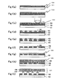
- Figures 1 (a) to 1 (i) are illustrations showing steps of the fabrication method of a stamper for an optical information recording medium of the Embodiment 1.
- an etching layer made of an acrylic material (content of 90% or more) 102 is formed on an Si substrate 101 through spin coating so that the thickness uniformly becomes approx. 60 nm over the entire surface ( Figure 1(a) ).
- a resist layer 103 made of photoresist formed by an inorganic oxide material of TeOxPd (0 ⁇ x ⁇ 2) is formed on the etching layer 102 ( Figure 1 (b) ).
- the resist layer 103 is removed by an exfoliating solution of strong acid or alkali ( Figure 1 (f) ). Thereby, a concave signal pattern 109 is formed on the resist layer 103.
- the resist layer 103 having the concave signal pattern 109 and the Si substrate 101 constitute a master disk of a stamper.
- a conductive film 105 is formed on the surface of the etching layer 102 on which the concave signal pattern 109 is formed through dry etching in accordance with metal sputtering of Ni or the like ( Figure 1 (g) ).
- electroforming is performed by using the conductive film 105 as an electrode to form a metallic layer 106 having a thickness of hundreds of microns ( Figure 1 (h) ).
- the portion constituted by the conductive film 105 andmetallic layer 106 is exfoliated from the etching layer 102 and Si substrate 101.
- a stamper 107 constituted by the conductive film 105 and metallic layer 106 is obtained.
- the concave signal pattern 109 shown in Figure 1(f) is formed by the etching used for the concave pattern 108 formed on the resist layer 103 which is photoresist in the etching layer 102.
- the etching layer 102 it is not necessary to use a layer having a photoresist-like crystal structure like a conventional example as the etching layer 102 but it is possible to use a material not causing an electrical reaction such as an oxidation-reduction reaction due to application of a voltage during electroforming.
- an electrical reaction such as an oxidation-reduction reaction does not occur in the etching layer 102 by applying a voltage during electroforming or the conductive film 105 is not influenced.
- an electrical reaction such as an oxidation-reduction reaction does not occur in the etching layer 102 by applying a voltage during electroforming or the conductive film 105 is not influenced.
- the resist layer 103 is an example of photoresist of the present invention and an acrylic material forming the etching layer 102 is an example of materials having an acid resistance of the present invention.
- TeOxPd forming the resist layer 103 is an example of inorganic oxide different from a material having an acid resistance of the present invention in material quality or composition.
- the exposed portion 104 is an example of a specific portion of a resist layer of the present invention.
- the configuration shown in Figure 1(e) after dry-etching the portion of the etching layer 102 is an example of the master disk of a stamper for an optical information recording medium of the present invention.
- any method can be used to form an acrylic material as long as a uniform film thickness can be obtained by the method and a method is not restricted to the above spin coating method.
- a material mainly containing acrylic is used.
- the same preferable characteristic can be obtained also by using a material (content of 90% or more) such as polyimide, which has a resistance against an alkali developer and acid developer and forms other organic film which can be etched by oxygen gas.
- the resist layer 103 made of inorganic oxide formed on the etching layer 102 is normally formed through sputtering or vapor deposition method in vacuum as shown in Figure 1 (b) .
- this Embodiment 1 uses the TeOxPd (0 ⁇ x ⁇ 2) material as an inorganic oxide material, it is possible to use semimetal such as Te, Ge, Sb, Sn, Bi, or Se, semimetal compound, and oxide or nitride of the compound.
- materials capable of withstanding dry etching using oxygen gas as a mask such as transition metals including Ti, Nb, Ta, Mo, W, and Pd, transition metal compound, and oxide or nitride of the compound.
- a semiconductor laser beam having a wavelength of approx. 400 nm and a condensing lens having a numerical aperture (NA) of 0.95 are used to record data in the resist layer 103 as shown in Figure 1 (c) .
- NA numerical aperture
- this Embodiment 1 uses TMAH which is an alkali developer as a developer and performs development in accordance with the spin coating method as shown in Figure 1 (d) . After the development using the alkali developer, rinsing is preformed by deionized water and drying is performed by a high-speed rotation.
- An alkali developer is not restricted to TMAH but any developer can be used as long as the developer can selectively etch the exposed portion 104. Moreover, it is allowed to use an acid developer capable of selectively etching the exposed portion 104 without being restricted to the alkali developer.
- oxygen gas is used as the etching gas of the etching layer 102 formed by an acrylic material as shown in Figure 1 (e) .
- this Embodiment 1 uses the Si substrate 101 as an etching stopper layer.
- any material can be used as long as it has an etching resistance against the gas.
- electroforming is performed by using a sulfamic-acid Ni bath having a pH of approx. 4.0, using an Ni conductive film 105 as a cathode and an Ni material to be laminated on the conductive film 105 as an anode so that the thickness of the metallic layer 106 becomes approx. 300 ⁇ m as shown in Figure 1 (h) .
- the adhesiveness between the resin material and a metallic film of Ni is improved because the collision energy of the metallic material to the resin material is large.
- electroless plating instead of sputtering
- an Ni thin film is formed on the surface of the resin material serving as the etching layer 102 only by a reduction reaction. Therefore, it is possible to decrease the adhesiveness compared to the case of sputtering.
- the collision energy is not large as the case of sputtering, it is possible to avoid surfaces of the etching layer 102 and conductive film 105 from roughening.
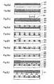
- FIG. 2 shows steps of a fabrication method of a stamper for an optical information recording medium when forming an Ni conductive film into two layers. Because steps of (a) to (f) in Figure 2 of referring to an Si substrate 201, etching layer 202, resist layer 203, exposed portion 204, concave pattern 208, and signal pattern 209 correspond to steps of (a) to (f) in Figure 1 , detailed description is omitted.
- the concave pattern 208 in Figure 2 (f) is formed so that the diameter is larger than the example shown in Figure 1(f) in order to form a conductive film into two layers.
- a first Ni thin film 205 is formed on a master disk having the Si substrate 201 and etching layer 202 through Ni sputtering to treat the surface of the first Ni thin film 205 through plasma of O 2 or Ar gas ( Figure 2 (g) ).
- a second Ni thin film 208 is formed through Ni sputtering.
- electroforming is performed by using the second Ni thin film 208 as an electrode to form a metallic layer 206 having a thickness of hundreds of microns ( Figure 2 (i) ) , a portion constituted by the second Ni thin film 208 and metallic layer 206 is exfoliated from the first Ni thin film 205 to obtain a stamper 207 ( Figure 2 (j) ).
- exfoliation layer such as an oxide film on the surface of the first Ni thin film 205 through plasma treatment of O 2 or Ar gas, exfoliation can be easily made by the first Ni thin film 205 and the second Ni thin film 208.
- Figure 3 shows a relation between thicknesses of the etching layer 102 and signal characteristics of an optical information disk fabricated from the stamper 107 fabricated by the fabrication method of a stamper for an optical information recording medium of this Embodiment 1 in the method.
- the optical information disk is like a disk allowing high-density recording, for example, a Blu-ray disk corresponding disk and corresponds to a high-density optical information recording medium of the present invention.
- the stamper 107 is fabricated in accordance with the fabrication method of a stamper for an optical information recordingmedium of this Embodiment 1.
- a signal face formed on the stamper 107 is transferred to a polycarbonate resin in accordance with the injection compression molding of polycarbonate by using the stamper 107 as a mold.
- a reflection film and a transparent cover layer are formed on the transferred signal face of the polycarbonate to fabricate a disk.
- Figure 3 shows a result of measuring the signal characteristic of the fabricated disk.
- a signal used for this Embodiment 1 uses a 1-7 modulation format and has a track pitch of 0.32 ⁇ m and minimum pit length of 0.149 ⁇ m.
- a pit width that is, the dimension at the side orthogonal to the read direction is 0.15 ⁇ m.
- the fabricated optical information disk is a disk having a diameter of 12 cm, which can accumulate the information having a capacity of 25 GB.
- a reflection mainly containing Ag is formed on the signal face of an injection-compression-molded substrate having a thickness of t1.1 mm up to approx. 50 nm and a transparent cover layer having a thickness of t0.1 mm and serving as a reproduced light projection face is formed on the reflection film.
- a reproducing head used to reproduce the fabricated disk the wavelength of a laser beam is approx. 400 nm and the numerical aperture (NA) of a condensing lens of narrowing down the laser beam is 0.85.
- NA numerical aperture
- a signal jitter measuring method is used as a method of measuring a signal characteristic.
- the signal jitter measuring method is a method in which a jitter value increases when the fluctuation of a shape such as a size or depth of a formed individual signal is large.
- a jitter value serving as an index of a disk having a preferable reproducing characteristic is generally set to 6.5% or less.
- a jitter value of 6.5% or less is satisfied as a signal characteristics of a disk when the thickness of the etching layer 102 ranges between 40 and 10 nm. When the thickness of the etching layer 102 is 40 nm or less, the depth of a signal is too shallower than the depth of approx.
- the S/N of a reproduced signal is not sufficient.
- the thickness of the etching layer 102 is 110 nm or more, it is too thicker than the depth of approx. 70 nm at which the S/N of the reproduced signal is most preferably obtained and it is considered that imperfect transfer occurs because a signal depth is too large in the injection compression step of polycarbonate.
- an optical information disk having a preferable signal characteristic can be fabricated from the stamper 107 fabricated by setting the thickness of the etching layer 102 in a range between 40 and 100 nm (both included).
- Figure 7 shows a relation between selection ratios of etching rates of the etching layer 102 and etching rates of the resist layer 103 (etching rates of the etching layer 102/etching rates of the resist layer 103) and signal characteristics of an optical information disk fabricated from the fabricated stamper 107 according to the fabrication method of a stamper for an optical information recording medium of the Embodiment 1.
- a selection ratio between the etching rate of the etching layer 102 and the etching rate of the resist layer 103 gives a ratio between the depth and the pit width of the concave pattern 108 formed in a master disk (aspect ratio) respectively corresponding to the depth and the pit width of a signal pit of the optical information disk is provided.
- the depth and diameter of the concave pattern 108 provide the height and the diameter of a convex portion serving as a transfer pattern of the stamper.
- the selection ratio also influences the accuracy of the fabricated optical information disk.
- the stamper 107 is fabricated in accordance with the fabrication method of a stamper for an optical information recording medium of this Embodiment 1.
- the stamper 107 as a mold, the signal face formed on the stamper 107 is transferred to polycarbonate resin in accordance with polycarbonate injection compression molding. Then, a reflection film and a transparent layer are formed on the transferred signal face of the polycarbonate to fabricate a disk.
- Figure 7 shows a result of measuring the signal characteristic of the fabricated disk. Other conditions are basically the same as those of the example shown in Figure 3 .
- a jitter value of 6.5% or less is satisfied at a selection ratio of approx. 0. 88 as the signal characteristic of a disk. Moreover, when exceeding 1, the jitter value reaches approx. 5.5% and thereafter, substantially becomes constant even if increasing the selection ratio.
- the selection ratio is 1 or less, the diameter of a concave portion corresponding to a signal pit becomes larger than the depth of the concave portion and it is considered that the S/N of a reproduced signal is not sufficient. Moreover, when the selection ratio exceeds 1, it is considered that the S/N of the reproduced signal reaches a limit, since the absolute values of the size or the depth of the pit no longer vary.
- an optical information disk having a preferable signal characteristic can be fabricated from the stamper 107 fabricated by substantially setting the selection ratio between the etching rate of the etching layer 102 and the etching rate of the resist layer 103 to at least 1 or more.
- a stamper for an optical information recording medium in which the ratio between the height and the diameter of a convex portion corresponding to the shape of a signal pit introduced from the selection ratio is substantially 1.0 or more is also included in the present invention.
- preferable electroforming can be made because of using a resin material withstanding an acid solution . having a pH value of 3.0 or more generally used for electroforming as the etching layer 102 and forming a concave convex pattern of signal pits on the etching layer 102. Moreover, an electrical reaction such as oxidation-reduction reaction is not caused due to application of a voltage during electroforming and therefore, the preferable stamper 107 can be fabricated. Furthermore, it is possible to fabricate a disk having a preferable signal characteristic by injection-compression-molding a substrate using the stamper 107.
- Figures 4 (a) to 4 (i) are illustrations showing steps of the fabrication method of a stamper for an optical information recording medium of the Embodiment 2 of the present invention.
- Figure 4 is different from Figure 1 which shows the Embodiment 1 in material forming an etching layer.
- the etching layer 102 is formed by an acrylic material in Figure 1
- an etching layer 302 in Figure 4 is formed by SiO 2 (content of 90% or more).
- Other configuration in Figure 4 is the same as that in Figure 1 .
- the etching layer 302 of SiO 2 is formed on an Si substrate 301 so that the thickness becomes almost uniform on the entire surface at approx. 60 nm ( Figure 4(a) ).
- a resist layer 303 which is photoresist formed by an inorganic oxide material of TeOxPd (0 ⁇ x ⁇ 2) is formed on the etching layer 302 ( Figure 4 (b) ).
- the exposed portion 304 whose crystal states are changed is selectively etched by using an etching rate difference due to the difference between crystal states of the resist layer 303 and applying a developer to form a substantially mortar-shaped concave pattern 308 by the resist layer 303 ( Figure 4 (d) ).
- the resist layer 303 is removed by a strong-alkali or -acid exfoliation solution ( Figure 4 (f) ). Thereby, a concave signal pattern 309 is formed on the resist layer 303.
- the resist layer 303 having the concave signal pattern 309 and the Si substrate 301 comprises the master disk of a stamper.
- a conductive film 305 is formed on the surface of the etching layer 302 on which a concave signal pattern 109 is formed through dry etching through metallic sputtering of Ni or the like ( Figure 4 (g) ).
- a metallic layer 306 having a thickness of hundreds of microns is formed by using the conductive film 305 as an electrode and thereby performing electroforming ( Figure 4 (h) ).
- the concave signal pattern 309 shown in Figure 4 (f) is formed through the etching used for the concave pattern 308 formed on the resist layer 303 which is photoresist in the etching layer 302.
- the etching layer 302 it is not necessary to use a layer having a photoresist-like crystal structure like a conventional example as the etching layer 302 but it is possible to use a material not causing an electrical reaction such as an oxidation-reduction reaction due to application of a voltage during electroforming. Therefore,an electrical reaction such as an oxidation-reduction reaction does not occur in the etching layer 102 due to application of a voltage during electroforming when fabricating a stamper. Therefore, it is possible to fabricate the preferable stamper 307.
- SiO 2 for forming the etching layer 302 is an example of materials having an acid resistance of the present invention.
- TeOxPd for forming the resist layer 303 is an example of inorganic oxides different from a material having an acid resistance of the present invention in material quality or composition.
- the exposed portion 304 is an example of a specific portion of a resist layer of the present invention.
- the configuration shown in Figure 4 (e) after dry-etching the portion of the etching layer 302 is an example of the master disk of a stamper for an optical information recording medium of the present invention.
- an SiO 2 layer is formed by any method of surface oxidation of the Si substrate 301 and deposition by sputtering or vapor evaporation.
- SiO 2 as an etching material.
- the etching material is not restricted to SiO 2 . It is allowed to use another inorganic oxide material as long as the material has a reaction property and an etching property to an etching gas, and withstands an acid solution having a pH of 3.0 or more.
- the etching gas is not restricted to CHF 3 gas.
- Mixed gas containing fluorine or other gas can be used as long as the gas has a preferable selection ratio to the resist layer 302.
- this Embodiment 2 uses the Si substrate 301 as an etching stopper layer.
- gas capable of etching an SiO 2 material it is also possible to fabricate a master disk having a preferable depth of a signal pit by using another material other than an Si material as an etching stopper layer as long as the material has an etching resistance against the gas.
- this Embodiment 2 says that one layer of the conductive film 305 is formed. However, it is also allowed to form two layers of conductive films similarly to that shown in Figure 2 for the Embodiment 1 and exfoliate a stamper between the conductive films. In this case, the same advantage as the Embodiment 1 is obtained.
- preferable electroforming can be made because of using a resin material capable of withstanding an acid solution having a pH of 3.0 or more generally used for electroforming as the etching layer 302 and forming the concave convex pattern of a signal on the etching layer 302. Moreover, it is possible to fabricate the preferable stamper 307 because an electrical reaction such as an oxidation-reduction reaction is not caused due to application of a voltage during electroforming. Furthermore, it is possible to fabricate a disk having a preferable signal characteristic by injection-compression-molding a substrate using the stamper 307. Furthermore, by using an inorganic oxide material for the etching layer 302, it is possible to preferably exfoliate the stamper 107 from a metallic material.
- the portion of a resist layer which is exposed by a laser beam and whose crystal states are changed is removed through etching to form a concave portion.
- it is also allowed to remove an unexposed portion through etching and leave a portion whose crystal states are changed to form a convex portion by a resist layer. Also in this case, the advantage same as that described for each embodiment is obtained.
- each embodiment says that a resin material or inorganic oxide material capable of withstanding an acid solution having a pH value of 3.0 or more generally used for electroforming is used as an etching layer and an inorganic oxide material is used as a resist layer.
- the present invention is not restricted by a specific composition of the material of each layer as long as an etching layer and a resist layer can be individually and selectively etched through the etching in each step.
- the width of the signal pit is 0.15 ⁇ m. However 0.18 ⁇ m, which is commonly used in the high-density optical information recording medium can be applied.
- a fabrication method of a stamper for an optical information recording medium, a master disk of a stamper for an optical information recording medium, and an optical information recording medium of the present invention have advantages that electroforming can be preferably performed and a fine signal can be formed and are useful as a fabrication method of a stamper for an optical information recording medium, master disk of a stamper for an optical information recording medium, optical information recording stamper, and optical information recording medium of fabricating a high-density optical information recording medium through the dry etching method.
Landscapes
- Engineering & Computer Science (AREA)
- Manufacturing & Machinery (AREA)
- Manufacturing Optical Record Carriers (AREA)
- Shaping Of Tube Ends By Bending Or Straightening (AREA)
Applications Claiming Priority (2)
| Application Number | Priority Date | Filing Date | Title |
|---|---|---|---|
| JP2003308416 | 2003-09-01 | ||
| JP2003308416 | 2003-09-01 |
Publications (3)
| Publication Number | Publication Date |
|---|---|
| EP1511027A2 EP1511027A2 (en) | 2005-03-02 |
| EP1511027A3 EP1511027A3 (en) | 2007-03-21 |
| EP1511027B1 true EP1511027B1 (en) | 2009-07-01 |
Family
ID=34101276
Family Applications (1)
| Application Number | Title | Priority Date | Filing Date |
|---|---|---|---|
| EP04020654A Expired - Lifetime EP1511027B1 (en) | 2003-09-01 | 2004-08-31 | Fabrication method of stamper for optical information recording medium, master disk of stamper for optical information recording medium |
Country Status (7)
| Country | Link |
|---|---|
| US (1) | US20050063289A1 (zh) |
| EP (1) | EP1511027B1 (zh) |
| KR (1) | KR20050024195A (zh) |
| CN (1) | CN100390886C (zh) |
| AT (1) | ATE435487T1 (zh) |
| DE (1) | DE602004021755D1 (zh) |
| TW (1) | TWI306600B (zh) |
Families Citing this family (9)
| Publication number | Priority date | Publication date | Assignee | Title |
|---|---|---|---|---|
| JP2007533064A (ja) | 2004-04-15 | 2007-11-15 | コーニンクレッカ フィリップス エレクトロニクス エヌ ヴィ | マスク層を有する光学マスター基板及び高密度レリーフ構造の製造方法 |
| EP1732071A1 (en) * | 2005-06-09 | 2006-12-13 | Sony Corporation | Lens positioning method, cutting method, positioning method and cutting apparatus |
| FR2909797B1 (fr) * | 2006-12-08 | 2009-02-13 | Commissariat Energie Atomique | Formation de zones en creux profondes et son utilisation lors de la fabrication d'un support d'enregistrement optique |
| JP2008269720A (ja) * | 2007-04-23 | 2008-11-06 | Canon Inc | 透光性スタンパ、透光性スタンパの製造方法及び多層光記録媒体の製造方法 |
| KR101363681B1 (ko) * | 2008-10-14 | 2014-02-14 | 아사히 가세이 이-매터리얼즈 가부시키가이샤 | 열반응형 레지스트 재료, 이를 이용한 열리소그래피용 적층체, 이들을 이용한 몰드의 제조방법 및 몰드 |
| JP4768848B2 (ja) * | 2009-12-07 | 2011-09-07 | 株式会社東芝 | 電鋳用原盤及びその製造方法 |
| KR101065707B1 (ko) * | 2010-09-16 | 2011-09-19 | 엘지전자 주식회사 | 사출금형용 스탬퍼 제작방법 |
| US9856319B2 (en) | 2012-12-28 | 2018-01-02 | Abbvie Inc. | Monovalent binding proteins |
| CN108249390A (zh) * | 2018-01-17 | 2018-07-06 | 高世雄 | 一种在聚酰亚胺薄膜表面制作微纳结构的方法 |
Family Cites Families (15)
| Publication number | Priority date | Publication date | Assignee | Title |
|---|---|---|---|---|
| US4724043A (en) * | 1984-09-04 | 1988-02-09 | International Business Machines Corporation | Process for forming a master mold for optical storage disks |
| JPS6168296A (ja) * | 1984-09-13 | 1986-04-08 | Matsushita Electric Ind Co Ltd | 光学情報記緑部材 |
| US5051340A (en) * | 1989-06-23 | 1991-09-24 | Eastman Kodak Company | Master for optical element replication |
| US5043251A (en) * | 1989-11-29 | 1991-08-27 | The United States Of America As Represented By The Secretary Of The Navy | Process of three dimensional lithography in amorphous polymers |
| FR2716563B1 (fr) * | 1994-02-21 | 1996-06-07 | Digipress Sa | Substrat préformaté, substrat préformaté comportant des informations à dupliquer, leurs procédés de fabrication et procédé de fabrication d'un disque maître et/ou d'un disque optique. |
| JP3058062B2 (ja) * | 1995-10-13 | 2000-07-04 | 日本電気株式会社 | 光ディスク用記録原盤の製造方 |
| TW525159B (en) * | 1998-05-14 | 2003-03-21 | Matsushita Electric Ind Co Ltd | Formation method for metallic stamper and metallic stamper and, manufacture method for optical disk substrate with the use of the stamper and optical disk fabricated by the manufacture method |
| EP1102248A4 (en) * | 1998-07-28 | 2004-10-20 | Matsushita Electric Ind Co Ltd | OPTICAL DISC AND OPTICAL DISC DRIVE |
| US6872511B2 (en) * | 2001-02-16 | 2005-03-29 | Sharp Kabushiki Kaisha | Method for forming micropatterns |
| JP4610770B2 (ja) * | 2001-03-30 | 2011-01-12 | キヤノン株式会社 | 光ディスク原盤の製造方法 |
| TWI292910B (zh) * | 2001-06-11 | 2008-01-21 | Sony Corp | |
| JP3592285B2 (ja) * | 2001-06-28 | 2004-11-24 | 住友電気工業株式会社 | ポリイミド層を含む積層体のエッチング方法 |
| US20030064293A1 (en) * | 2001-09-07 | 2003-04-03 | Polight Technologies Ltd. | Holographic recording medium |
| US7887711B2 (en) * | 2002-06-13 | 2011-02-15 | International Business Machines Corporation | Method for etching chemically inert metal oxides |
| EP1482494A3 (en) * | 2003-05-28 | 2007-08-29 | Matsushita Electric Industrial Co., Ltd. | Method for producing master for optical information recording media |
-
2004
- 2004-08-31 KR KR1020040068964A patent/KR20050024195A/ko not_active Application Discontinuation
- 2004-08-31 EP EP04020654A patent/EP1511027B1/en not_active Expired - Lifetime
- 2004-08-31 AT AT04020654T patent/ATE435487T1/de not_active IP Right Cessation
- 2004-08-31 TW TW093126209A patent/TWI306600B/zh not_active IP Right Cessation
- 2004-08-31 US US10/930,600 patent/US20050063289A1/en not_active Abandoned
- 2004-08-31 CN CNB2004100683404A patent/CN100390886C/zh not_active Expired - Fee Related
- 2004-08-31 DE DE602004021755T patent/DE602004021755D1/de not_active Expired - Lifetime
Also Published As
| Publication number | Publication date |
|---|---|
| DE602004021755D1 (de) | 2009-08-13 |
| EP1511027A2 (en) | 2005-03-02 |
| US20050063289A1 (en) | 2005-03-24 |
| EP1511027A3 (en) | 2007-03-21 |
| CN1591633A (zh) | 2005-03-09 |
| CN100390886C (zh) | 2008-05-28 |
| TW200518087A (en) | 2005-06-01 |
| KR20050024195A (ko) | 2005-03-10 |
| TWI306600B (en) | 2009-02-21 |
| ATE435487T1 (de) | 2009-07-15 |
Similar Documents
| Publication | Publication Date | Title |
|---|---|---|
| US6874262B2 (en) | Method for manufacturing master substrate used for manufacturing grooved molding substrate, method for manufacturing stamper for manufacturing grooved molding substrate, method for manufacturing grooved molding substrate, grooved molding substrate, memory medium, memory device, and computer | |
| KR100926858B1 (ko) | 광디스크용 원반의 제조 방법 및 광디스크의 제조 방법 | |
| US20050167867A1 (en) | Method and apparatus for making a stamper for patterning CDs and DVDs | |
| EP1511027B1 (en) | Fabrication method of stamper for optical information recording medium, master disk of stamper for optical information recording medium | |
| US20040241589A1 (en) | Method for producing master for optical information recording medium | |
| JP2005011489A (ja) | 光情報記録媒体の原盤製造方法 | |
| EP1460625A1 (en) | Information medium master manufacturing method, information medium stamper manufacturing method, information medium master manufacturing apparatus, and information medium stamper manufacturing apparatus | |
| JP2002298449A (ja) | 光ディスク原盤、光ディスク基板用スタンパー、及びこれらの製造方法、並びに光磁気記録媒体 | |
| US6127100A (en) | Method of manufacturing a stamper for use in optical information recording medium | |
| US7955786B2 (en) | Production of a multilayer optical recording medium using a stamper | |
| US20060290018A1 (en) | Process for produicng stamper for direct mastering, and stamper produced by such process and optical disc | |
| JP2005100608A (ja) | 光情報記録媒体用スタンパの製造方法、光情報記録媒体用スタンパ、光情報記録媒体用スタンパの原盤および光情報記録媒体 | |
| JPH09115190A (ja) | 光ディスク用スタンパの製造方法 | |
| JP2008287762A (ja) | 透光性スタンパ及びその原盤 | |
| JP4093938B2 (ja) | 光情報記録媒体の原盤製造方法、パターン形成方法およびレジスト | |
| JP2008226287A (ja) | 光ディスク用スタンパ及びその製造方法 | |
| EP1609614B1 (en) | Optical recording medium | |
| US20030193101A1 (en) | Super resolution optical disk mother mold | |
| JP3230313B2 (ja) | 反応性イオンエッチングによるパターニング加工物の製造方法 | |
| JP2007265593A (ja) | 光ディスク、光ディスク基板および光ディスク原盤ならびに、これらの製造方法 | |
| JP2739841B2 (ja) | 情報記録媒体の製造方法 | |
| JP2001243662A (ja) | 記録媒体の製造方法、および記録媒体製造用原盤の製造方法 | |
| JP2000242984A (ja) | 光記録媒体およびその製造方法 | |
| JP2006004587A (ja) | ピットパターンの形成方法,読取専用光ディスク原盤,読取専用光ディスクスタンパの製造方法,読取専用光ディスクスタンパおよび読取専用光ディスク基板 | |
| JP2000021017A (ja) | 光学記録媒体と光学記録媒体の製造方法、および光学記録媒体用基板と光学記録媒体用基板の製造方法 |
Legal Events
| Date | Code | Title | Description |
|---|---|---|---|
| PUAI | Public reference made under article 153(3) epc to a published international application that has entered the european phase |
Free format text: ORIGINAL CODE: 0009012 |
|
| AK | Designated contracting states |
Kind code of ref document: A2 Designated state(s): AT BE BG CH CY CZ DE DK EE ES FI FR GB GR HU IE IT LI LU MC NL PL PT RO SE SI SK TR |
|
| AX | Request for extension of the european patent |
Extension state: AL HR LT LV MK |
|
| PUAL | Search report despatched |
Free format text: ORIGINAL CODE: 0009013 |
|
| AK | Designated contracting states |
Kind code of ref document: A3 Designated state(s): AT BE BG CH CY CZ DE DK EE ES FI FR GB GR HU IE IT LI LU MC NL PL PT RO SE SI SK TR |
|
| AX | Request for extension of the european patent |
Extension state: AL HR LT LV MK |
|
| 17P | Request for examination filed |
Effective date: 20070907 |
|
| 17Q | First examination report despatched |
Effective date: 20071008 |
|
| AKX | Designation fees paid |
Designated state(s): AT BE BG CH CY CZ DE DK EE ES FI FR GB GR HU IE IT LI LU MC NL PL PT RO SE SI SK TR |
|
| RAP1 | Party data changed (applicant data changed or rights of an application transferred) |
Owner name: PANASONIC CORPORATION |
|
| GRAP | Despatch of communication of intention to grant a patent |
Free format text: ORIGINAL CODE: EPIDOSNIGR1 |
|
| RTI1 | Title (correction) |
Free format text: FABRICATION METHOD OF STAMPER FOR OPTICAL INFORMATION RECORDING MEDIUM, MASTER DISK OF STAMPER FOR OPTICAL INFORMATION RECORDING MEDIUM |
|
| GRAS | Grant fee paid |
Free format text: ORIGINAL CODE: EPIDOSNIGR3 |
|
| GRAA | (expected) grant |
Free format text: ORIGINAL CODE: 0009210 |
|
| AK | Designated contracting states |
Kind code of ref document: B1 Designated state(s): AT BE BG CH CY CZ DE DK EE ES FI FR GB GR HU IE IT LI LU MC NL PL PT RO SE SI SK TR |
|
| REG | Reference to a national code |
Ref country code: GB Ref legal event code: FG4D |
|
| REG | Reference to a national code |
Ref country code: CH Ref legal event code: EP |
|
| REG | Reference to a national code |
Ref country code: IE Ref legal event code: FG4D |
|
| REF | Corresponds to: |
Ref document number: 602004021755 Country of ref document: DE Date of ref document: 20090813 Kind code of ref document: P |
|
| PG25 | Lapsed in a contracting state [announced via postgrant information from national office to epo] |
Ref country code: SI Free format text: LAPSE BECAUSE OF FAILURE TO SUBMIT A TRANSLATION OF THE DESCRIPTION OR TO PAY THE FEE WITHIN THE PRESCRIBED TIME-LIMIT Effective date: 20090701 |
|
| NLV1 | Nl: lapsed or annulled due to failure to fulfill the requirements of art. 29p and 29m of the patents act | ||
| PG25 | Lapsed in a contracting state [announced via postgrant information from national office to epo] |
Ref country code: AT Free format text: LAPSE BECAUSE OF FAILURE TO SUBMIT A TRANSLATION OF THE DESCRIPTION OR TO PAY THE FEE WITHIN THE PRESCRIBED TIME-LIMIT Effective date: 20090701 Ref country code: EE Free format text: LAPSE BECAUSE OF FAILURE TO SUBMIT A TRANSLATION OF THE DESCRIPTION OR TO PAY THE FEE WITHIN THE PRESCRIBED TIME-LIMIT Effective date: 20090701 Ref country code: FI Free format text: LAPSE BECAUSE OF FAILURE TO SUBMIT A TRANSLATION OF THE DESCRIPTION OR TO PAY THE FEE WITHIN THE PRESCRIBED TIME-LIMIT Effective date: 20090701 Ref country code: ES Free format text: LAPSE BECAUSE OF FAILURE TO SUBMIT A TRANSLATION OF THE DESCRIPTION OR TO PAY THE FEE WITHIN THE PRESCRIBED TIME-LIMIT Effective date: 20091012 Ref country code: SE Free format text: LAPSE BECAUSE OF FAILURE TO SUBMIT A TRANSLATION OF THE DESCRIPTION OR TO PAY THE FEE WITHIN THE PRESCRIBED TIME-LIMIT Effective date: 20090701 |
|
| PG25 | Lapsed in a contracting state [announced via postgrant information from national office to epo] |
Ref country code: NL Free format text: LAPSE BECAUSE OF FAILURE TO SUBMIT A TRANSLATION OF THE DESCRIPTION OR TO PAY THE FEE WITHIN THE PRESCRIBED TIME-LIMIT Effective date: 20090701 Ref country code: PL Free format text: LAPSE BECAUSE OF FAILURE TO SUBMIT A TRANSLATION OF THE DESCRIPTION OR TO PAY THE FEE WITHIN THE PRESCRIBED TIME-LIMIT Effective date: 20090701 |
|
| PG25 | Lapsed in a contracting state [announced via postgrant information from national office to epo] |
Ref country code: PT Free format text: LAPSE BECAUSE OF FAILURE TO SUBMIT A TRANSLATION OF THE DESCRIPTION OR TO PAY THE FEE WITHIN THE PRESCRIBED TIME-LIMIT Effective date: 20091102 Ref country code: MC Free format text: LAPSE BECAUSE OF NON-PAYMENT OF DUE FEES Effective date: 20090831 Ref country code: BG Free format text: LAPSE BECAUSE OF FAILURE TO SUBMIT A TRANSLATION OF THE DESCRIPTION OR TO PAY THE FEE WITHIN THE PRESCRIBED TIME-LIMIT Effective date: 20091001 |
|
| REG | Reference to a national code |
Ref country code: CH Ref legal event code: PL |
|
| PG25 | Lapsed in a contracting state [announced via postgrant information from national office to epo] |
Ref country code: CZ Free format text: LAPSE BECAUSE OF FAILURE TO SUBMIT A TRANSLATION OF THE DESCRIPTION OR TO PAY THE FEE WITHIN THE PRESCRIBED TIME-LIMIT Effective date: 20090701 Ref country code: RO Free format text: LAPSE BECAUSE OF FAILURE TO SUBMIT A TRANSLATION OF THE DESCRIPTION OR TO PAY THE FEE WITHIN THE PRESCRIBED TIME-LIMIT Effective date: 20090701 Ref country code: CH Free format text: LAPSE BECAUSE OF NON-PAYMENT OF DUE FEES Effective date: 20090831 Ref country code: DK Free format text: LAPSE BECAUSE OF FAILURE TO SUBMIT A TRANSLATION OF THE DESCRIPTION OR TO PAY THE FEE WITHIN THE PRESCRIBED TIME-LIMIT Effective date: 20090701 Ref country code: LI Free format text: LAPSE BECAUSE OF NON-PAYMENT OF DUE FEES Effective date: 20090831 |
|
| PLBE | No opposition filed within time limit |
Free format text: ORIGINAL CODE: 0009261 |
|
| STAA | Information on the status of an ep patent application or granted ep patent |
Free format text: STATUS: NO OPPOSITION FILED WITHIN TIME LIMIT |
|
| PG25 | Lapsed in a contracting state [announced via postgrant information from national office to epo] |
Ref country code: SK Free format text: LAPSE BECAUSE OF FAILURE TO SUBMIT A TRANSLATION OF THE DESCRIPTION OR TO PAY THE FEE WITHIN THE PRESCRIBED TIME-LIMIT Effective date: 20090701 Ref country code: BE Free format text: LAPSE BECAUSE OF FAILURE TO SUBMIT A TRANSLATION OF THE DESCRIPTION OR TO PAY THE FEE WITHIN THE PRESCRIBED TIME-LIMIT Effective date: 20090701 |
|
| 26N | No opposition filed |
Effective date: 20100406 |
|
| PG25 | Lapsed in a contracting state [announced via postgrant information from national office to epo] |
Ref country code: IE Free format text: LAPSE BECAUSE OF NON-PAYMENT OF DUE FEES Effective date: 20090831 |
|
| PG25 | Lapsed in a contracting state [announced via postgrant information from national office to epo] |
Ref country code: GR Free format text: LAPSE BECAUSE OF FAILURE TO SUBMIT A TRANSLATION OF THE DESCRIPTION OR TO PAY THE FEE WITHIN THE PRESCRIBED TIME-LIMIT Effective date: 20091002 |
|
| PG25 | Lapsed in a contracting state [announced via postgrant information from national office to epo] |
Ref country code: IT Free format text: LAPSE BECAUSE OF FAILURE TO SUBMIT A TRANSLATION OF THE DESCRIPTION OR TO PAY THE FEE WITHIN THE PRESCRIBED TIME-LIMIT Effective date: 20090701 |
|
| PG25 | Lapsed in a contracting state [announced via postgrant information from national office to epo] |
Ref country code: LU Free format text: LAPSE BECAUSE OF NON-PAYMENT OF DUE FEES Effective date: 20090831 |
|
| PG25 | Lapsed in a contracting state [announced via postgrant information from national office to epo] |
Ref country code: HU Free format text: LAPSE BECAUSE OF FAILURE TO SUBMIT A TRANSLATION OF THE DESCRIPTION OR TO PAY THE FEE WITHIN THE PRESCRIBED TIME-LIMIT Effective date: 20100102 |
|
| PG25 | Lapsed in a contracting state [announced via postgrant information from national office to epo] |
Ref country code: TR Free format text: LAPSE BECAUSE OF FAILURE TO SUBMIT A TRANSLATION OF THE DESCRIPTION OR TO PAY THE FEE WITHIN THE PRESCRIBED TIME-LIMIT Effective date: 20090701 |
|
| PG25 | Lapsed in a contracting state [announced via postgrant information from national office to epo] |
Ref country code: CY Free format text: LAPSE BECAUSE OF FAILURE TO SUBMIT A TRANSLATION OF THE DESCRIPTION OR TO PAY THE FEE WITHIN THE PRESCRIBED TIME-LIMIT Effective date: 20090701 |
|
| PGFP | Annual fee paid to national office [announced via postgrant information from national office to epo] |
Ref country code: FR Payment date: 20110818 Year of fee payment: 8 Ref country code: GB Payment date: 20110831 Year of fee payment: 8 Ref country code: DE Payment date: 20110824 Year of fee payment: 8 |
|
| GBPC | Gb: european patent ceased through non-payment of renewal fee |
Effective date: 20120831 |
|
| REG | Reference to a national code |
Ref country code: FR Ref legal event code: ST Effective date: 20130430 |
|
| PG25 | Lapsed in a contracting state [announced via postgrant information from national office to epo] |
Ref country code: GB Free format text: LAPSE BECAUSE OF NON-PAYMENT OF DUE FEES Effective date: 20120831 Ref country code: DE Free format text: LAPSE BECAUSE OF NON-PAYMENT OF DUE FEES Effective date: 20130301 |
|
| PG25 | Lapsed in a contracting state [announced via postgrant information from national office to epo] |
Ref country code: FR Free format text: LAPSE BECAUSE OF NON-PAYMENT OF DUE FEES Effective date: 20120831 |
|
| REG | Reference to a national code |
Ref country code: DE Ref legal event code: R119 Ref document number: 602004021755 Country of ref document: DE Effective date: 20130301 |