EP1510000B1 - Operationsverstärker mit unabhängiger eingangsoffsettrimmung für hohe und niedrige gleichtakt-eingangsspannungen - Google Patents
Operationsverstärker mit unabhängiger eingangsoffsettrimmung für hohe und niedrige gleichtakt-eingangsspannungen Download PDFInfo
- Publication number
- EP1510000B1 EP1510000B1 EP03760203A EP03760203A EP1510000B1 EP 1510000 B1 EP1510000 B1 EP 1510000B1 EP 03760203 A EP03760203 A EP 03760203A EP 03760203 A EP03760203 A EP 03760203A EP 1510000 B1 EP1510000 B1 EP 1510000B1
- Authority
- EP
- European Patent Office
- Prior art keywords
- current
- input
- trim
- differential
- common mode
- Prior art date
- Legal status (The legal status is an assumption and is not a legal conclusion. Google has not performed a legal analysis and makes no representation as to the accuracy of the status listed.)
- Expired - Lifetime
Links
Images

Classifications
-
- H—ELECTRICITY
- H03—ELECTRONIC CIRCUITRY
- H03F—AMPLIFIERS
- H03F3/00—Amplifiers with only discharge tubes or only semiconductor devices as amplifying elements
- H03F3/45—Differential amplifiers
- H03F3/45071—Differential amplifiers with semiconductor devices only
- H03F3/45479—Differential amplifiers with semiconductor devices only characterised by the way of common mode signal rejection
- H03F3/45632—Differential amplifiers with semiconductor devices only characterised by the way of common mode signal rejection in differential amplifiers with FET transistors as the active amplifying circuit
- H03F3/45744—Differential amplifiers with semiconductor devices only characterised by the way of common mode signal rejection in differential amplifiers with FET transistors as the active amplifying circuit by offset reduction
- H03F3/45766—Differential amplifiers with semiconductor devices only characterised by the way of common mode signal rejection in differential amplifiers with FET transistors as the active amplifying circuit by offset reduction by using balancing means
-
- H—ELECTRICITY
- H03—ELECTRONIC CIRCUITRY
- H03F—AMPLIFIERS
- H03F3/00—Amplifiers with only discharge tubes or only semiconductor devices as amplifying elements
- H03F3/45—Differential amplifiers
- H03F3/45071—Differential amplifiers with semiconductor devices only
- H03F3/45076—Differential amplifiers with semiconductor devices only characterised by the way of implementation of the active amplifying circuit in the differential amplifier
- H03F3/45376—Differential amplifiers with semiconductor devices only characterised by the way of implementation of the active amplifying circuit in the differential amplifier using junction FET transistors as the active amplifying circuit
- H03F3/45408—Complementary long tailed pairs having parallel inputs and being supplied in parallel
- H03F3/45417—Folded cascode stages
-
- H—ELECTRICITY
- H03—ELECTRONIC CIRCUITRY
- H03F—AMPLIFIERS
- H03F2203/00—Indexing scheme relating to amplifiers with only discharge tubes or only semiconductor devices as amplifying elements covered by H03F3/00
- H03F2203/45—Indexing scheme relating to differential amplifiers
- H03F2203/45028—Indexing scheme relating to differential amplifiers the differential amplifier amplifying transistors are folded cascode coupled transistors
-
- H—ELECTRICITY
- H03—ELECTRONIC CIRCUITRY
- H03F—AMPLIFIERS
- H03F2203/00—Indexing scheme relating to amplifiers with only discharge tubes or only semiconductor devices as amplifying elements covered by H03F3/00
- H03F2203/45—Indexing scheme relating to differential amplifiers
- H03F2203/45048—Calibrating and standardising a dif amp
-
- H—ELECTRICITY
- H03—ELECTRONIC CIRCUITRY
- H03F—AMPLIFIERS
- H03F2203/00—Indexing scheme relating to amplifiers with only discharge tubes or only semiconductor devices as amplifying elements covered by H03F3/00
- H03F2203/45—Indexing scheme relating to differential amplifiers
- H03F2203/45308—Indexing scheme relating to differential amplifiers the common gate stage of a cascode dif amp being implemented as one mirror circuit
-
- H—ELECTRICITY
- H03—ELECTRONIC CIRCUITRY
- H03F—AMPLIFIERS
- H03F2203/00—Indexing scheme relating to amplifiers with only discharge tubes or only semiconductor devices as amplifying elements covered by H03F3/00
- H03F2203/45—Indexing scheme relating to differential amplifiers
- H03F2203/45466—Indexing scheme relating to differential amplifiers the CSC being controlled, e.g. by a signal derived from a non specified place in the dif amp circuit
Definitions
- This invention relates to the field of trim circuits, and particularly to trim circuits for operational amplifiers which employ complementary input pairs to achieve a rail-to-rail common mode input range.
- V os input offset voltage
- V os input offset voltage
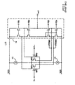
- FIG. 1 One example of an op amp with a trimmable V os is shown in FIG. 1; this approach is described in U.S. Patent No. 6,194,962 to Chen.
- the op amp's input consists of a first differential transistor pair MN1 and MN2, and a complementary differential transistor pair MP1 and MP2; both input pairs are connected to receive a differential input signal applied to input terminals V+ and V-.
- MN1 and MN2 are biased with a tail current source 10 and MP1 and MP2 receive a tail current from a source 12.
- each input pair produces a differential current that feeds in to a folded cascode stage 14, which produces an output current I out that varies with the differential currents received from the input pairs.
- a pair of trim inputs TRIM1 and TRIM2 are connected to respective nodes of the folded cascode stage 14.
- the PMOS input pair (MP1, MP2) is active when the input common mode voltage (V cm ) is low (below a pre-set threshold voltage), and the NMOS input pair is active when V cm is high (above the pre-set threshold voltage).
- V cm input common mode voltage
- NMOS input pair is active when V cm is high (above the pre-set threshold voltage).
- a first correction current ⁇ I1 is applied to TRIM1 or TRIM2 to reduce V os to zero.
- the correction provided by ⁇ I1 is given by ⁇ I1/gmp, where gmp is the transconductance of PMOS transistors MP1 and MP2; correction current ⁇ I1 is applied throughout the entire common mode input range.
- ⁇ I1 After ⁇ I1 has been set, a high V cm is applied to the op amp, and a second correction current ⁇ I2 is applied to TRIM1 or TRIM2 (with ⁇ I1 still applied) to reduce V os .
- the correction provided by ⁇ I1 and ⁇ I2 is given by ( ⁇ I1+ ⁇ I2)/gmn, where gmn is the transconductance of NMOS transistors MN1 and MN2, since ⁇ I1 is present throughout the entire common mode input range, while ⁇ I2 is only present at high V cm .
- the trim range for a high V cm offset has to be larger than the untrimmed offset range, due to the effect of the low V cm correction current ⁇ I1.
- the trim range for low V cm can the be set at ⁇ 2.5mV, but the trim range for a high V cm has to be set at ⁇ 5mV.
- any supply voltage or V cm dependent mismatch of ⁇ I1 and ⁇ I2 leads to a supply/V cm dependence for the post-trim V os at high V cm .
- This approach also places a constraint on the procedure used to calibrate the op amp, requiring that the calibration be done in a prescribed sequence.
- the present op amp provides independent trimming of V os for both high and low common mode input voltages.
- the amplifier includes complementary input pairs, and employs a steering circuit which provides a tail current I tail to one input pair when V cm is less than a threshold voltage V th , and provides I tail to the other input pair when V cm is greater than V th .
- the input pairs produces an output current I out through a load stage; I out varies with the pairs' differential output currents.
- the load stage which is preferably a folded cascode stage, includes one or more trim inputs which enable V os to be varied with one or more trim signals applied to the trim inputs.
- a first trim signal generating circuit provides a first trim signal to a trim input only when V cm is less V th
- a second trim signal generating circuit provides a second trim signal to a trim input only when V cm is greater than V th . This allows the input offset voltages at high and low V cm to be adjusted independently, thereby avoiding the problems identified above.
- the steering circuit includes a steering transistor which steers tail current to a PMOS input pair when V cm is less than a threshold voltage V th , and to a NMOS input pair via a current mirror circuit when V cm > V th .
- a first trim signal generating circuit generates a first trim signal, suitable for trimming V os at low V cm (PMOS pair active), by mirroring a fixed bias current to a first digital-to-analog converter (DAC) which produces the first trim signal in response.
- a second trim signal generating circuit generates a second trim signal suitable for trimming V os at high V cm (NMOS pair active) when tail current is steered to the NMOS input pair.
- a diverting circuit is connected to divert the fixed bias current when tail current is steered to the NMOS input pair, such that the first trim signal is reduced to zero.
- the first trim signal can be tailored to trim V os at low v cm
- the second trim signal trims V os at high V cm
- each trim signal can be independently varied without affecting the other.
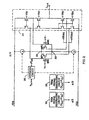
- the op amp includes complementary input pairs: an NMOS pair MN1, MN2, and a PMOS pair MP1, MP2; each is connected to receive a differential input signal at input terminals V+ and V-.
- the PMOS' sources are connected together at a common mode node 20, and the NMOS' sources are connected together at a common mode node 22.
- Each input pair produces a differential current that is fed to a load stage 18 - preferably implemented as a folded cascode stage - which produces an output current I out that varies with the input voltage applied to the input pairs.
- Load stage 18 includes at least one trim input (two trim inputs, TRIM1 and TRIM2, are shown in the exemplary embodiment shown in FIG. 2), and is arranged such that the op amp's input offset voltage V os can be varied by applying one or more trim signals to the trim inputs.
- the op amp includes a steering circuit 24, which is arranged to provide tail current to one or the other of the input pairs depending on the relationship between the differential input signal's common mode input voltage V cm and a threshold voltage V th .
- Steering circuit 24 provides a tail current I tail to common mode node 20 when V cm is less than V th , and provides I tail to common mode node 22 when V cm is greater than V th .
- the op amp also includes a first trim signal generating circuit 26 and a second trim signal generating circuit 28.
- Circuit 26 is arranged to provide a first trim signal ⁇ I1 to at least one of the op amp's trim inputs only when V cm is less than V th .
- circuit 28 is arranged to provide a second trim signal ⁇ I2 to at least one of the op amp's trim inputs only when V cm is greater than V th .
- the trim signal generating circuits are arranged such that first trim signal ⁇ I1 is set to trim V os for a low V cm , and second trim signal ⁇ I2 is set to trim V os for a high V cm .
- the present op amp is arranged such that trim signals ⁇ I1 and ⁇ I2 can be independently varied without affecting the other. This provides several advantages over the prior art approach described above.
- the trim range for a high V cm offset is no longer required to be widened because of the adverse effect of the low V cm trim signal - the trim ranges can be set solely by the untrimmed offset voltage range for both high and low common mode input voltages.
- the independent trim signal generating circuits eliminate problems caused by supply voltage or V cm dependent mismatch of ⁇ I1 and ⁇ I2, and remove constraints that were previously imposed on the amplifier's calibration procedure.
- steering circuit 24 is made from a fixed current source 30 which outputs tail current I tail , a steering transistor MP3, and a current mirror made from an input transistor MN3 and an output transistor MN4.
- Steering transistor MP3 has its source-drain circuit connected between common mode node 20 and current mirror input transistor MN3, and its gate connected to a bias voltage V th .
- V cm ⁇ V th steering transistor MP3 is off and I tail is provided to common mode node 20 and the PMOS input pair.
- V cm > V th steering transistor MP3 is on and conducts I tail to the current mirror, which mirrors the tail current to common mode node 22 and the NMOS input pair.
- Trim signal generating circuit 26 is preferably made from a fixed current source 32 which outputs a bias current 11, a current mirror made from an input transistor MN5 and an output transistor MN6, and a DAC 34.
- the MN5/MN6 current mirror mirrors I1 to the reference current input of DAC 34.
- DAC 34 produces correction current ⁇ I1, which is connected to one of the trim inputs of load stage 18.
- Trim signal generating circuit 28 is preferably made from a transistor MN7 connected to conduct a current 12 when steering transistor MP3 steers I tail to the MN3/MN4 current mirror, and a DAC 36.
- Current I2 is applied to the reference current input of DAC 36, which produces correction current ⁇ I2 in response; ⁇ I2 is connected to one of the trim inputs of load stage 18. Since 12 is only present when steering transistor MP3 steers I tail to the MN3/MN4 current mirror (i.e., when V cm > V th ), ⁇ I2 is only generated when V cm > V th .
- the operational amplifier also includes a diverting circuit 38, which is arranged to divert bias current I1 from the MN5/MN6 current mirror when steering transistor MP3 steers I tail to the MN3/MN4 current mirror, which serves to reduce or eliminate correction current ⁇ I1.
- a diverting circuit 38 preferably comprises a diverting transistor MN8 which is connected to the output of fixed current source 32 and in parallel with MN7.
- MN8 diverts current 11 away from the MN5/MN6 current mirror when steering transistor MP3 steers I tail to the MN3/MN4 current mirror; i.e, when V cm > V th . In this way, the drive current to DAC 34 is reduced or eliminated, as is correction current ⁇ I1.
- the op amp is preferably arranged with trim input TRIM1 as a "positive" trim input, such that the application of a positive trim signal ⁇ I1 or ⁇ I2 reduces a positive V os , and with TRIM2 as a "negative" trim input which reduces a negative V os with the application of a positive trim signal ⁇ I1 or ⁇ I2.
- trim input TRIM1 as a "positive" trim input, such that the application of a positive trim signal ⁇ I1 or ⁇ I2 reduces a positive V os
- TRIM2 as a "negative” trim input which reduces a negative V os with the application of a positive trim signal ⁇ I1 or ⁇ I2.
- DACs 34 and 36 could each be designed to output positive or negative trim signals. In this case, only one trim input would be needed, to which both ⁇ I1 and ⁇ I2 would be connected.
- FIG. 3 is merely one possible way of implementing the invention. A number of mechanisms could be employed to ensure that ⁇ I1 is generated only when V cm ⁇ V th , and that ⁇ I2 is generated only when V cm > V th .
- the invention can be used with other load topologies: the implementation of load stage 18 shown in FIGs. 1-3 is merely exemplary.
- the implementation shown in FIG. 3 can be a single-stage operational amplifier, or the first stage of a multistage operational amplifier.
Landscapes
- Engineering & Computer Science (AREA)
- Power Engineering (AREA)
- Amplifiers (AREA)
Claims (10)
- Operationsverstärker mit unabhängiger Eingangsoffsettrimmung für hohe und niedrige Gleichtakteingangsspannungen, umfassend:eine Eingangsstufe, umfassend:ein erstes differentielles Transistorpaar (MP1, MP2), das verbunden ist, um ein differentielles Eingangssignal zu empfangen und einen ersten differentiellen Ausgangsstrom zu erzeugen, der sich mit dem differentiellen Eingangssignal ändert, wobei die Stromschaltungen des ersten differentiellen Paares an einem ersten Gleichtaktknoten (20) miteinander verbunden sind,ein zweites differentielles Transistorpaar (MN1, MN2), das komplementär zu dem ersten Paar ist, und das verbunden ist, um das differentielle Eingangssignal zu empfangen und einen zweiten differentiellen Ausgangsstrom zu erzeugen, der sich mit dem differentiellen Eingangssignal ändert, wobei die Stromschaltungen des zweiten differentiellen Paares an einem zweiten Gleichtaktknoten (22) miteinander verbunden sind,eine Steuerschaltung (24), die einen Schwanzstrom Itail für das erste differentielle Paar an dem ersten Gleichtaktknoten bereitstellt, wenn die Gleichtaktspannung Vcm des ersten differentiellen Eingangssignals kleiner als eine Schwellenspannung Vth ist, und um Itail für das zweite differentielle Paar an dem zweiten Gleichtaktknoten bereitzustellen, wenn Vcm größer als Vth ist,eine Laststufe (14), die eingerichtet ist, um einen Ausgangsstrom (Iout) zu erzeugen, das sich mit den ersten und zweiten differentiellen Ausgangsströmen ändert, wobei die Laststufe wenigstens einen Trimmungseingang (TRIM1, TRIM2) umfasst und des Weiteren eingerichtet ist, um die Eingangsoffsetspannung des Operationsverstärkers mit einem oder mehreren Signalen zu ändern, die an dem wenigstens einen Trimmungseingang anliegen,eine erste Trimmungssignalerzeugungsschaltung (26), die eingerichtet ist, um ein erstes Trimmungssignal (ΔI1) für den wenigstens einen Trimmungseingang nur bei Vcm < Vth bereitzustellen, undeine zweite Trimmungssignalerzeugungsschaltung (28), die eingerichtet ist, um ein zweites Trimmungssignal (ΔI2) für den wenigstens einen Trimmungseingang nur bei Vcm > Vth bereitzustellen.
- Operationsverstärker nach Anspruch 1, bei dem die Steuerschaltung umfasst:eine Stromquelle (30), die verbunden ist, um Itail für den ersten Gleichtaktknoten bereitzustellen,einen Steuertransistor (MP3), dessen Stromschaltung mit dem ersten Gleichtaktknoten verbunden ist, und dessen Steuereingang derart mit Vth verbunden ist, dass der Steuertransistor einen Strom in Reaktion auf die Schwellenspannung leitet, und einen ersten Stromspiegler (MN3, MN4), der verbunden ist, um den von dem ersten Steuertransistor geleiteten Strom zu dem zweiten Gleichtaktknoten zu spiegeln.
- Operationsverstärker nach Anspruch 2, bei dem die erste Trimmungssignalerzeugungsschaltung einen ersten Vorstrom (11) empfängt und das erste Trimmungssignal in Reaktion auf den ersten Vorstrom erzeugt, wobei der Operationsverstärker des Weiteren eine Wegleitschaltung (MN8) umfasst, die den ersten Vorstrom von der ersten Trimmungssignalerzeugungsschaltung bei Vcm > Vth derart wegleitet, dass das erste Trimmungssignal auf 0 verringert wird.
- Operationsverstärker nach Anspruch 2, bei dem die zweite Trimmungssignalerzeugungsschaltung einen zweiten Vorstrom (12) empfängt und das zweite Trimmungssignal in Reaktion auf den zweiten Vorstrom erzeugt, wobei sich der zweite Vorstrom mit dem gespiegelten Strom derart ändert, dass das zweite Trimmungssignal nur bei Vcm > Vth bereitgestellt wird.
- Operationsverstärker nach Anspruch 2, bei dem die erste Trimmungssignalerzeugungsschaltung umfasst:eine Feststromquelle (32), die einen ersten Vorstrom (I1) erzeugt,einen ersten Digital-Analog-Wandler DAC (34), der das erste Trimmungssignal in Reaktion auf einen Strom erzeugt, der für den Bezugsstromeingang hiervon bereitgestellt ist, undeinen zweiten Stromspiegler (MN5, MN6), der den ersten Vorstrom empfängt und ihn zu dem Bezugsstromeingang des DAC spiegelt,wobei die zweite Stromerzeugungsschaltung umfasst:einen zweiten Digital-Analog-Wandler DAC (36), der das zweite Trimmungssignal in Reaktion auf einen Strom (I2) erzeugt, der für den Bezugsstromeingang hiervon bereitgestellt ist, undeinen Transistor (MN7), der verbunden ist, um den von dem Steuertransistor geleiteten Strom zu dem zweiten DAC zu spiegeln,des Weiteren umfassend einen Wegleittransistor (MN8), der mit dem Ausgang der Feststromquelle verbunden und eingerichtet ist, um den von dem Steuertransistor geleiteten Strom derart zu spiegeln, dass der erste Vorstrom von dem zweiten Stromspiegler bei Vcm > Vth weggeleitet wird.
- Operationsverstärker nach Anspruch 5, bei dem der Wegleittransistor derart ausgelegt ist, dass er den gesamten ersten Vorstrom derart von dem zweiten Stromspiegler wegleitet, dass das erste Trimmungssignal bei Vcm > Vth auf 0 verringert wird.
- Operationsverstärker nach Anspruch 1, bei dem die Laststufe eine Folded-Cascode-Stufe ist.
- Operationsverstärker mit unabhängiger Eingangsoffsettrimmung für hohe und niedrige Gleichtakteingangsspannungen, umfassend:eine Eingangsstufe, umfassend:ein erstes differentielles Transistorpaar (MP1, MP2), das verbunden ist, um ein differentielles Eingangssignal zu empfangen und einen ersten differentiellen Ausgangsstrom zu erzeugen, der sich mit dem differentiellen Eingangssignal ändert, wobei die Stromschaltungen des ersten differentiellen Paares an einem ersten Gleichtaktknoten (20) miteinander verbunden sind,ein zweites differentielles Transistorpaar (MN1, MN2), das komplementär zu dem ersten Paar ist, und das verbunden ist, um das differentielle Eingangssignal zu empfangen und einen zweiten differentiellen Ausgangsstrom zu er zeugen, der sich mit dem differentiellen Eingangssignal ändert, wobei die Stromschaltungen des zweiten differentiellen Paares an einem zweiten Gleichtaktknoten (22) miteinander verbunden sind,eine Steuerschaltung (24), die einen Schwanzstrom Itail für das erste differentielle Paar an dem ersten Gleichtaktknoten bereitstellt, wenn die Gleichtaktspannung Vcm des differentiellen Eingangssignals kleiner als eine Schwellenspannung Vth ist, und um Itail für das zweite differentielle Paar an dem zweiten Gleichtaktknoten bei Vcm > Vth bereitzustellen, wobei die Steuerschaltung umfasst:eine Stromquelle (30), die verbunden ist, um Itail für den ersten Gleichtaktknoten bereitzustellen,einen Steuertransistor (MP3), dessen Stromschaltung mit dem ersten Gleichtaktknoten verbunden ist, und dessen Steuereingang derart mit Vth verbunden ist, dass der Steuertransistor einen Strom in Reaktion auf die Schwellenspannung leitet, undeinen ersten Stromspiegler (MN3, MN4), der verbunden ist, um den von dem Steuertransistor geleiteten Strom zu dem zweiten Gleichtaktknoten zu spiegeln,eine Laststufe (14), die eingerichtet ist, um einen Ausgangsstrom (Iout) zu erzeugen, der sich mit den ersten und zweiten differentiellen Ausgangsströmen ändert, wobei die Laststufe wenigstens einen Trimmungseingang (TRIM1, TRIM2) umfasst und des Weiteren eingerichtet ist, um die Eingangsoffsetspannung Vos des Operationsverstärkers mit einem oder mehreren Signalen zu ändern, die an dem wenigstens einen Trimmungseingang anliegen,wobei eine erste Stromerzeugungsschaltung (26) umfasst:eine Feststromquelle (32), die einen ersten Vorstrom (I1) erzeugt,einen ersten Digital-Analog-Wandler DAC (34), der ein erstes Trimmungssignal (ΔI1) an dem wenigstens einen Trimmungseingang in Reaktion auf einen Strom erzeugt, der für den Bezugsstromeingang hiervon bereitgestellt ist, undeinen zweiten Stromspiegler (MN5, MN6), der den ersten Vorstrom empfängt und ihn zu dem Bezugsstromeingang des DAC spiegelt,wobei eine zweite Stromerzeugungsschaltung (28) umfasst:einen zweiten Digital-Analog-Wandler DAC (36), der ein zweites Trimmungssignal (ΔI2) an dem wenigstens einen Trimmungseingang in Reaktion auf einen Strom erzeugt, der an dem Bezugsstromeingang hiervon bereitgestellt ist, undeinen Transistor (MN7), der verbunden ist, um den von dem Steuertransistor geleiteten Strom zu dem zweiten DAC zu spiegeln, undeinen Wegleittransistor (MN8), der mit dem Ausgang der Feststromquelle verbunden und eingerichtet ist, um den von dem Steuertransistor geleiteten Strom derart zu spiegeln, dass der erste Vorstrom von dem zweiten Stromspiegler bei Vcm > Vth weggeleitet wird,
wobei der Wegleittransistor derart ausgelegt ist, dass er den ersten Vorstrom von dem zweiten Stromspiegler derart wegleitet, dass das erste Trimmungssignal bei Vcm > Vth auf 0 verringert wird. - Operationsverstärker nach Anspruch 8, bei dem die Laststufe eine Folded-Cascode-Stufe ist.
- Operationsverstärker nach Anspruch 8, bei dem die Trimmungseingänge der Laststufe einem positiven Trimmungseingang und einen negativen Trimmungseingang derart umfassen, dass ein an dem positiven Trimmungseingang anliegendes positives Trimmungssignal eine positive Vos verringert, und ein an dem negativen Trimmungseingang anliegendes positives Trimmungssignal eine negative Vos verringert.
Applications Claiming Priority (5)
| Application Number | Priority Date | Filing Date | Title |
|---|---|---|---|
| US38828802P | 2002-06-12 | 2002-06-12 | |
| US388288P | 2002-06-12 | ||
| US192189 | 2002-07-08 | ||
| US10/192,189 US6696894B1 (en) | 2002-06-12 | 2002-07-08 | Operational amplifier with independent input offset trim for high and low common mode input voltages |
| PCT/US2003/011919 WO2003107530A1 (en) | 2002-06-01 | 2003-04-16 | Operational amplifier with independent input offset trim for high and low common mode input voltages |
Publications (2)
| Publication Number | Publication Date |
|---|---|
| EP1510000A1 EP1510000A1 (de) | 2005-03-02 |
| EP1510000B1 true EP1510000B1 (de) | 2006-01-25 |
Family
ID=29739034
Family Applications (1)
| Application Number | Title | Priority Date | Filing Date |
|---|---|---|---|
| EP03760203A Expired - Lifetime EP1510000B1 (de) | 2002-06-12 | 2003-04-16 | Operationsverstärker mit unabhängiger eingangsoffsettrimmung für hohe und niedrige gleichtakt-eingangsspannungen |
Country Status (5)
| Country | Link |
|---|---|
| US (1) | US6696894B1 (de) |
| EP (1) | EP1510000B1 (de) |
| JP (1) | JP4395067B2 (de) |
| DE (1) | DE60303383T2 (de) |
| WO (1) | WO2003107530A1 (de) |
Families Citing this family (37)
| Publication number | Priority date | Publication date | Assignee | Title |
|---|---|---|---|---|
| US6844781B1 (en) * | 2003-07-07 | 2005-01-18 | Ami Semiconductor, Inc. | Dual differential-input amplifier having wide input range |
| US7170347B1 (en) * | 2003-11-17 | 2007-01-30 | National Semiconductor Corporation | Offset trim circuit and method for a constant-transconductance rail-to-rail CMOS input circuit |
| US6927714B1 (en) * | 2004-03-31 | 2005-08-09 | Maxim Integrated Products, Inc. | Current steering digital-to-analog (DAC) converter with improved dynamic performance |
| US7049889B2 (en) * | 2004-03-31 | 2006-05-23 | Analog Devices, Inc. | Differential stage voltage offset trim circuitry |
| JP4826073B2 (ja) * | 2004-08-05 | 2011-11-30 | 日本電気株式会社 | 差動増幅器、及びそれを用いた表示装置のデータドライバ |
| KR100564630B1 (ko) * | 2004-08-06 | 2006-03-29 | 삼성전자주식회사 | 디지털 입력 신호의 변화에 무관하게 고정적인 오프셋을가지는 아날로그 신호를 출력하는 d/a 컨버터 |
| WO2006053098A1 (en) * | 2004-11-08 | 2006-05-18 | Elder J Scott | Method and apparatus for calibrating analog circuits using statistical techniques |
| US8502557B2 (en) | 2006-06-05 | 2013-08-06 | Analog Devices, Inc. | Apparatus and methods for forming electrical networks that approximate desired performance characteristics |
| US7339430B2 (en) * | 2006-07-26 | 2008-03-04 | Aimtron Technology Corp. | Rail-to-rail operational amplifier with an enhanced slew rate |
| US9356568B2 (en) | 2007-06-05 | 2016-05-31 | Analog Devices, Inc. | Apparatus and methods for chopper amplifiers |
| US7714651B2 (en) * | 2007-11-05 | 2010-05-11 | National Semiconductor Corporation | Apparatus and method for low power rail-to-rail operational amplifier |
| US8289077B2 (en) * | 2007-11-12 | 2012-10-16 | Nxp B.V. | Signal processor comprising an amplifier |
| JP2009284050A (ja) * | 2008-05-20 | 2009-12-03 | Nec Electronics Corp | 差動増幅回路 |
| JP5278144B2 (ja) * | 2009-04-28 | 2013-09-04 | セイコーエプソン株式会社 | 増幅回路、集積回路装置及び電子機器 |
| KR101096198B1 (ko) * | 2010-06-01 | 2011-12-22 | 주식회사 하이닉스반도체 | 레일-투-레일 증폭기 |
| US8593222B2 (en) * | 2011-01-26 | 2013-11-26 | Novatek Microelectronics Corp. | Amplifier |
| RU2449465C1 (ru) * | 2011-03-24 | 2012-04-27 | Государственное образовательное учреждение высшего профессионального образования "Южно-Российский государственный университет экономики и сервиса" (ГОУ ВПО "ЮРГУЭС") | Прецизионный операционный усилитель |
| US10720919B2 (en) | 2011-11-16 | 2020-07-21 | Analog Devices, Inc. | Apparatus and methods for reducing charge injection mismatch in electronic circuits |
| US8823454B2 (en) * | 2012-03-30 | 2014-09-02 | Freescale Semiconductor, Inc. | Fully complementary self-biased differential receiver with startup circuit |
| US9306509B2 (en) * | 2012-07-27 | 2016-04-05 | Xilinx, Inc. | Receiver having a wide common mode input range |
| US8816773B2 (en) | 2012-10-04 | 2014-08-26 | Analog Devices, Inc. | Offset current trim circuit |
| JP6217115B2 (ja) * | 2013-04-04 | 2017-10-25 | 富士電機株式会社 | 演算増幅回路 |
| US9444405B1 (en) * | 2015-09-24 | 2016-09-13 | Freescale Semiconductor, Inc. | Methods and structures for dynamically reducing DC offset |
| US9647639B1 (en) * | 2015-11-13 | 2017-05-09 | Qualcomm Incorporated | Baseband filters and interfaces between a digital-to-analog converter and a baseband filter |
| JP7187904B2 (ja) * | 2018-09-06 | 2022-12-13 | 株式会社デンソー | 増幅器 |
| US10924066B2 (en) | 2018-10-11 | 2021-02-16 | Semiconductor Components Industries, Llc | Offset voltage trimming for operational amplifiers |
| US11558013B2 (en) | 2019-12-03 | 2023-01-17 | Texas Instruments Incorporated | Low power operational amplifier trim offset circuitry |
| FR3115426B1 (fr) * | 2020-08-31 | 2023-10-27 | St Microelectronics Grenoble 2 | Amplificateur opérationnel |
| CN112601159B (zh) * | 2020-12-10 | 2022-03-15 | 深圳市中科蓝讯科技股份有限公司 | 一种音频校准电路和音频设备 |
| US11929769B2 (en) | 2021-05-28 | 2024-03-12 | Skyworks Solutions, Inc. | Power amplifier trimming based on coefficients for digital pre-distortion |
| WO2023009387A1 (en) * | 2021-07-27 | 2023-02-02 | Microchip Technology Incorporated | Op-amp with random offset trim across input range with rail-to-rail input |
| US12424990B2 (en) | 2021-07-27 | 2025-09-23 | Microchip Technology Incorporated | Op-amp with random offset trim across input range with rail-to-rail input |
| CN114006587B (zh) * | 2021-11-02 | 2023-09-01 | 中国电子科技集团公司第二十四研究所 | 一种共模输入电压低于0v的运算放大器 |
| US11831287B2 (en) * | 2021-11-22 | 2023-11-28 | Faraday Technology Corp. | Common mode correction using ADC in analog probe based receiver |
| CN114285426B (zh) * | 2021-11-25 | 2023-12-12 | 深圳市紫光同创电子有限公司 | 一种SerDes发送器输出摆幅控制装置及方法 |
| JP2024033482A (ja) * | 2022-08-30 | 2024-03-13 | ローム株式会社 | 差動入力回路及び増幅器 |
| CN117220612A (zh) * | 2023-09-12 | 2023-12-12 | 上海治精微电子有限公司 | 具有输入失调电压修调功能的运算放大器输入级电路 |
Family Cites Families (9)
| Publication number | Priority date | Publication date | Assignee | Title |
|---|---|---|---|---|
| US4555673A (en) * | 1984-04-19 | 1985-11-26 | Signetics Corporation | Differential amplifier with rail-to-rail input capability and controlled transconductance |
| US4797631A (en) * | 1987-11-24 | 1989-01-10 | Texas Instruments Incorporated | Folded cascode amplifier with rail-to-rail common-mode range |
| JP3038716B2 (ja) * | 1989-01-12 | 2000-05-08 | 株式会社デンソー | 差動増幅器におけるオフセット電圧調整回路 |
| JP2956491B2 (ja) * | 1994-09-19 | 1999-10-04 | 東洋製罐株式会社 | 金属と合成樹脂の複合蓋とその製造装置 |
| JPH08204468A (ja) * | 1995-01-20 | 1996-08-09 | Seikosha Co Ltd | 演算増幅器 |
| US6194962B1 (en) * | 1999-04-13 | 2001-02-27 | Analog Devices, Inc. | Adaptive operational amplifier offset voltage trimming system |
| JP2001339257A (ja) * | 2000-05-25 | 2001-12-07 | Ricoh Co Ltd | 演算増幅器 |
| US6396339B1 (en) * | 2000-06-28 | 2002-05-28 | Texas Instruments Incorporated | Operational amplifier trim method with process and temperature error compensation |
| US6522200B2 (en) * | 2000-12-11 | 2003-02-18 | Texas Instruments Incorporated | Process-insensitive, highly-linear constant transconductance circuit |
-
2002
- 2002-07-08 US US10/192,189 patent/US6696894B1/en not_active Expired - Lifetime
-
2003
- 2003-04-16 JP JP2004514215A patent/JP4395067B2/ja not_active Expired - Lifetime
- 2003-04-16 DE DE60303383T patent/DE60303383T2/de not_active Expired - Lifetime
- 2003-04-16 EP EP03760203A patent/EP1510000B1/de not_active Expired - Lifetime
- 2003-04-16 WO PCT/US2003/011919 patent/WO2003107530A1/en not_active Ceased
Also Published As
| Publication number | Publication date |
|---|---|
| DE60303383T2 (de) | 2006-08-03 |
| DE60303383D1 (de) | 2006-04-13 |
| JP4395067B2 (ja) | 2010-01-06 |
| WO2003107530A1 (en) | 2003-12-24 |
| JP2006508561A (ja) | 2006-03-09 |
| EP1510000A1 (de) | 2005-03-02 |
| US6696894B1 (en) | 2004-02-24 |
Similar Documents
| Publication | Publication Date | Title |
|---|---|---|
| EP1510000B1 (de) | Operationsverstärker mit unabhängiger eingangsoffsettrimmung für hohe und niedrige gleichtakt-eingangsspannungen | |
| JP3549302B2 (ja) | 同相電圧安定度を有するオフセットコンパレータ | |
| JP4638481B2 (ja) | 差動段電圧オフセットトリム回路 | |
| EP0649218B1 (de) | Operationsverstärker mit vergrösserter Verstärkung | |
| JP3183093B2 (ja) | 連続時間共通モード・フィ−ドバック増幅器 | |
| US6891433B2 (en) | Low voltage high gain amplifier circuits | |
| JP5490549B2 (ja) | 半導体集積回路およびそれを用いた差動増幅器およびバッファアンプ | |
| US5847556A (en) | Precision current source | |
| US5561396A (en) | Rail-to-rail input stages with gm -control by multiple input pairs | |
| WO2009059185A2 (en) | Differential amplifier system | |
| US6396339B1 (en) | Operational amplifier trim method with process and temperature error compensation | |
| EP1908168B1 (de) | Temperaturunabhängige verstärker-offsettrimmschaltung | |
| EP0784885B1 (de) | Verstärker | |
| US6525608B2 (en) | High gain, high bandwidth, fully differential amplifier | |
| US5825228A (en) | Low quiescent power, high output power rail-to rail amplifier output stages and methods for using same | |
| US4884039A (en) | Differential amplifier with low noise offset compensation | |
| US6727757B1 (en) | Biasing circuit for transconductors | |
| US7907012B2 (en) | Current mirror with low headroom and linear response | |
| US20210075370A1 (en) | Amplifer biasing techniques | |
| US6933784B2 (en) | Output stage for high gain and low distortion operational amplifier | |
| US7411453B1 (en) | Tail-current steering circuit and method for rail-to-rail operational amplifier input stage | |
| KR0141591B1 (ko) | 증폭장치 | |
| US5847598A (en) | Differential amplifier | |
| US7443238B2 (en) | Amplifier stage, operational amplifier and method for amplifying a signal | |
| KR100450776B1 (ko) | 클래스 ab 차동출력 cmos 연산증폭기 |
Legal Events
| Date | Code | Title | Description |
|---|---|---|---|
| PUAI | Public reference made under article 153(3) epc to a published international application that has entered the european phase |
Free format text: ORIGINAL CODE: 0009012 |
|
| 17P | Request for examination filed |
Effective date: 20041111 |
|
| AK | Designated contracting states |
Kind code of ref document: A1 Designated state(s): AT BE BG CH CY CZ DE DK EE ES FI FR GB GR HU IE IT LI LU MC NL PT RO SE SI SK TR |
|
| GRAP | Despatch of communication of intention to grant a patent |
Free format text: ORIGINAL CODE: EPIDOSNIGR1 |
|
| RBV | Designated contracting states (corrected) |
Designated state(s): DE FR GB |
|
| GRAS | Grant fee paid |
Free format text: ORIGINAL CODE: EPIDOSNIGR3 |
|
| GRAA | (expected) grant |
Free format text: ORIGINAL CODE: 0009210 |
|
| AK | Designated contracting states |
Kind code of ref document: B1 Designated state(s): DE FR GB |
|
| REG | Reference to a national code |
Ref country code: GB Ref legal event code: FG4D |
|
| REF | Corresponds to: |
Ref document number: 60303383 Country of ref document: DE Date of ref document: 20060413 Kind code of ref document: P |
|
| ET | Fr: translation filed | ||
| PLBE | No opposition filed within time limit |
Free format text: ORIGINAL CODE: 0009261 |
|
| STAA | Information on the status of an ep patent application or granted ep patent |
Free format text: STATUS: NO OPPOSITION FILED WITHIN TIME LIMIT |
|
| 26N | No opposition filed |
Effective date: 20061026 |
|
| REG | Reference to a national code |
Ref country code: FR Ref legal event code: PLFP Year of fee payment: 14 |
|
| REG | Reference to a national code |
Ref country code: FR Ref legal event code: PLFP Year of fee payment: 15 |
|
| REG | Reference to a national code |
Ref country code: FR Ref legal event code: PLFP Year of fee payment: 16 |
|
| PGFP | Annual fee paid to national office [announced via postgrant information from national office to epo] |
Ref country code: FR Payment date: 20210323 Year of fee payment: 19 |
|
| PGFP | Annual fee paid to national office [announced via postgrant information from national office to epo] |
Ref country code: GB Payment date: 20210324 Year of fee payment: 19 |
|
| PGFP | Annual fee paid to national office [announced via postgrant information from national office to epo] |
Ref country code: DE Payment date: 20210323 Year of fee payment: 19 |
|
| REG | Reference to a national code |
Ref country code: DE Ref legal event code: R119 Ref document number: 60303383 Country of ref document: DE |
|
| GBPC | Gb: european patent ceased through non-payment of renewal fee |
Effective date: 20220416 |
|
| PG25 | Lapsed in a contracting state [announced via postgrant information from national office to epo] |
Ref country code: GB Free format text: LAPSE BECAUSE OF NON-PAYMENT OF DUE FEES Effective date: 20220416 Ref country code: FR Free format text: LAPSE BECAUSE OF NON-PAYMENT OF DUE FEES Effective date: 20220430 Ref country code: DE Free format text: LAPSE BECAUSE OF NON-PAYMENT OF DUE FEES Effective date: 20221103 |