EP1505664A2 - Transparente Elektrode für elektro-optische Aufbauten - Google Patents
Transparente Elektrode für elektro-optische Aufbauten Download PDFInfo
- Publication number
- EP1505664A2 EP1505664A2 EP20040017458 EP04017458A EP1505664A2 EP 1505664 A2 EP1505664 A2 EP 1505664A2 EP 20040017458 EP20040017458 EP 20040017458 EP 04017458 A EP04017458 A EP 04017458A EP 1505664 A2 EP1505664 A2 EP 1505664A2
- Authority
- EP
- European Patent Office
- Prior art keywords
- layer
- optionally substituted
- polythiophene
- general formula
- electrode
- Prior art date
- Legal status (The legal status is an assumption and is not a legal conclusion. Google has not performed a legal analysis and makes no representation as to the accuracy of the status listed.)
- Granted
Links
- 0 CC1(N*)Oc2c[n]cc2O*1 Chemical compound CC1(N*)Oc2c[n]cc2O*1 0.000 description 1
Images

Classifications
-
- C—CHEMISTRY; METALLURGY
- C09—DYES; PAINTS; POLISHES; NATURAL RESINS; ADHESIVES; COMPOSITIONS NOT OTHERWISE PROVIDED FOR; APPLICATIONS OF MATERIALS NOT OTHERWISE PROVIDED FOR
- C09K—MATERIALS FOR MISCELLANEOUS APPLICATIONS, NOT PROVIDED FOR ELSEWHERE
- C09K11/00—Luminescent materials, e.g. electroluminescent or chemiluminescent
- C09K11/06—Luminescent materials, e.g. electroluminescent or chemiluminescent containing organic luminescent materials
-
- H—ELECTRICITY
- H05—ELECTRIC TECHNIQUES NOT OTHERWISE PROVIDED FOR
- H05B—ELECTRIC HEATING; ELECTRIC LIGHT SOURCES NOT OTHERWISE PROVIDED FOR; CIRCUIT ARRANGEMENTS FOR ELECTRIC LIGHT SOURCES, IN GENERAL
- H05B33/00—Electroluminescent light sources
- H05B33/12—Light sources with substantially two-dimensional [2D] radiating surfaces
- H05B33/26—Light sources with substantially two-dimensional [2D] radiating surfaces characterised by the composition or arrangement of the conductive material used as an electrode
-
- H—ELECTRICITY
- H10—SEMICONDUCTOR DEVICES; ELECTRIC SOLID-STATE DEVICES NOT OTHERWISE PROVIDED FOR
- H10K—ORGANIC ELECTRIC SOLID-STATE DEVICES
- H10K50/00—Organic light-emitting devices
- H10K50/80—Constructional details
- H10K50/805—Electrodes
- H10K50/81—Anodes
- H10K50/816—Multilayers, e.g. transparent multilayers
-
- H—ELECTRICITY
- H10—SEMICONDUCTOR DEVICES; ELECTRIC SOLID-STATE DEVICES NOT OTHERWISE PROVIDED FOR
- H10K—ORGANIC ELECTRIC SOLID-STATE DEVICES
- H10K85/00—Organic materials used in the body or electrodes of devices covered by this subclass
- H10K85/10—Organic polymers or oligomers
- H10K85/111—Organic polymers or oligomers comprising aromatic, heteroaromatic, or aryl chains, e.g. polyaniline, polyphenylene or polyphenylene vinylene
- H10K85/113—Heteroaromatic compounds comprising sulfur or selene, e.g. polythiophene
- H10K85/1135—Polyethylene dioxythiophene [PEDOT]; Derivatives thereof
-
- H—ELECTRICITY
- H10—SEMICONDUCTOR DEVICES; ELECTRIC SOLID-STATE DEVICES NOT OTHERWISE PROVIDED FOR
- H10K—ORGANIC ELECTRIC SOLID-STATE DEVICES
- H10K30/00—Organic devices sensitive to infrared radiation, light, electromagnetic radiation of shorter wavelength or corpuscular radiation
- H10K30/80—Constructional details
- H10K30/81—Electrodes
- H10K30/82—Transparent electrodes, e.g. indium tin oxide [ITO] electrodes
-
- H—ELECTRICITY
- H10—SEMICONDUCTOR DEVICES; ELECTRIC SOLID-STATE DEVICES NOT OTHERWISE PROVIDED FOR
- H10K—ORGANIC ELECTRIC SOLID-STATE DEVICES
- H10K50/00—Organic light-emitting devices
- H10K50/10—OLEDs or polymer light-emitting diodes [PLED]
- H10K50/17—Carrier injection layers
-
- H—ELECTRICITY
- H10—SEMICONDUCTOR DEVICES; ELECTRIC SOLID-STATE DEVICES NOT OTHERWISE PROVIDED FOR
- H10K—ORGANIC ELECTRIC SOLID-STATE DEVICES
- H10K71/00—Manufacture or treatment specially adapted for the organic devices covered by this subclass
- H10K71/10—Deposition of organic active material
- H10K71/12—Deposition of organic active material using liquid deposition, e.g. spin coating
- H10K71/125—Deposition of organic active material using liquid deposition, e.g. spin coating using electrolytic deposition e.g. in-situ electropolymerisation
-
- Y—GENERAL TAGGING OF NEW TECHNOLOGICAL DEVELOPMENTS; GENERAL TAGGING OF CROSS-SECTIONAL TECHNOLOGIES SPANNING OVER SEVERAL SECTIONS OF THE IPC; TECHNICAL SUBJECTS COVERED BY FORMER USPC CROSS-REFERENCE ART COLLECTIONS [XRACs] AND DIGESTS
- Y02—TECHNOLOGIES OR APPLICATIONS FOR MITIGATION OR ADAPTATION AGAINST CLIMATE CHANGE
- Y02E—REDUCTION OF GREENHOUSE GAS [GHG] EMISSIONS, RELATED TO ENERGY GENERATION, TRANSMISSION OR DISTRIBUTION
- Y02E10/00—Energy generation through renewable energy sources
- Y02E10/50—Photovoltaic [PV] energy
- Y02E10/549—Organic PV cells
Definitions
- the invention relates to transparent electrodes of conductive polymers, their preparation and their use in electro-optical structures.
- Displays based on organic light-emitting diodes are due to their special properties an alternative to the established liquid crystal (LCD) technology.
- LCD liquid crystal
- OLEDs include: the extremely flat design, the property itself to light generate, i. without the need for an additional light source, as with liquid crystal displays (LCDs), the high light output and the viewing angle freedom.
- LCDs liquid crystal displays
- OLEDs may also be used for the purpose of illumination, such as e.g. in area radiators, Find use. Due to their extremely flat design, this can be very thin Constructing lighting elements, which was previously not possible. The luminous efficiencies of OLEDs meanwhile surpass those of thermal radiators, e.g. Light bulbs and the emission spectrum can in principle be varied as desired by suitable choice of the emitter materials.
- organic light-emitting diodes lies in the simple structure. Usually, this structure looks on a transparent support, e.g. Glass or plastic film, will a transparent electrode applied. At least one organic layer (emitter layer) or a stack of successively applied organic layers. Finally it will a metal electrode applied.
- OCSs organic solar cells
- TCO layers have traditionally been used as transparent electrodes in OLEDs or OSCs (Transparent Conducting Oxides), such as indium tin oxide (ITO) or antimony tin oxide (ATO) or thin metal layers used.
- ITO indium tin oxide
- ATO antimony tin oxide
- thin metal layers used.
- the deposition of these inorganic layers takes place by sputtering, reactive surface sputtering (sputtering) or thermal evaporation of the organic material in a vacuum and is therefore consuming and costly.
- ITO layers because of their favorable ratio of electrical Conductivity to optical absorption and especially for lack of suitable alternatives continue used. High electrical conductivity is necessary to reduce the voltage drop across the to keep the transparent electrode of current-driven structures low.
- PEDT / PSS or PEDT: PSS a complex of polyethylenedioxythiophene and polystyrenesulfonic acid, in the experts also referred to as PEDT / PSS or PEDT: PSS, as replacement for ITO as electrode material
- PEDT / PSS or PEDT: PSS as replacement for ITO as electrode material
- Electrodes from a pure PEDT / PSS coatings are a substitute for ITO electrodes due to their low conductivity not suitable.
- additives such as N-methylpyrrolidone, sorbitol or glycerol can indeed the conductivity is increased, however, these layers are due to electrode materials the process-related coarser particles and the associated higher short-circuit probability also unsuitable for OLEDs and OSCs.
- in-situ polymerized layers in particular of in-situ polymerized PEDT, also referred to in the field as in situ PEDT, as a replacement for ITO for transparent electrodes is described (WO-A 96/08047), but has in situ PEDT for applications in OLEDs the main disadvantage that the hereby achievable light output is very low.
- an electrode containing a layer of a conductive Polymer comprising a layer containing at least one polymeric anion and at least one polythiophene is applied, meets these requirements.
- the first layer containing the conductive polymer is also called an electrically conductive layer.
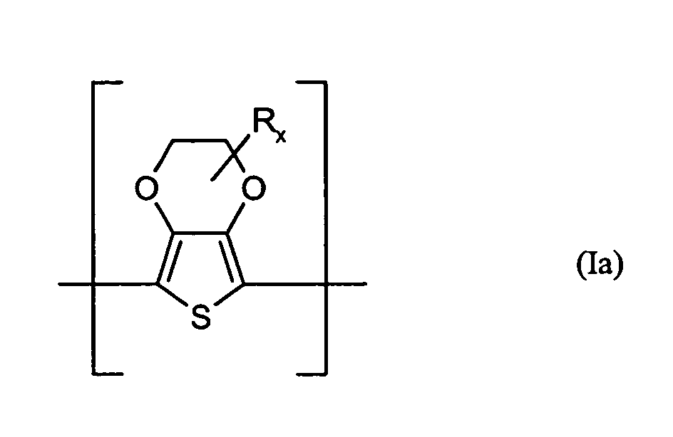
- the layer containing at least one conductive polymer containing a layer at least one polymeric anion and at least one polythiophene with repeating units of the general formula (I) applied.
- Preferred conductive polymers are optionally substituted polythiophenes, polypyrroles or Polyanilines, particularly preferred are polythiophenes having repeating units of the general Formula (I).
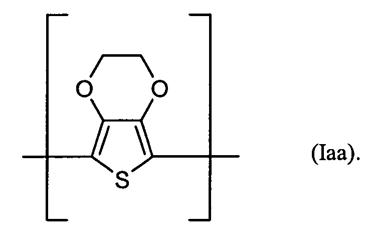
- polythiophenes are those having recurring units of the general formula (Iaa)
- the prefix poly- is to be understood as meaning that more than one or the same containing various repeating unit in the polymer or polythiophene.
- the polythiophene contain a total of n repeating units of the general formula (I), where n is in particular may be an integer from 2 to 2000, preferably from 2 to 100.
- the recurring Units of the general formula (I) may be the same within or within a polythiophene to be different. Preference is given to polythiophenes having in each case the same recurring units the general formula (I).
- the polythiophenes preferably carry H.
- the polythiophene is with repeating units of the general formula (I) poly (3,4-ethylenedioxythiophene), i. a homopolythiophene repeating units of the formula (Iaa).
- C 1 -C 5 -alkylene radicals A are in the context of the invention: methylene, ethylene, n-propylene, n-butylene or n-pentylene.
- C 1 -C 18 -alkyl in the context of the invention is linear or branched C 1 -C 18 -alkyl radicals, for example methyl, ethyl, n- or isopropyl, n-, iso-, sec- or tert-butyl, n -Pentyl, 1-methylbutyl, 2-methylbutyl, 3-methylbutyl, 1-ethylpropyl, 1,1-dimethylpropyl, 1,2-dimethylpropyl, 2,2-dimethylpropyl, n-hexyl, n-heptyl, n-octyl, 2 Ethylhexyl, n-nonyl, n-decyl, n-undecyl,
- substituents of the C 1 -C 5 -alkylene radicals A are numerous organic groups, for example alkyl, cycloalkyl, aryl, halogen, ether, thioether, disulfide, sulfoxide, sulfone, sulfonate , Amino, aldehyde, keto, carboxylic ester, carboxylic acid, carbonate, carboxylate, cyano, alkylsilane and alkoxysilane groups and carboxylamide groups.
- Preferred polymeric anions are, for example, anions of polymeric carboxylic acids, such as polyacrylic acids, Polymethacrylic acid or polymaleic acids, or polymeric sulfonic acids, such as polystyrenesulfonic acids and polyvinylsulfonic acids.
- polymeric carboxylic acids such as polyacrylic acids, Polymethacrylic acid or polymaleic acids
- polymeric sulfonic acids such as polystyrenesulfonic acids and polyvinylsulfonic acids.
- These polycarboxylic and sulfonic acids can also Copolymers of vinyl carboxylic and vinyl sulfonic acids with other polymerizable monomers, such as acrylic esters and styrene.
- polystyrene sulfonic acid PSS
- PSS polystyrene sulfonic acid
- the molecular weight of the polyanionic polyacids is preferably 1,000 to 2,000,000, more preferably 2,000 to 500,000.
- the polyacids or their alkali metal salts are in the Commercially available, e.g. Polystyrenesulfonic acids and polyacrylic acids, or according to known Processes can be prepared (see, for example, Houben Weyl, Methods of Organic Chemistry, Vol Macromolecular substances, Part 2, (1987), p 1141 u.f.).
- the conductive polymers or polythiophenes may be neutral or cationic. In preferred Embodiments are cationic, with "cationic" referring only to the charges that sitting on the polymer or polythiophene main chain.
- the polymers or polythiophenes carry positive and negative charges in the structural unit, wherein the positive charges on the polymer or polythiophene main chain and the negative Charges optionally on the radicals substituted by sulfonate or carboxylate groups R are located.
- the positive charges of the polymer or Polythiophenhauptkette partly or wholly by the optionally present anionic groups on the R residues R be saturated.
- the polymers or polythiophenes in these cases may be cationic, neutral or even anionic. Nevertheless, they will be part of the Considered all as cationic polymers or polythiophenes, since the positive charges are relevant on the polymer or polythiophene main chain.
- the positive charges are in The formulas are not shown because their exact number and position can not be determined properly. However, the number of positive charges is at least 1 and at most n, where n is the total number all recurring units (same or different) within the polymer or polythiophene is.
- Suitable polymeric anions are those already mentioned above.
- Examples of monomeric anions are those of C 1 -C 20 -alkanesulfonic acids, such as methane, ethane, propane, butane or higher sulfonic acids, such as dodecanesulfonic acid, of aliphatic perfluorosulfonic acids, such as trifluoromethanesulfonic acid, perfluorobutanesulfonic acid or perfluorooctanesulfonic acid, aliphatic C 1 -C 20 -carboxylic acids such as 2-ethylhexylcarboxylic acid, aliphatic perfluorocarboxylic acids such as trifluoroacetic acid or perfluorooctanoic acid, and aromatic sulfonic acids optionally substituted by C 1 -C 20 -alkyl groups such as benzenesulfonic acid, o-toluenesulfonic acid, p To
- anions of p-toluenesulfonic acid, methanesulfonic acid or Camphor sulfonic acid are particularly preferred.
- Cationic polythiophenes containing anions as counterions for charge compensation are also often referred to in the art as polythiophene / (poly) anion complexes.
- the polymeric anion as counterion act in the layer containing at least one polymeric anion and at least one polythiophene with repeating units of the general formula (I).
- additional counterions may be included in the layer. Prefers however, in this layer, the polymeric anion serves as the counterion.
- Polymer (s) anion (s) and polythiophene (s) may be present in the layer in a weight ratio from 0.5: 1 to 50: 1, preferably from 1: 1 to 30: 1, more preferably 2: 1 to 20: 1 may be included.
- the weight of the polythiophene corresponds to the weight of the monomers used under Assuming that complete conversion takes place in the polymerization.
- the transparent electrode includes a layer of a conductive one Polymer, a polythiophene, polypyrrole or polyaniline, preferably a polythiophene with repeating units of the general formula (I) in which R, A and x are the abovementioned Meaning, to which a second layer of a polymeric anion and a polythiophene with repeating units of the general formula (I) is applied.
- the transparent electrode includes a Layer of poly (3,4-ethylenedioxythiophene) on the one layer of polystyrene sulfonic acid and Poly (3,4-ethylenedioxythiophene), the latter in the art also as PEDT / PSS or PEDT: PSS referred to, is applied.
- the transparent electrode according to the invention can be applied to a substrate.
- a substrate may be, for example, glass, thin glass (flexible glass) or plastics act.
- plastics for the substrate are: polycarbonates, polyesters, e.g. PET and PEN (polyethylene terephthalate or polyethylene naphthalene dicarboxylate), copolycarbonates, polysulfone, Polyethersulfone (PES), polyimide, polyethylene, polypropylene or cyclic polyolefins or cyclic olefin copolymers (COC), hydrogenated styrene polymers or hydrogenated styrene copolymers.
- PET and PEN polyethylene terephthalate or polyethylene naphthalene dicarboxylate
- copolycarbonates polysulfone, Polyethersulfone (PES), polyimide, polyethylene, polypropylene or cyclic polyolefins or cyclic olefin copolymers (COC), hydrogenated styrene polymers or hydrogenated styrene copolymers.
- Suitable polymer substrates for example, films such as polyester films, PES films the company Sumitomo or polycarbonate films from Bayer AG (Makrofol®).
- Adhesion promoters are, for example, silanes. Preference is given to epoxysilanes, such as, for example, 3-glycidoxypropyltrimethoxysilane (Silquest® A187, OSi specialties). There are others Adhesion promoters having hydrophilic surface properties can be used. For example, a thin layer of PEDT: PSS described as a suitable adhesion promoter for PEDT (Hohnholz et al., Chem. Commun. 2001, 2444-2445).
- the electrode of the invention has over the known known transparent described above ITO-free electrodes have the advantage that they have both a good conductivity and a good one Transmission has.
- the preferred subject of the invention is a transparent electrode having a surface resistance the two polymer layers (first conductive and second layer) of smaller or is equal to 1000 ⁇ / sq, more preferably less than or equal to 500 ⁇ / sq, most preferably of less than or equal to 300 ⁇ / sq.
- Transparent in the sense of the invention means transparent to visible light.
- a transparent electrode which has a transmission of Y is greater than or equal to 25, more preferably Y is greater than or equal to 50.
- the Transmission is determined by the method of measurement described in ASTM D 1003-00 is described. The transmission is then according to ASTM E 308 (illuminant C, 2 * observer) certainly.
- the surface roughness of the electrode according to the invention is also advantageously clear smaller than, for example, the electrodes known from EP-A 686 662, so that the short-circuit probability reduced for OLEDs and OSCs with the electrodes according to the invention becomes.
- the electrodes according to the invention may have a surface roughness with a Mean roughness Ra of less than or equal to 3 nm, more preferably of less than or equal to 1.5 nm, very particularly preferably less than or equal to 1 nm.
- the electrodes according to the invention can be prepared in a simple manner by all Electrode layers are applied from solution in succession. In this way, consuming and avoids expensive vapor deposition or sputtering processes.
- the preparation is advantageously carried out such that the layer containing at least one conductive Polymer of precursors for the preparation of conductive polymers, optionally in the form of Solutions directly in situ on a suitable substrate by means of chemical oxidative polymerization in the presence of one or more oxidants or by electropolymerization and, optionally after drying and washing, the layer containing on this layer at least one polymeric anion and at least one polythiophene with repeating units of the general formula (I) from a dispersion containing at least one polymeric anion and at least one polythiophene having recurring units of the general formula (I) is applied becomes.
- Suitable substrates are those already mentioned above in question.
- the substrate can before applying the layer comprising at least one conductive polymer with a coupling agent be treated.
- a treatment can be achieved, for example, by spin coating, impregnation, Pouring, dripping, spraying, spraying, knife coating, brushing or printing, for example Ink-jet, screen, contact or pad printing done.
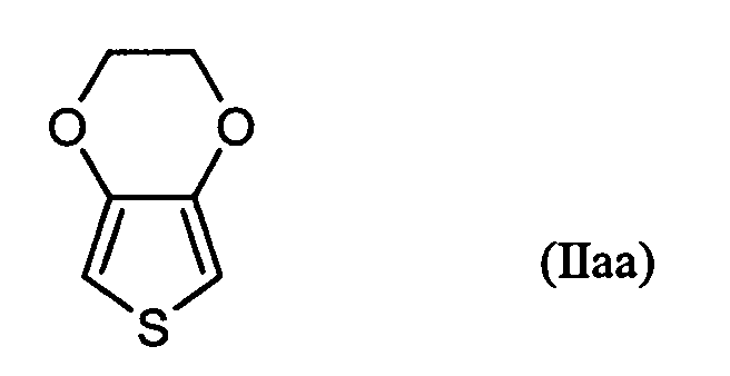
- 3,4-alkylenedioxythiophenes of the formula (IIaa) are used as monomeric precursors. used.
- derivatives of these monomeric precursors are, for example, dimers or trimers of these monomeric precursors understood. They are also higher molecular weight derivatives, i.e. Tetramers, pentamers, etc. of the monomeric precursors as derivatives possible.
- the derivatives can be built from the same or different monomer units and in pure Form as well as mixed with each other and / or with the monomer precursors are used. Oxidized or reduced forms of these precursors are within the meaning of the invention of the
- precursors includes, if in their polymerization, the same conductive polymers arise as in the precursors listed above.
- substituents for the precursors in particular for the thiophenes, preferably for the 3,4-alkylenedioxythiophenes are the radicals mentioned for the general formula (I) for R in question.
- the precursors may optionally be used in the form of solutions.
- Solvents for the precursors are especially inert under the reaction conditions organic solvents called: aliphatic alcohols such as methanol, ethanol, i-propanol and butanol; aliphatic ketones such as acetone and methyl ethyl ketone; aliphatic carboxylic acid esters such as ethyl acetate and butyl acetate; aromatic hydrocarbons such as toluene and xylene; aliphatic hydrocarbons such as hexane, heptane and cyclohexane; Hydrochlorofluorocarbons such as dichloromethane and dichloroethane; aliphatic nitriles such as acetonitrile, aliphatic sulfoxides and sulfones such as dimethylsulfoxide and sulfolane; aliphatic carboxylic acid amides such as methylacetamide
- the solutions may also contain other components such as one or more in organic solvents soluble organic binders such as polyvinyl acetate, polycarbonate, polyvinyl butyral, polyacrylic acid esters, Polymethacrylic acid esters, polystyrene, polyacrylonitrile, polyvinyl chloride, polybutadiene, Polyisoprene, polyethers, polyesters, silicones, styrene / acrylic ester, vinyl acetate / acrylic ester and ethylene / vinyl acetate copolymers or water-soluble binders such as polyvinyl alcohols, Crosslinkers such as polyurethanes or polyurethane dispersions, polyacrylates, polyolefin dispersions, Epoxysilanes such as 3-glycidoxypropyltrialkoxysilane, and / or additives such as e.g. Imidazole or surfactant Substances are added. Furthermore, alkoxysilane hydrolysates, e.g.
- the precursors polymerize chemically oxidatively to the conductive polymers be the presence of one or more oxidizing agents is required.
- oxidizing agent all known to those skilled in the oxidative polymerization of Thiophenes, anilines or pyrroles suitable metal salts are used.
- Suitable metal salts are metal salts of main or subgroup metals, the latter below also referred to as transition metal salts, of the Periodic Table of the Elements.
- suitable Transition metal salts are in particular salts of an inorganic or organic acid or organic acid-containing inorganic acid of transition metals, e.g. of iron (III), Copper (II), chromium (VI), cerium (IV), manganese (IV), manganese (VII) and ruthenium (III).
- Preferred transition metal salts are those of iron (III).
- Ferric salts are often inexpensive, readily available and can be easily handled, such as the ferric salts of inorganic acids, such as ferric halides (eg FeCl 3 ) or ferric salts of others inorganic acids, such as Fe (ClO 4 ) 3 or Fe 2 (SO 4 ) 3 , and the iron (III) salts of organic acids and organic acids containing organic radicals.
- iron (III) salts of organic acids containing inorganic acids are the iron (III) salts of the sulfuric acid monoesters of C 1 -C 20 -alkanols, for example the iron (III) salt of lauryl sulfate.
- transition metal salts are those of an organic acid, in particular Ferric salts of organic acids.
- iron (III) salts of organic acids which may be mentioned are: the iron (III) salts of C 1 -C 20 -alkanesulfonic acids, such as methane, ethane, propane, butane or higher sulfonic acids, such as dodecanesulfonic acid, of aliphatic perfluorosulfonic acids such as trifluoromethanesulfonic acid, perfluorobutanesulfonic acid or perfluorooctanesulfonic acid, aliphatic C 1 -C 20 carboxylic acids such as 2-ethylhexylcarboxylic acid, aliphatic perfluorocarboxylic acids such as trifluoroacetic acid or perfluorooctanoic acid, and aromatic, optionally C 1 -C 20 Alkyl groups substituted sulfonic acids such as benzenesulfonic acid, o-toluenesulfonic acid, p-toluene
- Iron (III) p-toluenesulfonate, iron (III) o-toluenesulfonate are very particularly preferred as metal salts or a mixture of iron (III) p-toluenesulfonate and iron (III) -o-toluenesulfonate.
- the metal salts are prior to their use with an ion exchanger, preferably a basic anion exchanger.
- an ion exchanger preferably a basic anion exchanger.
- suitable Ion exchangers are macroporous polymers functionalized with tertiary amines Styrene and divinylbenzene as described e.g. under the trade name Lewatit® from Bayer AG, Leverkusen to be expelled.
- peroxo compounds such as peroxodisulfates (persulfates), in particular ammonium and alkali peroxodisulfates, such as sodium and potassium peroxodisulfate, or alkali metal perborates - optionally in the presence of catalytic amounts of metal ions, such as Iron, cobalt, nickel, molybdenum or vanadium ions, as well as transition metal oxides, e.g. Manganese (manganese (IV) oxide) or cerium (IV) oxide.
- peroxodisulfates persulfates
- ammonium and alkali peroxodisulfates such as sodium and potassium peroxodisulfate
- alkali metal perborates optionally in the presence of catalytic amounts of metal ions, such as Iron, cobalt, nickel, molybdenum or vanadium ions, as well as transition metal oxides, e.g. Manganese (manganese (IV) oxide) or cerium
- oxidative polymerization of the thiophenes of the formula (II) are theoretically per mole of thiophene 2.25 equivalents of oxidizing agent is required (see, for example, J. Polym., Sc., Part A Polymer Chemistry Vol. 26, p. 1287 (1988)). But it can also lower or higher equivalents of oxidizing agent be used. Within the scope of the invention, one mole of thiophene is preferred Equivalent or more, more preferably 2 equivalents or more of oxidizing agent used.
- the anions of the oxidizing agent used can serve as counterions, so that in the case of chemical oxidative polymerization, addition of additional counterions is not is mandatory.
- the oxidizing agents may be used together with or separately from the precursors - optionally in Form of solutions - applied to the substrate.
- the substrate is preferably first with the solution of the oxidizing agent and optionally the counterions and then coated with the precursor solution.
- oxidants and optionally counterions become the oxide layer of the anode body only with one, namely a thiophene, oxidizing agent and optionally counterions coated solution containing.
- solvents come in all cases, the above as suitable for the precursors described in question.
- the solutions can also be used as other components of the above already for the solutions contain the precursors described components (binders, crosslinkers, etc.).
- the solutions to be applied to the substrate preferably contain from 1 to 30% by weight of the precursors, preferably the thiophenes of the general formula (I) and optionally 0 to 50% by weight % Binders, crosslinkers and / or additives, both percentages by weight based on the total weight the mixture.
- the solutions are prepared by known methods, e.g. by spincoating, impregnation, pouring, dripping, Spraying, spraying, knife coating, painting or printing, for example ink-jet, Screen or pad printing applied to the substrate.
- any solvent present after application of the solutions can be done by simply evaporating at room temperature. To achieve higher processing speeds however, it is more advantageous to use the solvents at elevated temperatures, e.g. at temperatures of 20 to 300 ° C, preferably 40 to 250 ° C to remove.
- a Thermal aftertreatment can be directly associated with the removal of the solvent or else be made at a time interval from the completion of the coating.
- the solvents can be removed before, during or after the polymerization.
- the duration of the heat treatment may vary depending on the type of coating used Polymers 5 seconds to several hours amount.
- Polymers 5 seconds to several hours amount For the thermal treatment Temperature profiles with different temperatures and residence times can also be used become.
- the heat treatment may e.g. be carried out in such a way that the coated one Substrates at such a speed by a located at the desired temperature Heat chamber moves that reaches the desired residence time at the selected temperature or with a hotplate at the desired temperature for the desired Dwell time brings into contact.
- the heat treatment may be, for example take place in a heating furnace or several furnaces each with different temperatures.
- a suitable solvent preferably water or alcohols
- residual salts are here the salts of the reduced form of the oxidizing agent and optionally to understand other available salts.
- the alternative electrochemical polymerization may be by methods known to those skilled in the art be performed.
- the monomers, in particular the thiophenes of the general formula (II) are liquid, can the electropolymerization in the presence or absence of under the conditions of electropolymerization inert solvents are made; the electropolymerization of solid in particular thiophenes of the general formula (II) is in the presence of below the conditions of electrochemical polymerization inert solvents.
- solvent mixtures and / or the solvents Add solubilizers (detergents).
- the electropolymerization inert solvents are, for example called: water; Alcohols such as methanol and ethanol; Ketones such as acetophenone; halogenated Hydrocarbons such as methylene chloride, chloroform, carbon tetrachloride and fluorocarbons; Esters such as ethyl acetate and butyl acetate; Carbonic acid esters such as propylene carbonate; aromatic Hydrocarbons such as benzene, toluene, xylene; aliphatic hydrocarbons such Pentane, hexane, heptane and cyclohexane; Nitriles such as acetonitrile and benzonitrile; Sulfoxides like dimethyl sulfoxide; Sulfones such as dimethylsulfone, phenylmethylsulfone and sulfolane; liquid aliphatic Amides such as methylacetamide, dimethylacetamide, dimethylformamide
- the monomers are in particular the thiophenes of the general Formula (II) or their solutions added with electrolyte additives.
- electrolyte additives are preferably uses free acids or common conductive salts which have a certain solubility in the have used solvents.
- electrolyte additives e.g.
- free acids such as p-toluenesulfonic acid, methanesulfonic acid, furthermore salts with alkanesulfonate, aromatic Sulfonate, tetrafluoroborate, hexafluorophosphate, perchlorate, hexafluoroantimonate, hexafluoroarsenate and hexachloroantimonate anions and alkali, alkaline earth or optionally alkylated ammonium, phosphonium, sulfonium and oxonium cations.
- the concentration of the monomers, in particular the thiophenes of the general formula (II) can between 0.01 and 100 wt.% (100 wt.% only with liquid thiophene); prefers the concentration is 0.1 to 20 wt .-%, based on the total weight of the solution.
- the electropolymerization may be carried out batchwise or continuously.
- the current density for the electropolymerization can vary within wide limits; Usually, a current density of 0.0001 to 100 mA / cm 2 , preferably 0.01 to 40 mA / cm 2 is used. At these current densities, a voltage of about 0.1 to 50 V sets.
- Suitable counterions are those already listed above.
- these counterions of the solution or the thiophenes may be added as electrolyte additives or conductive salts are added.
- the electrochemical oxidative polymerization of the thiophenes of the general formula (II) can at a temperature of -78 ° C to the boiling point of the solvent optionally used be made. Preference is given at a temperature of -78 ° C to 250 ° C, particularly preferred from -20 ° C to 60 ° C electrochemically polymerized.
- reaction times are dependent on the thiophene used, the electrolyte used, the selected temperature and the applied current density preferably 1 minute up to 24 hours.
- the substrate which is usually not conductive
- first as in Groenendaal et al. Adv.Mat. 2003, 15, 855 can be coated with a thin transparent layer of a conductive polymer.
- the conductive substrate coated with a surface resistance of ⁇ 10 4 ⁇ / sq takes over the function of the Pt electrode in the subsequent electropolymerization.
- the layer containing the conductive polymer grows upon application of a stress thereon.
- the conductive polymer (s) in the layer containing at least one conductive polymer can be generated directly by polymerization of precursors in situ on the substrate, In the following, this layer is also referred to as "in-situ layer".
- in-situ layer The concept of in-situ deposition a conductive polymer of a polymerizable solution of monomer and Oxidizing agent is well known in the art.
- a layer containing at least one polymeric anion and at least one optionally substituted polyaniline and / or at least one polythiophene with repeating units of the general formula (I) from a dispersion containing at least a polymeric anion and at least one optionally substituted polyaniline and / or at least one polythiophene having repeating units of the general formula (I) applied.
- a layer comprising at least one polymeric anion is applied to the in-situ layer and at least one polythiophene having repeating units of the general formula (I) a dispersion containing at least one polymeric anion and at least one polythiophene with repeating units of the general formula (I) applied.
- the dispersions may also contain one or more solvents.
- a solvent are the above already mentioned for the precursors in question.
- Preferred solvents are water or other protic solvents such as alcohols, e.g. Methanol, ethanol, i-propanol and butanol, as well as mixtures of water with these alcohols, most preferred Solvent is water.
- the dispersion is solidified to form the second layer, especially solvent-containing Dispersions by removal of the solvent or by oxidative crosslinking, preferably by exposing the dispersion layer to (air) oxygen.
- Suitable polymeric anions are those already mentioned above. preferred ranges apply analogously.
- the dispersions are prepared from thiophenes of the general formula (II), for example analogous to the conditions mentioned in EP-A 440 957.
- oxidizing agent solvent and polymeric anions are those already mentioned above in question.
- the dispersions are prepared by known methods, e.g. by spincoating, impregnation, casting, Dripping, spraying, spraying, knife coating, brushing or printing, for example ink-jet, Screen or pad printing applied to the in-situ layer.
- the layer containing at least one polymeric anion and at least a polythiophene having repeating units of the general formula (I) may undergo drying and / or cleaning the layer by washing - as previously described for the in-situ layer described - connect.
- a transparent electrode can be produced without consuming and expensive Aufdampf- or Aufsputter compiler are necessary. This will be under also allows a large-scale application of the method according to the invention. Furthermore both in-situ layer and the polythiophene / polyanion layer can be at low Apply temperatures, preferably room temperature.
- the inventive method is therefore also suitable for application to polymeric, flexible substrates, which are usually only Tolerate low temperature processes and can not withstand the temperatures during ITO deposition.
- the electrodes according to the invention are outstandingly suitable as electrodes in electrical and preferably in electro-optical constructions, in particular in organic light-emitting diodes (OLED), Organic Solar Cell (OSC) Liquid Crystal Displays (LCD) and Optical Sensors.
- OLED organic light-emitting diodes
- OSC Organic Solar Cell
- LCD Liquid Crystal Displays
- Electro-optical structures usually contain two electrodes, at least one of which is translucent is, and in between an electro-optically active layer system.
- the electro-optical structure is an electroluminescent layer arrangement, in the following also briefly as an electroluminescent device or EL device referred to as.
- the simplest case of such an EL device consists of two electrodes, of which at least one is transparent, and one electro-optically active layer between these two electrodes.
- other functional layers in such an electroluminescent Layer structure may be included, such. charge-injecting, charge-transporting or charge-blocking intermediate layers.
- Such layer structures are known to the person skilled in the art and, for example, in (J.R.Sheats et al., Science 273, (1996), 884).
- a layer can also take on several tasks.
- the electro-optically active, i. usually light-emitting, layer the functions take over the other layers.
- One of the two electrodes or both electrodes can onto a suitable substrate, i. a suitable carrier applied. The layer structure is then contacted and optionally wrapped and / or encapsulated.
- the construction of multilayer systems can be achieved by vapor deposition ("Chemical Vapor deposition ", CVD), in which the layers are applied successively from the gas phase, or done by casting.
- the vapor deposition methods are used in conjunction with the hole mask technique used for the fabrication of structured LEDs that emit organic molecules to use. Casting processes are due to the higher process speeds and the lower Amount of rejects produced and associated cost savings in general prefers.
- the electrodes according to the invention can be advantageously - as already described above from solution / dispersion
- Another object of the present invention is therefore an electroluminescent device consisting of at least two electrodes, of which at least one electrode is transparent, and an electro-optically active layer between the electrodes, characterized in that it contains an electrode according to the invention as a transparent electrode.
- Preferred electroluminescent devices are those which are suitable for use on a suitable substrate applied electrode according to the invention, i. in-situ layer and layer containing at least a polymeric anion and at least one polythiophene of the general formula (I), a Emitter layer and a metal cathode included.
- the layer containing at least one polymeric anion and at least one polythiophene of the general formula (I) act as a hole-injecting intermediate layer.
- other functional layers listed above may be included.
- the electrically conductive layer is in particular made with a plurality of electrically highly conductive metallic Supply lines contacted as anode.
- Active matrix substrates are usually non-transparent Si layers in which a transistor was processed under each light pixel.
- Suitable emitter materials and materials for metal cathodes are common to electro-optical structures and known in the art.
- the metal cathode are preferably those of low work function metals such as Mg, Ca, Ba or metal salts such as LiF into consideration.
- Preferred emitter materials are conjugated polymers such as polyphenylenevinylenes or polyfluorenes or emitters from the class of low molecular weight emitters, also referred to in the art as "small molecules", such as tris (8-hydroxyquinolinato) aluminum (Alq 3 ).
- a transparent electrode of an in-situ layer alone shows a significant disadvantage Applications in OLEDs, since the achievable luminous efficacy is very low.
- This layer can be very thin and have a high resistivity because of the Light emission necessary device current flows through the underlying in-situ layer.
- Electrodes of a polythiophene / polyanion layer, in particular of a PEDT: PSS layer alone are in contrast to the above-described double layer according to the invention due to too low conductivity or too coarse particle structure for applications in OLEDs or OSCs also poorly suited.
- suitable PEDT: PSS formulations have a composition of PEDT: PSS like 1: 6 or 1:20 and are characterized by a lot fine particle structure. The surface resistance of a 100 nm thick layer of these
- PEDT PSS formulation with higher PEDT content, such as e.g. with PEDT: PSS of 1: 2.5, can be achieved by adding additives such as N-methyl-pyrrolidone, Although sorbitol or glycerol increase so that surface resistances of approx. 10 k ⁇ / sq at a layer thickness of 100 nm can be achieved, however, even with these more conductive PEDT: PSS formulations alone not in the double layer according to the invention achievable surface resistivities of less than 1000 ⁇ / sq at 100 nm layer thickness.
- Another disadvantage of the formulations with a higher PEDT content is the coarse one Particle structure and the associated higher short-circuit probability for OLEDs and OSCs.
- a special electrode according to the invention with a 100 nm thick in situ PEDT layer and an overlying PEDT: PSS layer (PEDT: PSS ratio as in the previous section)
- PEDT PSS ratio as in the previous section
- the electrode of the invention significantly improves the efficiency of the electro-optical structure.
- bus-bars To the voltage drop between anode pad and OLED anode particularly small too as described above, highly conductive leads, for example of metals, so-called “bus-bars" are used.
- ITO address lines be waived. In their place take over metallic supply lines (bus bars) in combination with electrode according to the invention, the anode-side addressing (see Fig.1).
- a transparent Carrier 1 e.g. a glass plate
- electric leads 2a and pixel frames 2b are included high conductivity applied. This could e.g. by steaming metals or inexpensively be applied by printing with metal pastes.
- the polymeric Electrode layer 3 deposited.
- an adhesion promoter as second layer the in-situ layer and as third layer the polythiophene (s) and polymer (s) Anion (s) containing layer applied.
- the application of these layers is preferably carried out through spin-coating, printing and ink-jetting.
- the further structure corresponds to that of a standard Passive matrix OLED and is known in the art.
- OLEDs In the case of homogeneously luminous OLEDs (OLED lamps) can be due to the invention on ITO electrodes be waived. In their place take over metallic supply lines (bus bars) in Combination with electrode according to the invention the function of the whole-area anode (see Fig.2).
- a transparent support e.g. a glass plate
- electrical leads 2 are high Conductivity, for example, applied as described in the previous section.
- the polymeric electrode layer is formed 3 deposited.
- the further structure corresponds to that of a standard OLED lamp.
- ITO-coated glass substrates (Merck Display) are cut to a size of 50 x 50 mm 2 and cleaned. Thereafter, the ITO coating is coated with photopositive varnish (available from JSR, LCPR 1400G-80cP) and this is exposed after drying through a printed polymer film (shadow mask).
- the shadow mask consists of isolated translucent circles with 5 mm diameter, which are arranged square at a distance of 10 mm. After exposure and drying, the uncrosslinked photoresist is removed from the circular areas with the developer solution (available from JSR, TMA238WA).
- the ITO is subsequently treated with an etching solution consisting of 47.5% by volume of deionized (dist.) Water, 47.5% by volume hydrochloric acid (32%), 5.0% by volume. Nitric acid (65%), removed.
- the crosslinked photoresist is then removed with acetone and the structured ITO substrate is finally cleaned.
- Epoxysilane (Silquest® A187, OSi specialties) is diluted with 20 parts of 2-propanol spin coated on the cleaned, structured ITO substrate with a spin coater and then dried at 50 ° C for 5 min in air.
- the layer thickness is less than 20 nm.
- a solution consisting of Baytron® M, Baytron® CB 40 and imidazole im Weight ratio 1: 20: 0.5 is prepared and filtered (Millipore HV, 0.45 microns). In connection the solution is patterned onto the epoxysilane coated with a spin coater ITO substrate spun at 1000 rpm. Then the layer is added Room temperature (RT, 23 ° C) and then dried with dist. Rinsed water carefully, to remove the iron salts. After drying the layers in a rotary dryer the layer thickness is about 150 nm.
- the surface roughness Ra is about 5 nm
- Conductivity is 550 S / cm.
- Metal electrodes are evaporated on the organic layer system.
- the used for it Vaporization system (Edwards) is integrated in an inert gas glovebox (brown).
- the Substrate is placed with the organic layer down on a shadow mask.
- the vapor deposition rates are 10 ⁇ / sec for Ca and 20 ⁇ / sec for Ag.
- the two electrodes of the OLED are connected via electrical Feeds connected to a voltage source.
- the positive pole is with the whole area ITO layer
- the negative pole is connected to one of the deposited metal electrodes.
- the unclaimed ITO serves only as a low-resistance one electrical feed for the in-situ PEDT layer.
- the dependence of the OLED current and the electroluminescence intensity (EL) on the voltage are recorded.
- the detection of the EL is done with a photodiode (EG & G C30809E) and the calibration of the luminance with a luminance meter (Minolta LS-100).
- OLEDs with a luminous area of at least 0.049 cm 2 in terms of luminance and efficiency are independent of whether ITO is below the in-situ PEDT layer or not. Furthermore, it is shown by comparing Examples 1 and 2 that a PEDT: PSS layer between the in-situ and the MEH-PPV layer (emitter layer) significantly improves the luminance.
- OLEDs with a luminous area of at least 0.049 cm 2 in terms of luminance and efficiency are independent of whether ITO is below the in-situ PEDT layer or not. Furthermore, it is shown by comparing Examples 3 and 4 that a PEDT: PSS layer between the in-situ and the PF-F8 layer (emitter layer) significantly increases the luminance and lowers the voltage.
Landscapes
- Chemical & Material Sciences (AREA)
- Engineering & Computer Science (AREA)
- Materials Engineering (AREA)
- Physics & Mathematics (AREA)
- Optics & Photonics (AREA)
- Organic Chemistry (AREA)
- Polyoxymethylene Polymers And Polymers With Carbon-To-Carbon Bonds (AREA)
- Non-Insulated Conductors (AREA)
- Electroluminescent Light Sources (AREA)
- Hybrid Cells (AREA)
- Liquid Crystal (AREA)
- Photovoltaic Devices (AREA)
- Laminated Bodies (AREA)
Abstract
Description

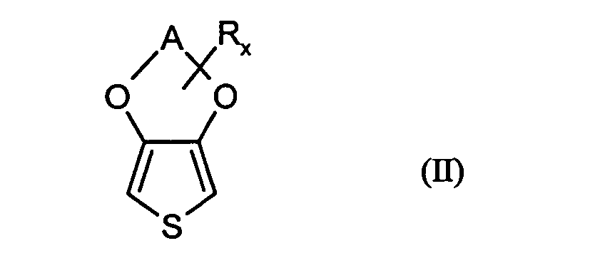
- A
- für einen gegebenenfalls substituierten C1-C5-Alkylenrest, bevorzugt für einen gegebenenfalls substituierten C2-C3-Alkylenrest, steht,
- R
- für einen linearen oder verzweigten, gegebenenfalls substituierten C1-C18-Alkylrest, bevorzugt linearen oder verzweigten, gegebenenfalls substituierten C1-C14-Alkylrest, einen gegebenenfalls substituierten C5-C12-Cycloalkylrest, einen gegebenenfalls substituierten C6- C14-Arylrest, einen gegebenenfalls substituierten C7-C18-Aralkylrest, einen gegebenenfalls substituierten C1-C4-Hydroxyalkylrest, bevorzugt gegebenenfalls substituierten C1-C2-Hydroxyalkylrest, oder einen Hydroxylrest steht,
- x
- für eine ganze Zahl von 0 bis 8 steht, bevorzugt von 0 bis 6, besonders bevorzugt für 0 oder 1 steht und
- R und x
- die oben genannte Bedeutung haben.
eine erste Schicht enthaltend wenigstens ein leitfähiges Polymer hergestellt wird, indem auf ein Substrat Vorstufen zur Herstellung leitfähiger Polymere gegebenenfalls in Form von Lösungen aufgebracht werden und chemisch oxidativ in Gegenwart eines oder mehrerer Oxidationsmittel oder elektrochemisch zu den leitfähigen Polymeren polymerisiert werden, und
gegebenenfalls nach Waschen und Trocknung auf diese Schicht eine zweite Schicht enthaltend wenigstens ein polymeres Anion und wenigstens ein gegebenenfalls substituiertes Polyanilin und/oder wenigstens ein Polythiophen mit wiederkehrenden Einheiten der allgemeinen Formel (I)

- A, R und x
- die oben zu Formel (I) genannte Bedeutung haben,

- A, R und x
- die oben genannte Bedeutung haben,

| OLED-Aufbau | Stromdichte [mA/cm2] | Spannung [V] | Leuchtdichte [cd/m2] | Effizienz [cd/A] |
| ITO//In-Situ-PEDT// PEDT:PSS//MEH-PPV//Ca//Ag (vgl. Beispiel 1) | 102 | 5.1 | 105 | 0.10 |
| In-Situ-PEDT//PEDT:PSS// MEHPPV//Ca//Ag (vgl. Beispiel 1) | 102 | 6.0 | 102 | 0.10 |
| ITO//In-Situ-PEDT// MEH-PPV//Ca//Ag (vgl. Beispiel 2) | 102 | 6.6 | 19 | 0.019 |
| In-Situ-PEDT//MEH-PPV//Ca//Ag (vgl. Beispiel 2) | 102 | 6.3 | 16 | 0.016 |
| OLED-Aufbau | Stromdichte [mA/cm2] | Spannung [V] | Leuchtdichte [cd/m2] | Effizienz [cd/A] |
| ITO//In-Situ-PEDT//PEDT:PSS// PFF8//Ca//Ag (vgl. Beispiel 3) | 204 | 6.9 | 28 | 0.014 |
| In-Situ-PEDT// PEDT:PSS//PF-F8// Ca//Ag (vgl. Beispiel 3) | 204 | 7.4 | 23 | 0.010 |
| ITO//In-Situ-PEDT//PF-F8//Ca//Ag (vgl. Beispiel 4) | 204 | 9.5 | 2,5 | 0.0012 |
| In-Situ-PEDT//PF-F8//Ca//Ag (vgl. Beispiel 4) | 204 | 9.3 | 2,3 | 0.0011 |
Claims (20)
- Transparente Elektrode, dadurch gekennzeichnet, dass sie eine erste Schicht enthaltend wenigstens ein leitfähiges Polymer enthält, auf die eine zweite Schicht enthaltend wenigstens ein polymeres Anion und wenigstens ein gegebenenfalls substituiertes Polyanilin und/oder wenigstens ein Polythiophen mit wiederkehrenden Einheiten der allgemeinen Formel (I),worin
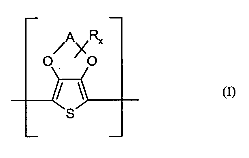 für den Fall, dass mehrere Reste R an A gebunden sind, diese gleich oder unterschiedlich sein können,A für einen gegebenenfalls substituierten C1-C5-Alkylenrest steht,R für einen linearen oder verzweigten, gegebenenfalls substituierten C1-C18-Alkylrest, einen gegebenenfalls substituierten C5-C12-Cycloalkylrest, einen gegebenenfalls substituierten C6-C14-Arylrest, einen gegebenenfalls substituierten C7-C18-Aralkylrest, einen gegebenenfalls substituierten C1-C4-Hydroxyalkylrest oder einen Hydroxylrest steht,x für eine ganze Zahl von 0 bis 8 steht und
aufgebracht ist. - Elektrode gemäß Anspruch 1, dadurch gekennzeichnet, dass das leitfähige Polymer ein gegebenenfalls substituiertes Polythiophen, Polypyrrol oder Polyanilin ist.
- Elektrode gemäß Anspruch 1 oder 2, dadurch gekennzeichnet, dass das leitfähige Polymer ein Polythiophen mit wiederkehrenden Einheiten der allgemeinen Formel (I) ist, wobei A, R und x die in Anspruch 1 angegebene Bedeutung tragen.
- Elektrode gemäß wenigstens einem der Ansprüche 1 bis 3, dadurch gekennzeichnet, dass in Formel (I) für das leitfähige Polymer und das Polythiophen der zweiten Schicht unabhängig voneinander A für einen gegebenenfalls substituierten C2-C3-Alkylenrest und x für 0 oder 1 steht.
- Elektrode gemäß wenigstens einem der Ansprüche 1 bis 4, dadurch gekennzeichnet, dass das Polythiophen mit wiederkehrenden Einheiten der allgemeinen Formel (I) für das leitfähige Polymer und das Polythiophen der zweiten Schicht unabhängig voneinander Poly(3,4-ethylendioxythiophen) ist.
- Elektrode gemäß wenigstens einem der Ansprüche 1 bis 5, dadurch gekennzeichnet, dass das polymere Anion ein Anion einer polymeren Carbon- oder Sulfonsäure ist.
- Elektrode gemäß wenigstens einem der Ansprüche 1 bis 6, dadurch gekennzeichnet, dass das polymere Anion ein Anion der Polystyrolsulfonsäure ist.
- Elektrode gemäß wenigstens einem der Ansprüche 1 bis 7, dadurch gekennzeichnet, dass die beiden Schichten einen Oberflächenwiderstand von ≤1000 Ω/sq aufweisen.
- Elektrode gemäß wenigstens einem der Ansprüche 1 bis 8, dadurch gekennzeichnet, dass sie eine Transmission von gemessen nach ASTM D 1003-00 in Verbindung mit ASTM E 308 Y ≥25 aufweist.
- Verfahren zur Herstellung einer transparenten Elektrode insbesondere gemäß wenigstens einem der Ansprüche 1 bis 9, dadurch gekennzeichnet, dasseine erste Schicht enthaltend wenigstens ein leitfähiges Polymer hergestellt wird indem auf ein Substrat Vorstufen zur Herstellung leitfähiger Polymere gegebenenfalls in Form von Lösungen aufgebracht werden und chemisch oxidativ in Gegenwart eines oder mehrerer Oxidationsmittel oder elektrochemisch zu den leitfähigen Polymeren polymerisiert werden, undauf diese Schicht nach Waschen und Trocknung gegebenenfalls eine zweite Schicht enthaltend wenigstens ein polymeres Anion und wenigstens ein gegebenenfalls substituiertes Polyanilin und/oder wenigstens ein Polythiophen mit wiederkehrenden Einheiten der allgemeinen Formel (I)worin
 A, R und x die in Anspruch 1 genannte Bedeutung haben,und durch Aufbringen einer lösungsmittelhaltigen Dispersion enthaltend wenigstens ein polymeres Anion und wenigstens ein gegebenenfalls substituiertes Polyanilin und/oder wenigstens ein Polythiophen mit wiederkehrenden Einheiten der allgemeinen Formel (I) auf die elektrisch leitfähige Schicht und anschließendes Verfestigen der Dispersion gegebenenfalls durch Entfernen des Lösungsmittels oder Vernetzer der Dispersion aufgebracht wird.
 - Verfahren gemäß Anspruch 10, dadurch gekennzeichnet, dass das Substrat vor Aufbringen der Schicht enthaltend wenigstens ein leitfähiges Polymer mit einem Haftvermittler behandelt wird.
- Verfahren gemäß Anspruch 10 oder 11, dadurch gekennzeichnet, dass als Vorstufen zur Herstellung leitfähiger Polymere gegebenenfalls substituierte Thiophene, Pyrrole oder Aniline eingesetzt werden.
- Verfahren gemäß wenigstens einem der Ansprüche 10 bis 12, dadurch gekennzeichnet, dass als Vorstufen zur Herstellung leitfähiger Polymere Thiophene der allgemeinen Formel (II),worin
 eingesetzt werden.A, R und x die in Anspruch 1 genannte Bedeutung haben,
 - Verfahren gemäß wenigstens einem der Ansprüche 10 bis 13, dadurch gekennzeichnet, dass als Vorstufen zur Herstellung leitfähiger Polymere Thiophene der allgemeinen Formel (IIa),worin
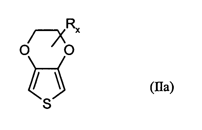 eingesetzt werden.R und x die in Anspruch 1 oder 4 genannte Bedeutung haben,
 - Verfahren gemäß wenigstens einem der Ansprüche 10 bis 14, dadurch gekennzeichnet, dass die Dispersion enthaltend wenigstens ein polymeres Anion und wenigstens ein gegebenenfalls substituiertes Polyanilin und/oder wenigstens ein Polythiophen mit wiederkehrenden Einheiten der allgemeinen Formel (I) als Lösungsmittel organische Lösungsmittel, Wasser oder Mischungen aus diesen enthalten.
- Verfahren gemäß wenigstens einem der Ansprüche 10 bis 15, dadurch gekennzeichnet, dass die Vorstufen zur Herstellung leitfähiger Polymere chemisch oxidativ in Gegenwart eines oder mehrerer Oxidationsmittel zu den leitfähigen Polymeren polymerisiert werden.
- Verwendung der Elektrode gemäß wenigstens einem der Ansprüche 1 bis 9 als transparente Elektrode in elektrooptischen Aufbauten.
- Verwendung der Elektrode gemäß Anspruch 1 bis 9 als transparente Elektrode in organischen Leuchtdioden, organischen Solarzellen, Flüssigkristallanzeigen (LCD) und optischen Sensoren.
- Elektrolumineszierende Anordnung bestehend wenigstens aus zwei Elektroden, von denen mindestens eine transparent ist, und einer elektrooptisch aktiven Schicht zwischen diesen Elekroden dadurch gekennzeichnet, dass sie als transparente Elektrode eine Elektrode gemäß wenigstens einem der Ansprüche 1 bis 9 enthält.
- Elektrolumineszierende Anordnung gemäß Anspruch 19, dadurch gekennzeichnet, dass sie anodenseitig hochleitfähige metallische Zuleitungen enthält.
Applications Claiming Priority (2)
| Application Number | Priority Date | Filing Date | Title |
|---|---|---|---|
| DE10335727 | 2003-08-05 | ||
| DE10335727A DE10335727A1 (de) | 2003-08-05 | 2003-08-05 | Transparente Elektrode für elektro-optische Aufbauten |
Publications (3)
| Publication Number | Publication Date |
|---|---|
| EP1505664A2 true EP1505664A2 (de) | 2005-02-09 |
| EP1505664A3 EP1505664A3 (de) | 2008-07-23 |
| EP1505664B1 EP1505664B1 (de) | 2015-09-23 |
Family
ID=33547074
Family Applications (1)
| Application Number | Title | Priority Date | Filing Date |
|---|---|---|---|
| EP04017458.3A Expired - Lifetime EP1505664B1 (de) | 2003-08-05 | 2004-07-23 | Transparente Elektrode für elektro-optische Aufbauten |
Country Status (6)
| Country | Link |
|---|---|
| US (1) | US20050053801A1 (de) |
| EP (1) | EP1505664B1 (de) |
| JP (1) | JP5090616B2 (de) |
| KR (1) | KR101239437B1 (de) |
| DE (1) | DE10335727A1 (de) |
| TW (1) | TWI405837B (de) |
Cited By (5)
| Publication number | Priority date | Publication date | Assignee | Title |
|---|---|---|---|---|
| WO2008098551A3 (de) * | 2007-02-16 | 2008-11-20 | Osram Opto Semiconductors Gmbh | Elektrolumineszentes organisches halbleiterelement und verfahren zur reparatur eines elektrolumineszenten organischen halbleiterelements |
| WO2009053089A1 (de) * | 2007-10-24 | 2009-04-30 | Merck Patent Gmbh | Optoelektronische vorrichtung |
| EP2194594A1 (de) * | 2006-08-14 | 2010-06-09 | Franz Binder GmbH & Co. Elektrische Bauelemente KG | Verfahren zur Herstellung eines dreidimensionalen Bauteils |
| WO2012048823A1 (en) * | 2010-10-12 | 2012-04-19 | Heraeus Precious Metals Gmbh & Co. Kg | Dispersions comprising polythiophenes with a defined content of thiophene monomer |
| EP1929560B1 (de) * | 2005-09-30 | 2016-01-06 | OSRAM OLED GmbH | Neutralisierte anodenpufferschicht zur verbesserung der verarbeitung und leistungsfähigkeiten organischer lichtemittierender bauelemente und deren herstellungsmethode |
Families Citing this family (37)
| Publication number | Priority date | Publication date | Assignee | Title |
|---|---|---|---|---|
| DE102004012319A1 (de) * | 2004-03-11 | 2005-09-22 | H.C. Starck Gmbh | Funktionsschichten für optische Anwendungen auf Basis von Polythiophenen |
| EP1765908A1 (de) * | 2004-04-20 | 2007-03-28 | Nanon A/S | Baseninhibierte oxidative polymerisation von thiophenen und anilinen mit eisen(iii)-salzen |
| DE112005002603A5 (de) | 2004-08-13 | 2007-08-09 | Novaled Gmbh | Schichtanordnung für ein Lichtemittierendes Bauelement |
| US8137788B2 (en) * | 2004-09-29 | 2012-03-20 | Toray Industries, Inc. | Laminated film |
| US7375867B2 (en) * | 2005-03-04 | 2008-05-20 | Infocus Corporation | Transmissive electromechanical light valve and system |
| DE502005002342D1 (de) * | 2005-03-15 | 2008-02-07 | Novaled Ag | Lichtemittierendes Bauelement |
| EP1713136B1 (de) | 2005-04-13 | 2007-12-12 | Novaled AG | Anordnung für eine organische Leuchtdiode vom pin-Typ und Verfahren zum Herstellen |
| US20070085061A1 (en) * | 2005-10-14 | 2007-04-19 | Elder Delwin L | Conductivity enhancement of conductive polymers by solvent exposure |
| DE102005060159A1 (de) * | 2005-12-14 | 2007-06-21 | H. C. Starck Gmbh & Co. Kg | Transparente polymere Elektrode für elektro-optische Aufbauten |
| DE502005004675D1 (de) * | 2005-12-21 | 2008-08-21 | Novaled Ag | Organisches Bauelement |
| DE602006001930D1 (de) * | 2005-12-23 | 2008-09-04 | Novaled Ag | tur von organischen Schichten |
| EP1808909A1 (de) * | 2006-01-11 | 2007-07-18 | Novaled AG | Elekrolumineszente Lichtemissionseinrichtung |
| EP1848049B1 (de) * | 2006-04-19 | 2009-12-09 | Novaled AG | Lichtemittierendes Bauelement |
| US20070278453A1 (en) * | 2006-06-02 | 2007-12-06 | Steffen Zahn | Electrically conductive polymers and method of making electrically conductive polymers |
| US8388790B2 (en) * | 2006-07-21 | 2013-03-05 | Leonhard Kurz Stiftung & Co. Kg | Multilayered body comprising an electroconductive polymer layer and method for the production thereof |
| DE102006033887B4 (de) * | 2006-07-21 | 2015-04-09 | Leonhard Kurz Gmbh & Co. Kg | Verfahren zur Herstellung eines Mehrschichtkörpers mit leitfähiger Polymerschicht |
| JP5162941B2 (ja) * | 2007-04-05 | 2013-03-13 | コニカミノルタホールディングス株式会社 | 透明導電性フィルム及びその製造方法 |
| DE102007019260B4 (de) * | 2007-04-17 | 2020-01-16 | Novaled Gmbh | Nichtflüchtiges organisches Speicherelement |
| KR100887084B1 (ko) | 2007-05-04 | 2009-03-04 | 삼성전자주식회사 | 투명 전도성 고분자 필름용 조성물, 이를 이용한 투명전도성 고분자 필름의 제조방법, 상기 조성물을 이용하여 제조된 투명전도성 고분자 필름 및 이를 포함하는 전기 영동 디스플레이 |
| DE102007048212A1 (de) * | 2007-10-08 | 2009-04-09 | H.C. Starck Gmbh | Verfahren zur Herstellung von Elektrolytkondensatoren mit polymerer Zwischenschicht |
| DE102008036063B4 (de) * | 2008-08-04 | 2017-08-31 | Novaled Gmbh | Organischer Feldeffekt-Transistor |
| DE102008036062B4 (de) | 2008-08-04 | 2015-11-12 | Novaled Ag | Organischer Feldeffekt-Transistor |
| GB2462688B (en) * | 2008-08-22 | 2012-03-07 | Cambridge Display Tech Ltd | Opto-electrical devices and methods of manufacturing the same |
| JP2010080908A (ja) * | 2008-08-29 | 2010-04-08 | Sumitomo Chemical Co Ltd | 有機光電変換素子およびその製造方法 |
| KR101251194B1 (ko) * | 2009-05-19 | 2013-04-08 | 쇼와 덴코 가부시키가이샤 | 전극의 표면 처리 방법 및 전극 및 유기 일렉트로루미네센스 소자의 제조 방법 |
| US8535571B2 (en) | 2009-12-30 | 2013-09-17 | Korea University Research And Business Foundation | Water-soluble electrically conductive polymers |
| WO2011087458A1 (en) * | 2010-01-14 | 2011-07-21 | National University Of Singapore | Superhydrophilic and water-capturing surfaces |
| CN103687900A (zh) * | 2011-08-12 | 2014-03-26 | 三星电子株式会社 | 荧光树脂膜的制造方法以及由此制造的荧光树脂膜 |
| JP2013045613A (ja) * | 2011-08-24 | 2013-03-04 | Konica Minolta Business Technologies Inc | 色素増感型太陽電池 |
| KR101188747B1 (ko) * | 2012-07-18 | 2012-10-10 | 지스마트 주식회사 | 투명전광판 및 그 제조방법 |
| JP6201317B2 (ja) * | 2012-12-28 | 2017-09-27 | 日本ゼオン株式会社 | 色素増感型光電変換素子および色素増感型太陽電池 |
| WO2014162932A1 (ja) * | 2013-04-01 | 2014-10-09 | パイオニア株式会社 | 光学装置 |
| JP6283022B2 (ja) * | 2013-04-01 | 2018-02-21 | パイオニア株式会社 | 光学装置 |
| JP6266599B2 (ja) * | 2013-04-01 | 2018-01-24 | パイオニア株式会社 | 光学装置 |
| CN110945416B (zh) * | 2017-07-27 | 2022-08-26 | 日产化学株式会社 | 树脂组合物、树脂膜及液晶表示元件 |
| FR3098982B1 (fr) * | 2019-07-19 | 2022-04-15 | Isorg | Dispositif optoélectronique comprenant une couche organique active à performances améliorées et son procédé de fabrication |
| US12492303B2 (en) * | 2021-06-08 | 2025-12-09 | Agfa-Gevaert Nv | Polythiophene/polyanion compositions |
Family Cites Families (14)
| Publication number | Priority date | Publication date | Assignee | Title |
|---|---|---|---|---|
| EP0440957B1 (de) * | 1990-02-08 | 1996-03-27 | Bayer Ag | Neue Polythiophen-Dispersionen, ihre Herstellung und ihre Verwendung |
| JPH0762276A (ja) * | 1993-08-25 | 1995-03-07 | Bridgestone Corp | 導電性高分子複合材料及びその製造方法 |
| DE19507413A1 (de) * | 1994-05-06 | 1995-11-09 | Bayer Ag | Leitfähige Beschichtungen |
| JP2001506393A (ja) * | 1994-09-06 | 2001-05-15 | フィリップス エレクトロニクス ネムローゼ フェンノートシャップ | 導電性ポリマー製の透明な構造を付与した電極層を有するエレクトロルミネセント装置 |
| DE19627071A1 (de) * | 1996-07-05 | 1998-01-08 | Bayer Ag | Elektrolumineszierende Anordnungen |
| DE19824215A1 (de) * | 1998-05-29 | 1999-12-02 | Bayer Ag | Elektrochrome Anordnung auf Basis von Poly-(3,4-ethylendioxy-thiophen)-Derivaten in der elektrochromen und der ionenspeichernden Funktionsschicht |
| US20020036291A1 (en) * | 2000-06-20 | 2002-03-28 | Parker Ian D. | Multilayer structures as stable hole-injecting electrodes for use in high efficiency organic electronic devices |
| US6632472B2 (en) * | 2000-06-26 | 2003-10-14 | Agfa-Gevaert | Redispersable latex comprising a polythiophene |
| WO2002079316A2 (en) * | 2001-03-29 | 2002-10-10 | Agfa-Gevaert | Aqueous composition containing a polymer or copolymer of a 3,4-dialkoxythiophene and a non-newtonian binder |
| US6916553B2 (en) * | 2001-03-29 | 2005-07-12 | Agfa-Gevaert | Stable electroluminescent devices |
| JP4724944B2 (ja) * | 2001-04-10 | 2011-07-13 | 住友化学株式会社 | 高分子発光素子の製造方法および高分子発光素子 |
| AU2002361859A1 (en) * | 2001-12-20 | 2003-07-09 | Add-Vision, Inc. | Screen printable electrode for organic light emitting device |
| US7005088B2 (en) * | 2003-01-06 | 2006-02-28 | E.I. Du Pont De Nemours And Company | High resistance poly(3,4-ethylenedioxythiophene)/poly(styrene sulfonate) for use in high efficiency pixellated polymer electroluminescent devices |
| DE102005060159A1 (de) * | 2005-12-14 | 2007-06-21 | H. C. Starck Gmbh & Co. Kg | Transparente polymere Elektrode für elektro-optische Aufbauten |
-
2003
- 2003-08-05 DE DE10335727A patent/DE10335727A1/de not_active Withdrawn
-
2004
- 2004-07-23 EP EP04017458.3A patent/EP1505664B1/de not_active Expired - Lifetime
- 2004-08-03 US US10/910,042 patent/US20050053801A1/en not_active Abandoned
- 2004-08-04 TW TW093123287A patent/TWI405837B/zh not_active IP Right Cessation
- 2004-08-04 KR KR1020040061290A patent/KR101239437B1/ko not_active Expired - Fee Related
- 2004-08-05 JP JP2004229380A patent/JP5090616B2/ja not_active Expired - Fee Related
Non-Patent Citations (2)
| Title |
|---|
| K. L. MULFORT ET AL., POLYMER, vol. 44, 2003, pages 3185 - 3192 |
| K. Y. LEE ET AL., THIN SOLID FILMS, vol. 363, 2000, pages 225 - 228 |
Cited By (11)
| Publication number | Priority date | Publication date | Assignee | Title |
|---|---|---|---|---|
| EP1929560B1 (de) * | 2005-09-30 | 2016-01-06 | OSRAM OLED GmbH | Neutralisierte anodenpufferschicht zur verbesserung der verarbeitung und leistungsfähigkeiten organischer lichtemittierender bauelemente und deren herstellungsmethode |
| EP2194594A1 (de) * | 2006-08-14 | 2010-06-09 | Franz Binder GmbH & Co. Elektrische Bauelemente KG | Verfahren zur Herstellung eines dreidimensionalen Bauteils |
| WO2008098551A3 (de) * | 2007-02-16 | 2008-11-20 | Osram Opto Semiconductors Gmbh | Elektrolumineszentes organisches halbleiterelement und verfahren zur reparatur eines elektrolumineszenten organischen halbleiterelements |
| US8314418B2 (en) | 2007-02-16 | 2012-11-20 | Osram Opto Semiconductors Gmbh | Electroluminescent organic semiconductor element and a method for repair of an electroluminescent organic semiconductor element |
| CN102064285B (zh) * | 2007-02-16 | 2013-10-16 | 奥斯兰姆奥普托半导体有限责任公司 | 用于检修电致发光的有机半导体元件的方法 |
| US8610116B2 (en) | 2007-02-16 | 2013-12-17 | Osram Opto Semiconductors Gmbh | Electroluminescent organic semiconductor element and a method for repair of an electroluminescent organic semiconductor element |
| WO2009053089A1 (de) * | 2007-10-24 | 2009-04-30 | Merck Patent Gmbh | Optoelektronische vorrichtung |
| CN101836306B (zh) * | 2007-10-24 | 2013-09-18 | 默克专利有限公司 | 光电子器件 |
| WO2012048823A1 (en) * | 2010-10-12 | 2012-04-19 | Heraeus Precious Metals Gmbh & Co. Kg | Dispersions comprising polythiophenes with a defined content of thiophene monomer |
| US9053839B2 (en) | 2010-10-12 | 2015-06-09 | Heraeus Precious Metals Gmbh & Co. Kg | Dispersions comprising polythiophenes with a defined content of thiophene monomer |
| EP3255104A1 (de) * | 2010-10-12 | 2017-12-13 | Heraeus Deutschland GmbH & Co. KG | Polythiophene beinhaltende dispersionen mit definiertem gehalt an thiophen-monomer |
Also Published As
| Publication number | Publication date |
|---|---|
| TWI405837B (zh) | 2013-08-21 |
| EP1505664A3 (de) | 2008-07-23 |
| DE10335727A1 (de) | 2005-02-24 |
| US20050053801A1 (en) | 2005-03-10 |
| TW200524197A (en) | 2005-07-16 |
| JP2005100961A (ja) | 2005-04-14 |
| JP5090616B2 (ja) | 2012-12-05 |
| KR101239437B1 (ko) | 2013-03-06 |
| EP1505664B1 (de) | 2015-09-23 |
| KR20050016124A (ko) | 2005-02-21 |
Similar Documents
| Publication | Publication Date | Title |
|---|---|---|
| EP1505664B1 (de) | Transparente Elektrode für elektro-optische Aufbauten | |
| EP1798785B1 (de) | Transparente polymere Elektrode für elektro-optische Aufbauten | |
| EP1564251B1 (de) | Polythiophenformulierungen zur Verbesserung von organischen Leuchtdioden | |
| EP1810986B1 (de) | Polythiophenformulierungen zur Verbesserung von organischen Leuchtdioden | |
| EP1564250B1 (de) | Polythiophenformulierungen zur Verbesserung von organischen Leuchtdioden | |
| EP1391474B1 (de) | Substituierte Poly(alkylendioxythiophene) als Feststoffelektrolyte in Elektrolytkondensatoren | |
| Kirchmeyer et al. | Scientific importance, properties and growing applications of poly (3, 4-ethylenedioxythiophene) | |
| US7351358B2 (en) | Water dispersible polypyrroles made with polymeric acid colloids for electronics applications | |
| KR101314877B1 (ko) | 정공 주입/수송 층 조성물 및 장치 | |
| EP0991303B1 (de) | Hilfsschichten für elektrolumineszierende Anordnungen | |
| DE69529512T2 (de) | Elektrolumineszente Vorrichtung mit einer Poly-3,4-Ethylen-Dioxythiophen-Schicht | |
| WO2014089708A1 (en) | Conducting nanocomposite matrix and uses thereof | |
| DE102004010811B4 (de) | Polythiophenformulierungen zur Verbesserung von organischen Leuchtdioden | |
| CN1763989B (zh) | 电光结构用透明电极 | |
| DE102009031677A1 (de) | Neue Polyelektrolyt-Komplexe und deren Verwendung | |
| DE102011018480A1 (de) | Fluorierte Amine als SAM in OLEDs | |
| DE102008045662A1 (de) | Optoelektronische Vorrichtung | |
| DE102008045664A1 (de) | Optoelektronische Vorrichtung |
Legal Events
| Date | Code | Title | Description |
|---|---|---|---|
| PUAI | Public reference made under article 153(3) epc to a published international application that has entered the european phase |
Free format text: ORIGINAL CODE: 0009012 |
|
| AK | Designated contracting states |
Kind code of ref document: A2 Designated state(s): AT BE BG CH CY CZ DE DK EE ES FI FR GB GR HU IE IT LI LU MC NL PL PT RO SE SI SK TR |
|
| AX | Request for extension of the european patent |
Extension state: AL HR LT LV MK |
|
| RAP1 | Party data changed (applicant data changed or rights of an application transferred) |
Owner name: H.C. STARCK GMBH & CO. KG |
|
| RAP1 | Party data changed (applicant data changed or rights of an application transferred) |
Owner name: H.C. STARCK GMBH |
|
| PUAL | Search report despatched |
Free format text: ORIGINAL CODE: 0009013 |
|
| AK | Designated contracting states |
Kind code of ref document: A3 Designated state(s): AT BE BG CH CY CZ DE DK EE ES FI FR GB GR HU IE IT LI LU MC NL PL PT RO SE SI SK TR |
|
| AX | Request for extension of the european patent |
Extension state: AL HR LT LV MK |
|
| RIC1 | Information provided on ipc code assigned before grant |
Ipc: H01B 1/12 20060101ALN20080616BHEP Ipc: H01L 51/00 20060101AFI20080616BHEP |
|
| 17P | Request for examination filed |
Effective date: 20090123 |
|
| AKX | Designation fees paid |
Designated state(s): AT BE BG CH CY CZ DE DK EE ES FI FR GB GR HU IE IT LI LU MC NL PL PT RO SE SI SK TR |
|
| 17Q | First examination report despatched |
Effective date: 20090403 |
|
| RAP1 | Party data changed (applicant data changed or rights of an application transferred) |
Owner name: H.C. STARCK CLEVIOS GMBH |
|
| RAP1 | Party data changed (applicant data changed or rights of an application transferred) |
Owner name: HERAEUS CLEVIOS GMBH |
|
| RAP1 | Party data changed (applicant data changed or rights of an application transferred) |
Owner name: HERAEUS PRECIOUS METALS GMBH & CO. KG |
|
| REG | Reference to a national code |
Ref country code: DE Ref legal event code: R079 Ref document number: 502004015030 Country of ref document: DE Free format text: PREVIOUS MAIN CLASS: H01L0051000000 Ipc: H01B0001120000 |
|
| GRAP | Despatch of communication of intention to grant a patent |
Free format text: ORIGINAL CODE: EPIDOSNIGR1 |
|
| RIC1 | Information provided on ipc code assigned before grant |
Ipc: H01L 51/52 20060101ALN20150318BHEP Ipc: H01B 1/12 20060101AFI20150318BHEP Ipc: H01L 51/44 20060101ALI20150318BHEP |
|
| INTG | Intention to grant announced |
Effective date: 20150423 |
|
| RAP1 | Party data changed (applicant data changed or rights of an application transferred) |
Owner name: HERAEUS DEUTSCHLAND GMBH & CO. KG |
|
| GRAS | Grant fee paid |
Free format text: ORIGINAL CODE: EPIDOSNIGR3 |
|
| GRAA | (expected) grant |
Free format text: ORIGINAL CODE: 0009210 |
|
| AK | Designated contracting states |
Kind code of ref document: B1 Designated state(s): AT BE BG CH CY CZ DE DK EE ES FI FR GB GR HU IE IT LI LU MC NL PL PT RO SE SI SK TR |
|
| REG | Reference to a national code |
Ref country code: GB Ref legal event code: FG4D Free format text: NOT ENGLISH |
|
| REG | Reference to a national code |
Ref country code: CH Ref legal event code: EP |
|
| REG | Reference to a national code |
Ref country code: AT Ref legal event code: REF Ref document number: 751608 Country of ref document: AT Kind code of ref document: T Effective date: 20151015 |
|
| REG | Reference to a national code |
Ref country code: IE Ref legal event code: FG4D Free format text: LANGUAGE OF EP DOCUMENT: GERMAN |
|
| REG | Reference to a national code |
Ref country code: DE Ref legal event code: R096 Ref document number: 502004015030 Country of ref document: DE |
|
| REG | Reference to a national code |
Ref country code: NL Ref legal event code: MP Effective date: 20150923 |
|
| PG25 | Lapsed in a contracting state [announced via postgrant information from national office to epo] |
Ref country code: GR Free format text: LAPSE BECAUSE OF FAILURE TO SUBMIT A TRANSLATION OF THE DESCRIPTION OR TO PAY THE FEE WITHIN THE PRESCRIBED TIME-LIMIT Effective date: 20151224 Ref country code: FI Free format text: LAPSE BECAUSE OF FAILURE TO SUBMIT A TRANSLATION OF THE DESCRIPTION OR TO PAY THE FEE WITHIN THE PRESCRIBED TIME-LIMIT Effective date: 20150923 |
|
| PG25 | Lapsed in a contracting state [announced via postgrant information from national office to epo] |
Ref country code: SE Free format text: LAPSE BECAUSE OF FAILURE TO SUBMIT A TRANSLATION OF THE DESCRIPTION OR TO PAY THE FEE WITHIN THE PRESCRIBED TIME-LIMIT Effective date: 20150923 |
|
| PG25 | Lapsed in a contracting state [announced via postgrant information from national office to epo] |
Ref country code: NL Free format text: LAPSE BECAUSE OF FAILURE TO SUBMIT A TRANSLATION OF THE DESCRIPTION OR TO PAY THE FEE WITHIN THE PRESCRIBED TIME-LIMIT Effective date: 20150923 |
|
| PG25 | Lapsed in a contracting state [announced via postgrant information from national office to epo] |
Ref country code: IT Free format text: LAPSE BECAUSE OF FAILURE TO SUBMIT A TRANSLATION OF THE DESCRIPTION OR TO PAY THE FEE WITHIN THE PRESCRIBED TIME-LIMIT Effective date: 20150923 Ref country code: ES Free format text: LAPSE BECAUSE OF FAILURE TO SUBMIT A TRANSLATION OF THE DESCRIPTION OR TO PAY THE FEE WITHIN THE PRESCRIBED TIME-LIMIT Effective date: 20150923 Ref country code: SK Free format text: LAPSE BECAUSE OF FAILURE TO SUBMIT A TRANSLATION OF THE DESCRIPTION OR TO PAY THE FEE WITHIN THE PRESCRIBED TIME-LIMIT Effective date: 20150923 Ref country code: CZ Free format text: LAPSE BECAUSE OF FAILURE TO SUBMIT A TRANSLATION OF THE DESCRIPTION OR TO PAY THE FEE WITHIN THE PRESCRIBED TIME-LIMIT Effective date: 20150923 Ref country code: EE Free format text: LAPSE BECAUSE OF FAILURE TO SUBMIT A TRANSLATION OF THE DESCRIPTION OR TO PAY THE FEE WITHIN THE PRESCRIBED TIME-LIMIT Effective date: 20150923 |
|
| PG25 | Lapsed in a contracting state [announced via postgrant information from national office to epo] |
Ref country code: PT Free format text: LAPSE BECAUSE OF FAILURE TO SUBMIT A TRANSLATION OF THE DESCRIPTION OR TO PAY THE FEE WITHIN THE PRESCRIBED TIME-LIMIT Effective date: 20160125 Ref country code: PL Free format text: LAPSE BECAUSE OF FAILURE TO SUBMIT A TRANSLATION OF THE DESCRIPTION OR TO PAY THE FEE WITHIN THE PRESCRIBED TIME-LIMIT Effective date: 20150923 Ref country code: RO Free format text: LAPSE BECAUSE OF FAILURE TO SUBMIT A TRANSLATION OF THE DESCRIPTION OR TO PAY THE FEE WITHIN THE PRESCRIBED TIME-LIMIT Effective date: 20150923 |
|
| REG | Reference to a national code |
Ref country code: DE Ref legal event code: R097 Ref document number: 502004015030 Country of ref document: DE |
|
| PLBE | No opposition filed within time limit |
Free format text: ORIGINAL CODE: 0009261 |
|
| STAA | Information on the status of an ep patent application or granted ep patent |
Free format text: STATUS: NO OPPOSITION FILED WITHIN TIME LIMIT |
|
| 26N | No opposition filed |
Effective date: 20160624 |
|
| PG25 | Lapsed in a contracting state [announced via postgrant information from national office to epo] |
Ref country code: DK Free format text: LAPSE BECAUSE OF FAILURE TO SUBMIT A TRANSLATION OF THE DESCRIPTION OR TO PAY THE FEE WITHIN THE PRESCRIBED TIME-LIMIT Effective date: 20150923 |
|
| PG25 | Lapsed in a contracting state [announced via postgrant information from national office to epo] |
Ref country code: SI Free format text: LAPSE BECAUSE OF FAILURE TO SUBMIT A TRANSLATION OF THE DESCRIPTION OR TO PAY THE FEE WITHIN THE PRESCRIBED TIME-LIMIT Effective date: 20150923 |
|
| PG25 | Lapsed in a contracting state [announced via postgrant information from national office to epo] |
Ref country code: BE Free format text: LAPSE BECAUSE OF NON-PAYMENT OF DUE FEES Effective date: 20160731 |
|
| REG | Reference to a national code |
Ref country code: CH Ref legal event code: PL |
|
| GBPC | Gb: european patent ceased through non-payment of renewal fee |
Effective date: 20160723 |
|
| PG25 | Lapsed in a contracting state [announced via postgrant information from national office to epo] |
Ref country code: MC Free format text: LAPSE BECAUSE OF FAILURE TO SUBMIT A TRANSLATION OF THE DESCRIPTION OR TO PAY THE FEE WITHIN THE PRESCRIBED TIME-LIMIT Effective date: 20150923 |
|
| PG25 | Lapsed in a contracting state [announced via postgrant information from national office to epo] |
Ref country code: LI Free format text: LAPSE BECAUSE OF NON-PAYMENT OF DUE FEES Effective date: 20160731 Ref country code: CH Free format text: LAPSE BECAUSE OF NON-PAYMENT OF DUE FEES Effective date: 20160731 Ref country code: FR Free format text: LAPSE BECAUSE OF NON-PAYMENT OF DUE FEES Effective date: 20160801 |
|
| REG | Reference to a national code |
Ref country code: FR Ref legal event code: ST Effective date: 20170331 |
|
| REG | Reference to a national code |
Ref country code: IE Ref legal event code: MM4A |
|
| PG25 | Lapsed in a contracting state [announced via postgrant information from national office to epo] |
Ref country code: GB Free format text: LAPSE BECAUSE OF NON-PAYMENT OF DUE FEES Effective date: 20160723 |
|
| PG25 | Lapsed in a contracting state [announced via postgrant information from national office to epo] |
Ref country code: IE Free format text: LAPSE BECAUSE OF NON-PAYMENT OF DUE FEES Effective date: 20160723 |
|
| PG25 | Lapsed in a contracting state [announced via postgrant information from national office to epo] |
Ref country code: LU Free format text: LAPSE BECAUSE OF NON-PAYMENT OF DUE FEES Effective date: 20160723 |
|
| REG | Reference to a national code |
Ref country code: AT Ref legal event code: MM01 Ref document number: 751608 Country of ref document: AT Kind code of ref document: T Effective date: 20160723 |
|
| PG25 | Lapsed in a contracting state [announced via postgrant information from national office to epo] |
Ref country code: AT Free format text: LAPSE BECAUSE OF NON-PAYMENT OF DUE FEES Effective date: 20160723 |
|
| PG25 | Lapsed in a contracting state [announced via postgrant information from national office to epo] |
Ref country code: HU Free format text: LAPSE BECAUSE OF FAILURE TO SUBMIT A TRANSLATION OF THE DESCRIPTION OR TO PAY THE FEE WITHIN THE PRESCRIBED TIME-LIMIT; INVALID AB INITIO Effective date: 20040723 Ref country code: CY Free format text: LAPSE BECAUSE OF FAILURE TO SUBMIT A TRANSLATION OF THE DESCRIPTION OR TO PAY THE FEE WITHIN THE PRESCRIBED TIME-LIMIT Effective date: 20150923 |
|
| PG25 | Lapsed in a contracting state [announced via postgrant information from national office to epo] |
Ref country code: TR Free format text: LAPSE BECAUSE OF FAILURE TO SUBMIT A TRANSLATION OF THE DESCRIPTION OR TO PAY THE FEE WITHIN THE PRESCRIBED TIME-LIMIT Effective date: 20150923 |
|
| PG25 | Lapsed in a contracting state [announced via postgrant information from national office to epo] |
Ref country code: BG Free format text: LAPSE BECAUSE OF FAILURE TO SUBMIT A TRANSLATION OF THE DESCRIPTION OR TO PAY THE FEE WITHIN THE PRESCRIBED TIME-LIMIT Effective date: 20150923 |
|
| PGFP | Annual fee paid to national office [announced via postgrant information from national office to epo] |
Ref country code: DE Payment date: 20180723 Year of fee payment: 15 |
|
| REG | Reference to a national code |
Ref country code: DE Ref legal event code: R082 Ref document number: 502004015030 Country of ref document: DE Representative=s name: ALTMANN STOESSEL DICK PATENTANWAELTE PARTG MBB, DE |
|
| REG | Reference to a national code |
Ref country code: DE Ref legal event code: R119 Ref document number: 502004015030 Country of ref document: DE |
|
| PG25 | Lapsed in a contracting state [announced via postgrant information from national office to epo] |
Ref country code: DE Free format text: LAPSE BECAUSE OF NON-PAYMENT OF DUE FEES Effective date: 20200201 |