EP1929560B1 - Neutralisierte anodenpufferschicht zur verbesserung der verarbeitung und leistungsfähigkeiten organischer lichtemittierender bauelemente und deren herstellungsmethode - Google Patents
Neutralisierte anodenpufferschicht zur verbesserung der verarbeitung und leistungsfähigkeiten organischer lichtemittierender bauelemente und deren herstellungsmethode Download PDFInfo
- Publication number
- EP1929560B1 EP1929560B1 EP06776795.4A EP06776795A EP1929560B1 EP 1929560 B1 EP1929560 B1 EP 1929560B1 EP 06776795 A EP06776795 A EP 06776795A EP 1929560 B1 EP1929560 B1 EP 1929560B1
- Authority
- EP
- European Patent Office
- Prior art keywords
- abl
- light emitting
- neutralized
- organic light
- acidic
- Prior art date
- Legal status (The legal status is an assumption and is not a legal conclusion. Google has not performed a legal analysis and makes no representation as to the accuracy of the status listed.)
- Active
Links
- 238000000034 method Methods 0.000 title claims description 13
- 238000004519 manufacturing process Methods 0.000 title claims description 7
- 239000000463 material Substances 0.000 claims description 49
- 230000002378 acidificating effect Effects 0.000 claims description 28
- -1 poly(2-acrylamido-2-methyl-1-propanesulfonic acid) Polymers 0.000 claims description 18
- 239000000758 substrate Substances 0.000 claims description 17
- ZMANZCXQSJIPKH-UHFFFAOYSA-N Triethylamine Chemical compound CCN(CC)CC ZMANZCXQSJIPKH-UHFFFAOYSA-N 0.000 claims description 15
- 238000000151 deposition Methods 0.000 claims description 15
- 229920000144 PEDOT:PSS Polymers 0.000 claims description 14
- GETQZCLCWQTVFV-UHFFFAOYSA-N trimethylamine Chemical compound CN(C)C GETQZCLCWQTVFV-UHFFFAOYSA-N 0.000 claims description 10
- 238000001035 drying Methods 0.000 claims description 7
- 125000005265 dialkylamine group Chemical group 0.000 claims description 5
- 125000005270 trialkylamine group Chemical group 0.000 claims description 5
- 238000005215 recombination Methods 0.000 claims description 2
- 230000006798 recombination Effects 0.000 claims description 2
- 239000011347 resin Substances 0.000 claims description 2
- 229920005989 resin Polymers 0.000 claims description 2
- LSNNMFCWUKXFEE-UHFFFAOYSA-M Bisulfite Chemical compound OS([O-])=O LSNNMFCWUKXFEE-UHFFFAOYSA-M 0.000 claims 1
- 229920002125 Sokalan® Polymers 0.000 claims 1
- 229920000547 conjugated polymer Polymers 0.000 claims 1
- 229920001798 poly[2-(acrylamido)-2-methyl-1-propanesulfonic acid] polymer Polymers 0.000 claims 1
- 150000003839 salts Chemical class 0.000 claims 1
- 239000010410 layer Substances 0.000 description 42
- 239000000243 solution Substances 0.000 description 31
- 239000010408 film Substances 0.000 description 30
- QGZKDVFQNNGYKY-UHFFFAOYSA-N Ammonia Chemical group N QGZKDVFQNNGYKY-UHFFFAOYSA-N 0.000 description 24
- 229920000642 polymer Polymers 0.000 description 16
- 239000000203 mixture Substances 0.000 description 14
- 238000006386 neutralization reaction Methods 0.000 description 14
- XLYOFNOQVPJJNP-UHFFFAOYSA-N water Substances O XLYOFNOQVPJJNP-UHFFFAOYSA-N 0.000 description 9
- 238000010521 absorption reaction Methods 0.000 description 8
- 229910021529 ammonia Inorganic materials 0.000 description 7
- 229920000172 poly(styrenesulfonic acid) Polymers 0.000 description 7
- 229920000123 polythiophene Polymers 0.000 description 7
- 230000032258 transport Effects 0.000 description 7
- 239000002253 acid Substances 0.000 description 5
- 238000005260 corrosion Methods 0.000 description 5
- 230000007797 corrosion Effects 0.000 description 5
- 230000008021 deposition Effects 0.000 description 5
- 229920001609 Poly(3,4-ethylenedioxythiophene) Polymers 0.000 description 4
- 229920001577 copolymer Polymers 0.000 description 4
- 239000011521 glass Substances 0.000 description 4
- 239000011159 matrix material Substances 0.000 description 4
- 239000011368 organic material Substances 0.000 description 4
- 229920000767 polyaniline Polymers 0.000 description 4
- 238000004528 spin coating Methods 0.000 description 4
- YXFVVABEGXRONW-UHFFFAOYSA-N Toluene Chemical compound CC1=CC=CC=C1 YXFVVABEGXRONW-UHFFFAOYSA-N 0.000 description 3
- 229910052782 aluminium Inorganic materials 0.000 description 3
- XAGFODPZIPBFFR-UHFFFAOYSA-N aluminium Chemical compound [Al] XAGFODPZIPBFFR-UHFFFAOYSA-N 0.000 description 3
- 239000002322 conducting polymer Substances 0.000 description 3
- 229920001940 conductive polymer Polymers 0.000 description 3
- 230000000694 effects Effects 0.000 description 3
- 239000012044 organic layer Substances 0.000 description 3
- 229920003023 plastic Polymers 0.000 description 3
- 239000004033 plastic Substances 0.000 description 3
- 230000008569 process Effects 0.000 description 3
- 239000004065 semiconductor Substances 0.000 description 3
- 239000010703 silicon Substances 0.000 description 3
- 229910052710 silicon Inorganic materials 0.000 description 3
- 150000003384 small molecules Chemical class 0.000 description 3
- 239000004094 surface-active agent Substances 0.000 description 3
- RICKKZXCGCSLIU-UHFFFAOYSA-N 2-[2-[carboxymethyl-[[3-hydroxy-5-(hydroxymethyl)-2-methylpyridin-4-yl]methyl]amino]ethyl-[[3-hydroxy-5-(hydroxymethyl)-2-methylpyridin-4-yl]methyl]amino]acetic acid Chemical compound CC1=NC=C(CO)C(CN(CCN(CC(O)=O)CC=2C(=C(C)N=CC=2CO)O)CC(O)=O)=C1O RICKKZXCGCSLIU-UHFFFAOYSA-N 0.000 description 2
- JBRZTFJDHDCESZ-UHFFFAOYSA-N AsGa Chemical compound [As]#[Ga] JBRZTFJDHDCESZ-UHFFFAOYSA-N 0.000 description 2
- OYPRJOBELJOOCE-UHFFFAOYSA-N Calcium Chemical compound [Ca] OYPRJOBELJOOCE-UHFFFAOYSA-N 0.000 description 2
- 229910001218 Gallium arsenide Inorganic materials 0.000 description 2
- FYYHWMGAXLPEAU-UHFFFAOYSA-N Magnesium Chemical compound [Mg] FYYHWMGAXLPEAU-UHFFFAOYSA-N 0.000 description 2
- KDLHZDBZIXYQEI-UHFFFAOYSA-N Palladium Chemical compound [Pd] KDLHZDBZIXYQEI-UHFFFAOYSA-N 0.000 description 2
- 239000000654 additive Substances 0.000 description 2
- 229910045601 alloy Inorganic materials 0.000 description 2
- 239000000956 alloy Substances 0.000 description 2
- 239000010405 anode material Substances 0.000 description 2
- 239000007864 aqueous solution Substances 0.000 description 2
- 230000004888 barrier function Effects 0.000 description 2
- 229910052791 calcium Inorganic materials 0.000 description 2
- 239000011575 calcium Substances 0.000 description 2
- 239000006185 dispersion Substances 0.000 description 2
- 239000012776 electronic material Substances 0.000 description 2
- PCHJSUWPFVWCPO-UHFFFAOYSA-N gold Chemical compound [Au] PCHJSUWPFVWCPO-UHFFFAOYSA-N 0.000 description 2
- 229910052737 gold Inorganic materials 0.000 description 2
- 239000010931 gold Substances 0.000 description 2
- 229910052738 indium Inorganic materials 0.000 description 2
- APFVFJFRJDLVQX-UHFFFAOYSA-N indium atom Chemical compound [In] APFVFJFRJDLVQX-UHFFFAOYSA-N 0.000 description 2
- AMGQUBHHOARCQH-UHFFFAOYSA-N indium;oxotin Chemical compound [In].[Sn]=O AMGQUBHHOARCQH-UHFFFAOYSA-N 0.000 description 2
- 239000007788 liquid Substances 0.000 description 2
- 229910052749 magnesium Inorganic materials 0.000 description 2
- 239000011777 magnesium Substances 0.000 description 2
- 229910052751 metal Inorganic materials 0.000 description 2
- 239000002184 metal Substances 0.000 description 2
- 229920000620 organic polymer Polymers 0.000 description 2
- 125000002524 organometallic group Chemical group 0.000 description 2
- 238000005240 physical vapour deposition Methods 0.000 description 2
- BASFCYQUMIYNBI-UHFFFAOYSA-N platinum Chemical compound [Pt] BASFCYQUMIYNBI-UHFFFAOYSA-N 0.000 description 2
- 229920000553 poly(phenylenevinylene) Polymers 0.000 description 2
- 229920002098 polyfluorene Polymers 0.000 description 2
- 230000009467 reduction Effects 0.000 description 2
- 229910052709 silver Inorganic materials 0.000 description 2
- 239000004332 silver Substances 0.000 description 2
- 239000000126 substance Substances 0.000 description 2
- 239000010409 thin film Substances 0.000 description 2
- 238000001291 vacuum drying Methods 0.000 description 2
- MIOPJNTWMNEORI-GMSGAONNSA-N (S)-camphorsulfonic acid Chemical compound C1C[C@@]2(CS(O)(=O)=O)C(=O)C[C@@H]1C2(C)C MIOPJNTWMNEORI-GMSGAONNSA-N 0.000 description 1
- XHZPRMZZQOIPDS-UHFFFAOYSA-N 2-Methyl-2-[(1-oxo-2-propenyl)amino]-1-propanesulfonic acid Chemical compound OS(=O)(=O)CC(C)(C)NC(=O)C=C XHZPRMZZQOIPDS-UHFFFAOYSA-N 0.000 description 1
- WBIQQQGBSDOWNP-UHFFFAOYSA-N 2-dodecylbenzenesulfonic acid Chemical compound CCCCCCCCCCCCC1=CC=CC=C1S(O)(=O)=O WBIQQQGBSDOWNP-UHFFFAOYSA-N 0.000 description 1
- 229910000838 Al alloy Inorganic materials 0.000 description 1
- QGZKDVFQNNGYKY-UHFFFAOYSA-O Ammonium Chemical compound [NH4+] QGZKDVFQNNGYKY-UHFFFAOYSA-O 0.000 description 1
- VHUUQVKOLVNVRT-UHFFFAOYSA-N Ammonium hydroxide Chemical compound [NH4+].[OH-] VHUUQVKOLVNVRT-UHFFFAOYSA-N 0.000 description 1
- OKTJSMMVPCPJKN-UHFFFAOYSA-N Carbon Chemical compound [C] OKTJSMMVPCPJKN-UHFFFAOYSA-N 0.000 description 1
- 238000000018 DNA microarray Methods 0.000 description 1
- CTQNGGLPUBDAKN-UHFFFAOYSA-N O-Xylene Chemical compound CC1=CC=CC=C1C CTQNGGLPUBDAKN-UHFFFAOYSA-N 0.000 description 1
- OAICVXFJPJFONN-UHFFFAOYSA-N Phosphorus Chemical compound [P] OAICVXFJPJFONN-UHFFFAOYSA-N 0.000 description 1
- 229920000000 Poly(isothianaphthene) Polymers 0.000 description 1
- 229920000265 Polyparaphenylene Polymers 0.000 description 1
- XUIMIQQOPSSXEZ-UHFFFAOYSA-N Silicon Chemical compound [Si] XUIMIQQOPSSXEZ-UHFFFAOYSA-N 0.000 description 1
- BQCADISMDOOEFD-UHFFFAOYSA-N Silver Chemical compound [Ag] BQCADISMDOOEFD-UHFFFAOYSA-N 0.000 description 1
- 125000003545 alkoxy group Chemical group 0.000 description 1
- 235000011114 ammonium hydroxide Nutrition 0.000 description 1
- 150000004982 aromatic amines Chemical class 0.000 description 1
- 238000003491 array Methods 0.000 description 1
- 229910052788 barium Inorganic materials 0.000 description 1
- DSAJWYNOEDNPEQ-UHFFFAOYSA-N barium atom Chemical compound [Ba] DSAJWYNOEDNPEQ-UHFFFAOYSA-N 0.000 description 1
- 230000009286 beneficial effect Effects 0.000 description 1
- 230000008859 change Effects 0.000 description 1
- 239000002800 charge carrier Substances 0.000 description 1
- 238000005229 chemical vapour deposition Methods 0.000 description 1
- 239000011248 coating agent Substances 0.000 description 1
- 238000000576 coating method Methods 0.000 description 1
- 239000002131 composite material Substances 0.000 description 1
- 150000001875 compounds Chemical class 0.000 description 1
- 238000010790 dilution Methods 0.000 description 1
- 239000012895 dilution Substances 0.000 description 1
- 230000003292 diminished effect Effects 0.000 description 1
- 238000003618 dip coating Methods 0.000 description 1
- 238000004090 dissolution Methods 0.000 description 1
- 229940060296 dodecylbenzenesulfonic acid Drugs 0.000 description 1
- 239000007772 electrode material Substances 0.000 description 1
- 238000000313 electron-beam-induced deposition Methods 0.000 description 1
- 238000000921 elemental analysis Methods 0.000 description 1
- 239000000839 emulsion Substances 0.000 description 1
- 238000005516 engineering process Methods 0.000 description 1
- 238000001914 filtration Methods 0.000 description 1
- 239000012530 fluid Substances 0.000 description 1
- 239000011888 foil Substances 0.000 description 1
- 238000009472 formulation Methods 0.000 description 1
- 229910052732 germanium Inorganic materials 0.000 description 1
- GNPVGFCGXDBREM-UHFFFAOYSA-N germanium atom Chemical compound [Ge] GNPVGFCGXDBREM-UHFFFAOYSA-N 0.000 description 1
- 229910002804 graphite Inorganic materials 0.000 description 1
- 239000010439 graphite Substances 0.000 description 1
- 230000005525 hole transport Effects 0.000 description 1
- 229920001519 homopolymer Polymers 0.000 description 1
- 150000002460 imidazoles Chemical class 0.000 description 1
- 238000002347 injection Methods 0.000 description 1
- 239000007924 injection Substances 0.000 description 1
- 239000000976 ink Substances 0.000 description 1
- 238000007641 inkjet printing Methods 0.000 description 1
- 229910010272 inorganic material Inorganic materials 0.000 description 1
- 239000011147 inorganic material Substances 0.000 description 1
- 239000002563 ionic surfactant Substances 0.000 description 1
- 150000002500 ions Chemical class 0.000 description 1
- 229910000464 lead oxide Inorganic materials 0.000 description 1
- 230000031700 light absorption Effects 0.000 description 1
- 238000012423 maintenance Methods 0.000 description 1
- 230000007246 mechanism Effects 0.000 description 1
- 239000007769 metal material Substances 0.000 description 1
- 229910044991 metal oxide Inorganic materials 0.000 description 1
- 150000004706 metal oxides Chemical class 0.000 description 1
- 150000002739 metals Chemical class 0.000 description 1
- 238000002156 mixing Methods 0.000 description 1
- 230000007935 neutral effect Effects 0.000 description 1
- 230000003472 neutralizing effect Effects 0.000 description 1
- 239000002736 nonionic surfactant Substances 0.000 description 1
- 239000003960 organic solvent Substances 0.000 description 1
- YEXPOXQUZXUXJW-UHFFFAOYSA-N oxolead Chemical compound [Pb]=O YEXPOXQUZXUXJW-UHFFFAOYSA-N 0.000 description 1
- 229910052763 palladium Inorganic materials 0.000 description 1
- 239000006072 paste Substances 0.000 description 1
- 238000000059 patterning Methods 0.000 description 1
- SLIUAWYAILUBJU-UHFFFAOYSA-N pentacene Chemical compound C1=CC=CC2=CC3=CC4=CC5=CC=CC=C5C=C4C=C3C=C21 SLIUAWYAILUBJU-UHFFFAOYSA-N 0.000 description 1
- 229910052697 platinum Inorganic materials 0.000 description 1
- 229920002850 poly(3-methoxythiophene) polymer Polymers 0.000 description 1
- 229920001467 poly(styrenesulfonates) Polymers 0.000 description 1
- 229920000128 polypyrrole Polymers 0.000 description 1
- 229960002796 polystyrene sulfonate Drugs 0.000 description 1
- 239000011970 polystyrene sulfonate Substances 0.000 description 1
- 229940005642 polystyrene sulfonic acid Drugs 0.000 description 1
- 238000007639 printing Methods 0.000 description 1
- 150000003222 pyridines Chemical class 0.000 description 1
- 150000003233 pyrroles Chemical class 0.000 description 1
- 239000010453 quartz Substances 0.000 description 1
- 230000005855 radiation Effects 0.000 description 1
- 230000004044 response Effects 0.000 description 1
- 238000007650 screen-printing Methods 0.000 description 1
- VYPSYNLAJGMNEJ-UHFFFAOYSA-N silicon dioxide Inorganic materials O=[Si]=O VYPSYNLAJGMNEJ-UHFFFAOYSA-N 0.000 description 1
- 239000007787 solid Substances 0.000 description 1
- 238000005507 spraying Methods 0.000 description 1
- 238000004544 sputter deposition Methods 0.000 description 1
- 239000010935 stainless steel Substances 0.000 description 1
- 229910001220 stainless steel Inorganic materials 0.000 description 1
- 230000003068 static effect Effects 0.000 description 1
- 238000000859 sublimation Methods 0.000 description 1
- 230000008022 sublimation Effects 0.000 description 1
- 150000008054 sulfonate salts Chemical class 0.000 description 1
- 239000000725 suspension Substances 0.000 description 1
- 230000008719 thickening Effects 0.000 description 1
- XOLBLPGZBRYERU-UHFFFAOYSA-N tin dioxide Chemical compound O=[Sn]=O XOLBLPGZBRYERU-UHFFFAOYSA-N 0.000 description 1
- 229910001887 tin oxide Inorganic materials 0.000 description 1
- 150000003852 triazoles Chemical class 0.000 description 1
- 238000001771 vacuum deposition Methods 0.000 description 1
- 238000007738 vacuum evaporation Methods 0.000 description 1
- 238000001947 vapour-phase growth Methods 0.000 description 1
- 239000008096 xylene Substances 0.000 description 1
Images


Classifications
-
- H—ELECTRICITY
- H10—SEMICONDUCTOR DEVICES; ELECTRIC SOLID-STATE DEVICES NOT OTHERWISE PROVIDED FOR
- H10K—ORGANIC ELECTRIC SOLID-STATE DEVICES
- H10K85/00—Organic materials used in the body or electrodes of devices covered by this subclass
- H10K85/10—Organic polymers or oligomers
- H10K85/111—Organic polymers or oligomers comprising aromatic, heteroaromatic, or aryl chains, e.g. polyaniline, polyphenylene or polyphenylene vinylene
- H10K85/113—Heteroaromatic compounds comprising sulfur or selene, e.g. polythiophene
- H10K85/1135—Polyethylene dioxythiophene [PEDOT]; Derivatives thereof
-
- H—ELECTRICITY
- H10—SEMICONDUCTOR DEVICES; ELECTRIC SOLID-STATE DEVICES NOT OTHERWISE PROVIDED FOR
- H10K—ORGANIC ELECTRIC SOLID-STATE DEVICES
- H10K50/00—Organic light-emitting devices
- H10K50/10—OLEDs or polymer light-emitting diodes [PLED]
- H10K50/17—Carrier injection layers
-
- H—ELECTRICITY
- H10—SEMICONDUCTOR DEVICES; ELECTRIC SOLID-STATE DEVICES NOT OTHERWISE PROVIDED FOR
- H10K—ORGANIC ELECTRIC SOLID-STATE DEVICES
- H10K71/00—Manufacture or treatment specially adapted for the organic devices covered by this subclass
- H10K71/10—Deposition of organic active material
- H10K71/12—Deposition of organic active material using liquid deposition, e.g. spin coating
Definitions
- This invention relates generally to the art of thin film device processing and fabrication. More specifically, the invention relates to the fabrication of Organic Light Emitting Diode devices and displays.
- Display and lighting systems based on LEDs have a variety of applications. Such display and lighting systems are designed by arranging a plurality of photo-electronic elements ("elements”) such as arrays of individual LEDs. LEDs that are based upon semiconductor technology have traditionally used inorganic materials, but recently, the organic LED (“OLED”) has come into vogue for certain lighting and display applications. Examples of other elements/devices using organic materials include organic solar cells, organic transistors, organic detectors, biochips, and organic lasers.
- An OLED is typically comprised of two or more thin at least partially conducting organic layers (e.g., a buffer layer) which transports holes (or electrons) and an emissive layer (EL) which emits light upon hole-electron recombination therein) which are sandwiched between two electrodes, an anode and a cathode.
- a buffer layer which transports holes (or electrons)
- EL emissive layer
- the anode injects holes into the ABL which then transports them to the EL
- the cathode injects electrons directly to the EL.
- the injected holes and electrons each migrate toward the oppositely charged electrode and recombine to form an exciton in the EL.
- the exciton relaxes to a lower energy state by emission of radiation i.e. light.
- polymer-based OLED devices have been fabricated by using anode buffer layer (ABL) materials (also called Hole Transport Layer or HTL) which are based on doped conducting polymers such as PEDOT (polyethylenedioxythiophene) or PANI (polyaniline).
- ABL anode buffer layer
- PEDOT polyethylenedioxythiophene
- PANI polyaniline
- PEDOT is often mixed with an acid such as PSS (polystyrenesulfonic acid).
- ABL materials is Baytron P VP CH8000, available from HC Starck Corporation. Baytron P VP CH8000 has a PEDOT:PSS weight ratio of 1:20, and a resistivity of around 100 kOhm-cm. Baytron P VP CH8000 is appropriate for applications such as passive matrix displays which do not require further patterning/processing and provides good photopic efficiency and reasonably low operating voltage requirements. However, with very few exceptions, these device structures do not exhibit desirable lifetimes.
- Baytron CH8000 solutions are very acidic, thus causing corrosion of the processing equipment and dissolution of the ITO layer of the glass substrate.
- Another problem is that the dried films of Baytron are quite hygroscopic. Absorption of water in the Baytron film can cause undesired corrosion problems.
- Another complication with materials such as Baytron CH8000 is that upon baking, the material cross-links and becomes insoluble in water and therefore difficult to remove from unwanted areas of the device.
- compositions comprising aqueous dispersions of polythiophenes having homopolymers or co-polymers of the formulas and at least one colloid-forming polymeric acid. Methods of making such compositions and using them in organic electronic devices are further provided.
- patent application US 2003/057403 A1 describes an electroluminescent device comprising a transparent or translucent support, a transparent or translucent first electrode, a second conductive electrode and an electroluminescent phosphor layer sandwiched between the transparent or translucent first electrode and the second conductive electrode, wherein the first and second electrodes each comprise a polymer or copolymer or a 3,4-dialkoxythiophene, which may be the same or different, in which the two alkoxy groups may be the same or different or together represent an optionally substituted oxy-alkylene-oxy bridge.
- the patent application further discloses a display comprising the above-mentioned electroluminescent device, a lamp comprising the above-mentioned electroluminescent device and manufacturing processes for the above-mentioned electroluminescent devices, as well as the use of such devices for the integrated backlighting of static and dynamic posters and signage.
- mixture and “solution” are intended to have an identical meaning. They refer to a combination or blending of compounds, liquid, solid and gaseous which chemically react and/or physically blended together.
- an acidic ABL material such as PEDOT:PSS blend
- a volatile base wherein said volatile base comprises at least one of monoalkylamines (NH 2 R), dialkylamines (NHR 2 ), trialkylamines (NR 3 ) such as trimethylamine, triethylamine, and alkylarylamines.
- the neutralized ABL solution is then utilized to form the ABL layer.
- the process for preparing the ABL solution includes measuring the needed amount of the acidic ABL material, calculating the amount of H + equivalents are present, and adding an identical amount of a volatile base. If the surface tension of the solution is not low enough, surfactants can be added to ensure better layer processing.
- the lifetimes at multiplexed driving conditions in OLED devices using neutralized (partially or fully) ABL solutions were increased in comparison to identical OLED devices using conventional acidic (non-neutralized) ABL material.
- the initial large decays in luminance prevalent in OLED devices using conventional non-neutralized ABL material was not as prominent in neutralized ABL solution OLED devices.
- the ABL when fabricated using neutralized ABL solution in accordance with the invention was found to be easier to remove after baking when compared with conventionally used materials.
- An ABL based on a neutralized solution is also less corrosive to the substrate material, such as ITO, on which it is fabricated.
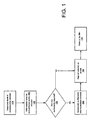
- FIG. 1 illustrates a process flow for fabricating an ABL according to at least one embodiment of the invention.
- the level of desired neutralization is determined (block 110). This may be done by experimentation as differing levels of neutralization may be required depending upon the specific acidic ABL material and specific volatile base being used. The determined level of neutralization will affect device performance, processability and lifetimes. Once determined for a specific OLED device being manufactured, it can of course be held constant. 100% or fully neutralized ABL is the most effective (see below).
- the level of neutralization desired can be achieved by calculating, measuring or experimentally determining how many equivalents of H+ are present in the acidic ABL material. This is well-known in the field of chemistry and will not be discussed in-depth.
- the same number of equivalents of a volatile base is then added to the solution of the conventional acidic ABL material (block 120).
- surfactants or other additives which are required or desired (checked at block 125). If so, then the surfactants or other additives are incorporated into the solution (block 130).
- the neutralized solution is then deposited onto the anode (of an OLED device) (block 160). There are many suitable deposition techniques, some selective and non-selective. Spin-coating is one common technique that can be used in depositing the neutralized ABL solution. Once the solution is deposited, it begins to dry into a film and can be baked in order to harden and stabilize it (block 170). In some embodiments of the invention, the neutralized ABL solution is not baked but merely dried under room temperature in vacuum conditions. Where baking is employed, the bake temperature can be any suitable temperature (for instance 200 degrees C or greater) and any suitable time period which would give the desired result.
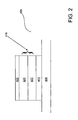
- FIG. 2 shows a cross-sectional view of an embodiment of an OLED device 405 according to at least one embodiment of the invention.
- the OLED device 405 may represent one OLED pixel or sub-pixel of a larger OLED display.
- OLED device 405 is a passive-matrix device since it does not contain its own switching mechanism as with active matrix devices.
- the OLED device 405 includes a first electrode 411 on a substrate 408.
- the term "on” includes when layers are in physical contact or when layers are separated by one or more intervening layers.
- the first electrode 411 may be patterned for pixilated applications or unpatterned for backlight or lighting applications.
- One or more organic materials are deposited above first electrode 411 to form one or more organic layers of an organic stack 416.
- the organic stack 416 is on the first electrode 411.
- the organic stack 416 includes an anode buffer layer ("ABL") 417 and light emitting polymer (LEP) layer 420.
- ABL anode buffer layer
- LEP light emitting polymer
- the OLED device 405 also includes a second electrode 423 on the organic stack 416.
- Other layers than that shown in FIG. 2 may also be added including barrier, charge transport, charge injection, planarizing, diffracting, and interface layers between or among any of the existing layers as desired. Some of these layers, in accordance with the invention, are described in greater detail below.
- the substrate 408 can be any material that can support the organic and metallic layers on it.
- the substrate 408 can be transparent or opaque (e.g., the opaque substrate is used in top-emitting devices). By modifying or filtering the wavelength of light which can pass through the substrate 408, the color of light emitted by the device can be changed.
- the substrate 408 can be comprised of glass, quartz, silicon, plastic, or stainless steel; preferably, the substrate 408 is comprised of thin, flexible glass. The preferred thickness of the substrate 408 depends on the material used and on the application of the device.
- the substrate 408 can be in the form of a sheet or continuous film. The continuous film can be used, for example, for roll-to-roll manufacturing processes which are particularly suited for plastic, metal, and metallized plastic foils.
- a single substrate 408 is typically used to construct a larger OLED display containing many pixels such as OLED device 405 which are then arranged in some pattern.
- the first electrode 411 functions as an anode (the anode is a conductive layer which serves as a hole-injecting layer and which comprises a material with work function greater than about 4.5 eV).
- Typical anode materials include metals (such as platinum, gold, palladium, indium, and the like); metal oxides (such as lead oxide, tin oxide, ITO (Indium Tin Oxide), and the like); graphite; doped inorganic semiconductors (such as silicon, germanium, gallium arsenide, and the like); and doped conducting polymers (such as polyaniline, polypyrrole, polythiophene, and the like).
- the first electrode 411 can be transparent, semi-transparent, or opaque to the wavelength of light generated within the device 405 depending on whether the device 405 is top-emitting or bottom-emitting.
- the thickness of the first electrode 411 can be from about 10 nm to about 1000 nm, preferably, from about 50 nm to about 200 nm, and more preferably, is about 100 nm.
- the first electrode layer 411 can typically be fabricated using any of the techniques known in the art for deposition of thin films, including, for example, vacuum evaporation, sputtering, electron beam deposition, or chemical vapor deposition.
- the ABL 417 typically has a much higher hole mobility than electron mobility and is used to effectively transport holes from the first electrode 411 to the LEP layer 420.
- the ABL 417 can be made of polymers or small molecule materials.
- the ABL 417 is formed from a solution comprising primarily an acidic ABL material and a volatile base wherein the volatile base neutralizes all of the acidic groups in the acidic ABL material, wherein said volatile base comprises at least one of monoalkylamines (NH 2 R), dialkylamines (NHR 2 ), trialkylamines (NR 3 ) such as trimethylamine, triethylamine, and alkylarylamines.
- the acidic ABL material is PEDOT:PSS.
- the volatile base is NH 3 .
- the expectation is that upon baking/drying the ammonia would entirely dissipate leaving the acidic groups again. Unexpectedly, this was found not to be the case.
- the ammonia salts of the PSS in neutralized PEDOT:PSS for instance largely remained even after baking.
- Acidic ABL materials can comprise blends of a conducting polymer such as PEDOT, poly(3,4-dimethoxythiophene), poly(3-methoxythiophene), poly(isothianaphthene) and its derivatives, poly(pyrrole) and its derivatives, PANI and its derivatives, with an acid or polyacid such as poly(styrene sulfonic acid) (PSS), poly(2-acrylamido-2-methyl-l-propanesulfonic acid), sulfonated perfluorinated resins (such as NAFIONTM from DuPont Chemical Corp.), 2-acrylamido-2-methyl-1-propanesulfonic acid, camphorsulfonic acid, dodecylbenzenesulfonic acid, poly(acrylic) acid, and combinations thereof.
- a conducting polymer such as PEDOT, poly(3,4-dimethoxythiophene), poly(3-methoxythiophene), poly(isothianaph
- Volatile bases that are utilized in the invention include, monoalkylamines (NH 2 R), dialkylamines (NHR 2 ), trialkylamines (NR 3 ) such as trimethylamine, triethylamine, and so on, and alkylarylamines. Not claimed but described are ammonia (NH 3 ), arylamines and aromatic heterocycles such as pyridines, pyrroles, imidazoles and triazoles.
- Ionic or non-ionic surfactants can also be added to the solution to improve its processability.
- the solution can be deposited (e.g. by spin coating) onto first electrode 411.
- the deposited solution dries into a film.
- the deposited solution can be baked at a high temperature until hardened sufficiently or simply allowed to vacuum dry at room temperatures.
- PEDOT:PSS material that is neutralized with 30 wt % ammonia (NH 3 ) as an aqueous solution. Furthermore described is PEDOT:PSS that was fully neutralized by the 30% ammonia such that all of the H + ions present in the PSS are neutralized.
- the acidic ABL material was only partially neutralized, for instance at 50% or 75% neutralization. The neutralization can effectively bring the pH of the ABL from between about 1.5 to about 8.
- These mixtures are dark blueish-purple and characterized by an absorption maximum at 850 nm and a weak shoulder at 500 nm, which is slightly different from the absorption found in Baytron CH8000 and other PEDOT:PSS materials.
- the neutralized solution used in fabricating ABL 417 can be deposited onto first electrode 411 using selective deposition techniques or non-selective deposition techniques.
- selective deposition techniques include, for example, ink jet printing, flex printing, and screen printing.
- non-selective deposition techniques include, for example, spin coating, dip coating, web coating, and spray coating.
- the ABL 417 can have a thickness from about 5 nm to about 1000 nm, and is conventionally used from about 50 to about 250 nm.
- an ABL layer of about 100 nm is used.
- Neutralized ABL films which are baked at 200 °C are easier to remove with water than non-neutralized films on the same deposition surface. This is believed due to the diminished capability of neutral ABL material to cross-link as efficiently as the acidic ABL material.
- the water absorption rate of fully neutralized ABL films is less than that convention acidic ABL films.
- Corrosion of the underlying anode (first electrode 411) is almost completely suppressed in neutralized ABL films due to the neutrality of the solution.
- the voltage-current characteristics, resistivity and viscosity are nearly the same or sometimes better with neutralized ABL films compared to conventional acidic ABL films, as shown below in the case of Baytron CH8000.
- the lifetime of OLED devices using neutralized ABL films is improved over films using conventional acidic ABL films (also shown in the accompanying FIGs).
- the LEP layer 420 contains at least one organic material that emits light. These organic light emitting materials generally fall into two categories.
- the first category of OLEDs referred to as polymeric light emitting diodes, or PLEDs, utilize polymers as part of LEP layer 420.
- the polymers may be organic or organo-metallic in nature.
- the term organic also includes organo-metallic materials.
- these polymers are dissolved in an organic solvent, such as toluene or xylene, and spun (spin-coated) onto the device, although other deposition methods are possible.
- Devices utilizing polymeric active electronic materials in LEP layer 420 are especially preferred.
- LEP layer 420 may include a light responsive material that changes its electrical properties in response to the absorption of light.
- Light responsive materials are often used in detectors and solar panels that convert light energy to electrical energy.
- the light emitting organic polymers in the LEP layer 420 can be, for example, EL polymers having a conjugated repeating unit, in particular EL polymers in which neighboring repeating units are bonded in a conjugated manner, such as polythiophenes, polyphenylenes, polythiophenevinylenes, or poly-p-phenylenevinylenes or their families, copolymers, derivatives, or mixtures thereof. More specifically, the organic polymers can be, for example: polyfluorenes; poly-p-phenylenevinylenes that emit white, red, blue, yellow, or green light and are 2-, or 2, 5- substituted poly-p-pheneylenevinylenes; polyspiro polymers.
- Preferred organic emissive polymers include Light Emitting Polymers ("LEPs”) that emit green, red, blue, or white light or their families, copolymers, derivatives, or mixtures thereof.
- LEPs Light Emitting Polymers
- Other polymers include polyspirofluorene-like polymers.
- small organic molecules that emit by fluorescence or by phosphorescence can serve as a light emitting material residing in LEP layer 420.
- small-molecule light emitting materials can also be deposited through evaporative, sublimation, or organic vapor phase deposition methods.
- Combinations of PLED materials and smaller organic molecules can also serve as active electronic layer.
- a PLED may be chemically derivatized with a small organic molecule or simply mixed with a small organic molecule to form LEP layer 420.
- LEP layer 420 can include a material capable of charge transport.
- Charge transport materials include polymers or small molecules that can transport charge carriers.
- organic materials such as polythiophene, derivatized polythiophene, oligomeric polythiophene, derivatized oligomeric polythiophene, pentacene, compositions including C60, and compositions including derivatized C60 may be used.
- LEP layer 420 may also include semiconductors, such as silicon or gallium arsenide.
- the LEP layer 420 typically has a thickness of greater than 80 nm and preferably, between 40 and 125 nm.
- All of the organic layers such as ABL 417 and LEP layer 420 can be ink-jet printed by depositing an organic solution or by spin-coating, or other deposition techniques.
- This organic solution may be any "fluid" or deformable mass capable of flowing under pressure and may include solutions, inks, pastes, emulsions, dispersions and so on.
- the liquid may also contain or be supplemented by further substances which affect the viscosity, contact angle, thickening, affinity, drying, dilution and so on of the deposited drops.
- each of the layers 417 and 420 may be cross-linked or otherwise physically or chemically hardened as desired for stability and maintenance of certain surface properties desirable for deposition of subsequent layers.
- second electrode 423 functions as a cathode when an electric potential is applied across the first electrode 411 and second electrode 423.
- first electrode 411 which serves as the anode
- second electrode 423 which serves as the cathode
- photons are released from active electronic layer 420 that pass through first electrode 411 and substrate 408.
- the thickness of second electrode 423 is from about 10 to about 1000 nanometers (nm), more preferably from about 50 to about 500 nm, and most preferably from about 100 to about 300 nm. While many methods are known to those of ordinary skill in the art by which the first electrode material may be deposited, vacuum deposition methods, such as physical vapor deposition (PVD) are preferred. Other layers (not shown) such as a barrier layer and getter layer may also be used to protect the electronic device. Such layers are well-known in the art and are not specifically discussed herein.
- FIG. 3A illustrates current-voltage curves for various described devices.
- Each device used PEDOT:PSS (Baytron CH8000) for the acidic ABL and an aqueous solution of 30% NH4OH with varying levels of neutralization 0% (a "Control" device), 50%, 75% and 100% neutralization levels were tested.
- the ABL was fabricated to have a thickness of about 100 nm in each device and each device used a white-emitting polyfluorene-based LEP with a thickness of 80 nm.
- the substrates were glass (0.7 mm thickness) coated with an anode of ITO (indium tin oxide) (100 to 120 nm).
- ITO indium tin oxide
- the cathode was formed by a composite of LiF and calcium followed by aluminum. The devices were then encapsulated.
- FIG. 3(B) illustrates luminous efficiency for the same four devices as FIG. 3(A) .
- the luminous efficiency as expressed in terms of brightness (candela/meter 2 ) versus voltage shows that devices with a higher neutralization level show better efficiency and that any neutralization even 50% neutralization, yields a more efficient device than the convention control device which has no neutralization.
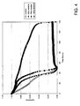
- FIG. 4 illustrates normalized lifetime data for each of the four above-mentioned devices. It can be seen that the lifetime of the devices made with compositions having greater neutralization level ABL is better when compared to the same devices made with compositions having a lower neutralization level ABL. There is less of an initial luminance drop with neutralized ABL devices, and with 100% neutralized devices, the drop in luminance over time is more linear.
- FIG. 5 illustrates voltage driving requirements for each of the four above-mentioned devices when driven under DC conditions.
- the fully neutralized device requires a lower driving voltage and, again, a more linear change in required voltage over time than compared to the control device and partially neutralized devices.
- FIGs 6A and 6B compare water absorption rates for ABL films using conventional ABL material versus those using fully neutralized ABL material under different baking conditions.
- the water absorption rate of thick films of Baytron CH8000 was measured at 22 °C and 34% relative humidity.
- a set of films was vacuum dried at 20 °C, while another was vacuum baked at 200 °C.
- the resulting water absorption is shown in FIG. 6A .
- both the vacuum dried and baked films of non-neutralized conventional Baytron CH8000 showed a weight increase of about 15-16%.
- films fabricated from the same Baytron CH8000 that was then neutralized fully with ammonia showed only a 7-9% weight increase after 90 minutes in the vacuum drying and 200 °C baking cases.
- FIG. 7 illustrates the corrosive effect upon ITO for ABL films using conventional ABL material versus those using fully neutralized ABL material.
- the neutrality of the fully neutralized ABL films suppresses the corrosive effects of the ABL upon anode materials like ITO, as shown in FIG. 7 .
- Conventional ABL (Baytron) eventually corroded the ITO completely within 160-165 hours. With fully neutralized ABL there was hardly if any corrosion of the ITO anode.
- the process of neutralizing the ABL in accordance with the invention may thus have beneficial impacts on processing of films for OLEDs such as corrosion of inkjet print heads.
- OLED display/device described earlier can be used within displays in applications such as, for example, computer displays, information displays in vehicles, television monitors, telephones, printers, area and general lighting, backlighting and illuminated signs.
Landscapes
- Physics & Mathematics (AREA)
- Optics & Photonics (AREA)
- Chemical & Material Sciences (AREA)
- Engineering & Computer Science (AREA)
- Materials Engineering (AREA)
- Electroluminescent Light Sources (AREA)
- Laminated Bodies (AREA)
Claims (10)
- Organisches lichtemittierendes Bauelement (405), umfassend:eine Anode (411);eine Anodenpufferschicht (Anode Buffer Layer, ABL) (417), die auf der Anode (411) angeordnet ist, wobei die Anodenpufferschicht (417) ein saures ABL-Material und eine flüchtige Base enthält, wobei die sauren Gruppen in dem sauren ABL-Material vollständig durch die flüchtige Base neutralisiert sind; undeine lichtemittierende Schicht (420), die auf der Anodenpufferschicht angeordnet ist, wobei die lichtemittierende Schicht (420) dazu in der Lage ist, nach Elektron-Loch-Rekombination darin Licht zu emittieren, wobei die flüchtige Base Monoalkylamine (NH2R), Dialkylamine (NHR2), Trialkylamine (NR3), wie Trimethylamin und Triethylamin, und/oder Alkylarylamine umfasst.
- Organisches lichtemittierendes Bauteil (405) nach Anspruch 1, ferner umfassend:eine Kathode (423), die auf der lichtemittierenden Schicht (420) angeordnet ist.
- Organisches lichtemittierendes Bauteil (405) nach Anspruch 1 oder 2, ferner umfassend:ein Substrat (408), wobei die Anode (411) auf dem Substrat (408) angeordnet ist.
- Organisches lichtemittierendes Bauteil (405) nach einem der Ansprüche 1 bis 3, wobei es sich bei der lichtemittierenden Schicht (420) um ein konjugiertes Polymer handelt.
- Organisches lichtemittierendes Bauteil (405) nach einem der Ansprüche 1 bis 4, wobei die sauren Gruppen zumindest eins aus Poly(styrolsulfonsäure), Poly(2-acrylamido-2-methyl-1-propansulfonsäure), Poly(acrylsäure), ein sulfoniertes perfluoriertes Harz und/oder Salze der Polysäuren umfassen.
- Organisches lichtemittierendes Bauteil (405) nach einem der Ansprüche 1 bis 5, wobei es sich bei dem sauren ABL-Material um PEDOT:PSS handelt.
- Verfahren zur Herstellung einer Anodenpufferschicht (417) für ein organisches lichtemittierendes Bauteil (405), wobei das Verfahren umfasst:Bilden einer Lösung von saurem ABL-Material in einer flüchtigen Base derart, dass die sauren Gruppen in dem sauren ABL-Material vollständig durch die flüchtige Base neutralisiert sind; undAufbringen der Lösung auf eine Anode des organischen lichtemittierenden Bauteils (405), wobei die flüchtige Base Monoalkylamine (NH2R), Dialkylamine (NHR2), Trialkylamine (NR3), wie Trimethylamin und Triethylamin, und/oder Alkylarylamine umfasst.
- Verfahren nach Anspruch 7, das ferner Folgendes umfasst:Brennen des Bauteils mit der aufgebrachten Lösung.
- Verfahren nach Anspruch 8, bei dem die Brenntemperatur mehr als 50°C beträgt.
- Verfahren nach einem der Ansprüche 7 bis 9, das ferner Folgendes umfasst:Trocknen des Bauteils mit der aufgebrachten Lösung.
Applications Claiming Priority (2)
| Application Number | Priority Date | Filing Date | Title |
|---|---|---|---|
| US11/242,180 US20070077451A1 (en) | 2005-09-30 | 2005-09-30 | Neutralized anode buffer layers to improve processing and performances of organic electronic devices |
| PCT/EP2006/007978 WO2007039014A1 (en) | 2005-09-30 | 2006-08-11 | Neutralized anode buffer layers to improve processing and performances of organic electronic devices |
Publications (2)
| Publication Number | Publication Date |
|---|---|
| EP1929560A1 EP1929560A1 (de) | 2008-06-11 |
| EP1929560B1 true EP1929560B1 (de) | 2016-01-06 |
Family
ID=37507844
Family Applications (1)
| Application Number | Title | Priority Date | Filing Date |
|---|---|---|---|
| EP06776795.4A Active EP1929560B1 (de) | 2005-09-30 | 2006-08-11 | Neutralisierte anodenpufferschicht zur verbesserung der verarbeitung und leistungsfähigkeiten organischer lichtemittierender bauelemente und deren herstellungsmethode |
Country Status (7)
| Country | Link |
|---|---|
| US (1) | US20070077451A1 (de) |
| EP (1) | EP1929560B1 (de) |
| JP (1) | JP2009510745A (de) |
| KR (1) | KR101366655B1 (de) |
| CN (1) | CN101278420B (de) |
| TW (1) | TWI321859B (de) |
| WO (1) | WO2007039014A1 (de) |
Families Citing this family (12)
| Publication number | Priority date | Publication date | Assignee | Title |
|---|---|---|---|---|
| US7736540B1 (en) * | 2004-12-30 | 2010-06-15 | E. I. Du Pont De Nemours And Company | Organic compositions for depositing onto fluorinated surfaces |
| EP2336255A1 (de) * | 2009-12-17 | 2011-06-22 | Basf Se | Organische Elektronikmaterialien mit verbesserter Stabilität und Leistung |
| WO2012061399A1 (en) | 2010-11-03 | 2012-05-10 | Cambrios Technologies Corporation | Coating compositions for forming nanocomposite films |
| CN102881838B (zh) * | 2012-09-28 | 2016-08-10 | 京东方科技集团股份有限公司 | 发光器件的封装结构及封装方法、显示装置 |
| JP6182884B2 (ja) * | 2013-02-05 | 2017-08-23 | 日産化学工業株式会社 | 電荷輸送性ワニス |
| DE102013005152A1 (de) | 2013-03-26 | 2014-10-02 | Heraeus Precious Metals Gmbh & Co. Kg | VERFAHREN ZUR HERSTELLUNG VON HOCHVlSKOSEN UND LAGERUNGSSTABlLEN DlSPERSlONEN ZUR HERSTELLUNG ELEKTRlSCH LElTENDER SCHlCHTEN |
| KR101679711B1 (ko) | 2014-06-13 | 2016-11-25 | 주식회사 엘지화학 | 중성화된 전도성 수분산액 조성물 및 그 제조방법 |
| CN104240798A (zh) * | 2014-09-25 | 2014-12-24 | 上海交通大学 | 一种透明导电薄膜及其制备方法 |
| EP3325563A4 (de) * | 2015-07-17 | 2019-03-27 | Nissan Chemical Corporation | Nichtwässrige tintenzusammensetzungen mit metalloiden nanopartikeln zur verwendung in der organischen elektronik |
| JP6547792B2 (ja) * | 2017-06-12 | 2019-07-24 | 日産化学株式会社 | 電荷輸送性ワニス |
| JP2017208552A (ja) * | 2017-06-12 | 2017-11-24 | 日産化学工業株式会社 | 電荷輸送性ワニス |
| JPWO2022054640A1 (de) * | 2020-09-08 | 2022-03-17 |
Citations (4)
| Publication number | Priority date | Publication date | Assignee | Title |
|---|---|---|---|---|
| EP1505664A2 (de) * | 2003-08-05 | 2005-02-09 | H.C. Starck GmbH | Transparente Elektrode für elektro-optische Aufbauten |
| JP2005108504A (ja) * | 2003-09-29 | 2005-04-21 | Dainippon Printing Co Ltd | 有機エレクトロルミネッセンス素子およびその製造方法 |
| US20050129857A1 (en) * | 2003-12-15 | 2005-06-16 | Steve Pollack | Synthesis of highly conducting and transparent thin polymer films |
| US20050151468A1 (en) * | 2003-11-21 | 2005-07-14 | Park Jin-Woo | Organic electroluminescent device |
Family Cites Families (9)
| Publication number | Priority date | Publication date | Assignee | Title |
|---|---|---|---|---|
| DE69911753T2 (de) * | 1998-03-13 | 2004-08-12 | Cambridge Display Technology Ltd. | Elektrolumineszente anordnungen |
| US6916553B2 (en) * | 2001-03-29 | 2005-07-12 | Agfa-Gevaert | Stable electroluminescent devices |
| US6955772B2 (en) * | 2001-03-29 | 2005-10-18 | Agfa-Gevaert | Aqueous composition containing a polymer or copolymer of a 3,4-dialkoxythiophene and a non-newtonian binder |
| EP1780232A1 (de) * | 2001-12-04 | 2007-05-02 | Agfa-Gevaert | Zusammensetzung enthaltend ein Polymer oder Copolymer von 3,4-Dialkoxythiopen und ein nicht-wässriges Lösungsmittel |
| US7317047B2 (en) * | 2002-09-24 | 2008-01-08 | E.I. Du Pont De Nemours And Company | Electrically conducting organic polymer/nanoparticle composites and methods for use thereof |
| US7390438B2 (en) * | 2003-04-22 | 2008-06-24 | E.I. Du Pont De Nemours And Company | Water dispersible substituted polydioxythiophenes made with fluorinated polymeric sulfonic acid colloids |
| CN1833323A (zh) * | 2003-08-06 | 2006-09-13 | 皇家飞利浦电子股份有限公司 | 发光二极管 |
| TW200531587A (en) * | 2003-12-09 | 2005-09-16 | Showa Denko Kk | Polymer for anode buffer layer, coating solution for anode buffer layer, and organic light emitting device |
| US20060177690A1 (en) * | 2005-02-07 | 2006-08-10 | Osram Opto Semiconductors Gmbh & Co. Ohg | Tri-layer PLED devices with both room-temperature and high-temperature operational stability |
-
2005
- 2005-09-30 US US11/242,180 patent/US20070077451A1/en not_active Abandoned
-
2006
- 2006-08-11 JP JP2008532613A patent/JP2009510745A/ja active Pending
- 2006-08-11 KR KR1020087010500A patent/KR101366655B1/ko not_active IP Right Cessation
- 2006-08-11 WO PCT/EP2006/007978 patent/WO2007039014A1/en active Application Filing
- 2006-08-11 EP EP06776795.4A patent/EP1929560B1/de active Active
- 2006-08-11 CN CN2006800364054A patent/CN101278420B/zh active Active
- 2006-09-25 TW TW095135300A patent/TWI321859B/zh not_active IP Right Cessation
Patent Citations (4)
| Publication number | Priority date | Publication date | Assignee | Title |
|---|---|---|---|---|
| EP1505664A2 (de) * | 2003-08-05 | 2005-02-09 | H.C. Starck GmbH | Transparente Elektrode für elektro-optische Aufbauten |
| JP2005108504A (ja) * | 2003-09-29 | 2005-04-21 | Dainippon Printing Co Ltd | 有機エレクトロルミネッセンス素子およびその製造方法 |
| US20050151468A1 (en) * | 2003-11-21 | 2005-07-14 | Park Jin-Woo | Organic electroluminescent device |
| US20050129857A1 (en) * | 2003-12-15 | 2005-06-16 | Steve Pollack | Synthesis of highly conducting and transparent thin polymer films |
Also Published As
| Publication number | Publication date |
|---|---|
| EP1929560A1 (de) | 2008-06-11 |
| CN101278420A (zh) | 2008-10-01 |
| US20070077451A1 (en) | 2007-04-05 |
| TWI321859B (en) | 2010-03-11 |
| KR101366655B1 (ko) | 2014-02-24 |
| TW200729585A (en) | 2007-08-01 |
| WO2007039014A1 (en) | 2007-04-12 |
| KR20080063807A (ko) | 2008-07-07 |
| JP2009510745A (ja) | 2009-03-12 |
| CN101278420B (zh) | 2010-10-13 |
Similar Documents
| Publication | Publication Date | Title |
|---|---|---|
| EP1929560B1 (de) | Neutralisierte anodenpufferschicht zur verbesserung der verarbeitung und leistungsfähigkeiten organischer lichtemittierender bauelemente und deren herstellungsmethode | |
| EP1753047B1 (de) | In Flüssigphase verarbeitete, vernetzbare Lochinjektion- und Lochtransport-Polymere für OLEDs. | |
| US7132788B2 (en) | Optimal bank shapes for inkjet printing | |
| KR100853897B1 (ko) | 유기 전계 발광 소자 | |
| US20060159842A1 (en) | Printing of organic electronic devices | |
| EP1816690B1 (de) | OLED mit bereichsdefinierter mehrfarbiger Emission innerhalb eines Einzelbeleuchtungselements | |
| US7022534B2 (en) | Optimal bank height for inkjet printing | |
| US7407716B2 (en) | Light emitting devices with multiple light emitting layers to achieve broad spectrum | |
| EP1746669A2 (de) | Eine dicke Schicht aus lichtemittierenden Polymeren zur Verbesserung der Ausbeute und Lebenszeit von OLEDs | |
| US7452613B2 (en) | White organic electroluminescent device | |
| US7550915B2 (en) | Organic electronic device with hole injection | |
| US20050276910A1 (en) | Post processing of films to improve film quality | |
| US20060290272A1 (en) | Enhancement of light extraction using gel layers with excavations | |
| US7358526B2 (en) | OLED separating structures | |
| EP1705729B1 (de) | Hybride Lichtquelle auf Basis von Polymeren und kleinen Molekülen | |
| US7626332B2 (en) | Luminance uniformity enhancement methods for an OLED light source | |
| US20060177690A1 (en) | Tri-layer PLED devices with both room-temperature and high-temperature operational stability | |
| US20060065889A1 (en) | Compositions for making organic thin films used in organic electronic devices | |
| US20050151129A1 (en) | Deposition of conducting polymers | |
| US20060017057A1 (en) | Device structure to improve OLED reliability | |
| WO2005096401A2 (en) | Device structure to improve oled reliability |
Legal Events
| Date | Code | Title | Description |
|---|---|---|---|
| PUAI | Public reference made under article 153(3) epc to a published international application that has entered the european phase |
Free format text: ORIGINAL CODE: 0009012 |
|
| 17P | Request for examination filed |
Effective date: 20080204 |
|
| AK | Designated contracting states |
Kind code of ref document: A1 Designated state(s): DE |
|
| RBV | Designated contracting states (corrected) |
Designated state(s): DE |
|
| 17Q | First examination report despatched |
Effective date: 20091221 |
|
| DAX | Request for extension of the european patent (deleted) | ||
| GRAP | Despatch of communication of intention to grant a patent |
Free format text: ORIGINAL CODE: EPIDOSNIGR1 |
|
| INTG | Intention to grant announced |
Effective date: 20150724 |
|
| RAP1 | Party data changed (applicant data changed or rights of an application transferred) |
Owner name: OSRAM OLED GMBH |
|
| GRAS | Grant fee paid |
Free format text: ORIGINAL CODE: EPIDOSNIGR3 |
|
| GRAA | (expected) grant |
Free format text: ORIGINAL CODE: 0009210 |
|
| AK | Designated contracting states |
Kind code of ref document: B1 Designated state(s): DE |
|
| REG | Reference to a national code |
Ref country code: DE Ref legal event code: R096 Ref document number: 602006047665 Country of ref document: DE |
|
| REG | Reference to a national code |
Ref country code: DE Ref legal event code: R097 Ref document number: 602006047665 Country of ref document: DE |
|
| PLBE | No opposition filed within time limit |
Free format text: ORIGINAL CODE: 0009261 |
|
| STAA | Information on the status of an ep patent application or granted ep patent |
Free format text: STATUS: NO OPPOSITION FILED WITHIN TIME LIMIT |
|
| 26N | No opposition filed |
Effective date: 20161007 |
|
| REG | Reference to a national code |
Ref country code: DE Ref legal event code: R081 Ref document number: 602006047665 Country of ref document: DE Owner name: PICTIVA DISPLAYS INTERNATIONAL LIMITED, IE Free format text: FORMER OWNER: OSRAM OLED GMBH, 93049 REGENSBURG, DE Ref country code: DE Ref legal event code: R082 Ref document number: 602006047665 Country of ref document: DE Representative=s name: EPPING HERMANN FISCHER PATENTANWALTSGESELLSCHA, DE |
|
| REG | Reference to a national code |
Ref country code: DE Ref legal event code: R079 Ref document number: 602006047665 Country of ref document: DE Free format text: PREVIOUS MAIN CLASS: H01L0051540000 Ipc: H10K0085000000 |
|
| PGFP | Annual fee paid to national office [announced via postgrant information from national office to epo] |
Ref country code: DE Payment date: 20230823 Year of fee payment: 18 |