EP1501100B1 - Nichtflüchtige Speicheranordnung, Speichersystem und Betriebsverfahren - Google Patents
Nichtflüchtige Speicheranordnung, Speichersystem und Betriebsverfahren Download PDFInfo
- Publication number
- EP1501100B1 EP1501100B1 EP04016660.5A EP04016660A EP1501100B1 EP 1501100 B1 EP1501100 B1 EP 1501100B1 EP 04016660 A EP04016660 A EP 04016660A EP 1501100 B1 EP1501100 B1 EP 1501100B1
- Authority
- EP
- European Patent Office
- Prior art keywords
- read
- output
- memory device
- flash memory
- signal
- Prior art date
- Legal status (The legal status is an assumption and is not a legal conclusion. Google has not performed a legal analysis and makes no representation as to the accuracy of the status listed.)
- Expired - Lifetime
Links
Images


Classifications
-
- G—PHYSICS
- G11—INFORMATION STORAGE
- G11C—STATIC STORES
- G11C16/00—Erasable programmable read-only memories
- G11C16/02—Erasable programmable read-only memories electrically programmable
- G11C16/06—Auxiliary circuits, e.g. for writing into memory
- G11C16/26—Sensing or reading circuits; Data output circuits
-
- G—PHYSICS
- G11—INFORMATION STORAGE
- G11C—STATIC STORES
- G11C7/00—Arrangements for writing information into, or reading information out from, a digital store
- G11C7/10—Input/output [I/O] data interface arrangements, e.g. I/O data control circuits, I/O data buffers
- G11C7/1015—Read-write modes for single port memories, i.e. having either a random port or a serial port
- G11C7/1018—Serial bit line access mode, e.g. using bit line address shift registers, bit line address counters, bit line burst counters
- G11C7/1021—Page serial bit line access mode, i.e. using an enabled row address stroke pulse with its associated word line address and a sequence of enabled column address stroke pulses each with its associated bit line address
- G11C7/1024—Extended data output [EDO] mode, i.e. keeping output buffer enabled during an extended period of time
Definitions
- the invention relates to a nonvolatile memory device, in particular a flash memory device, a memory system incorporating such a device, and corresponding operating methods.
- Flash memory is a type of nonvolatile rewritable memory useful in a wide variety of digital data applications that require occasional writing and/or rewriting of data, nonvolatile storage, and relatively high-speed read capability.
- some flash memory devices include a "burst-read” or "page-read” operation.
- a flash memory device with this capability responds to a read request by reading a "page” of memory into an on-chip buffer, and then outputting successive data elements from this buffer in response to a group of sequential read pulses.
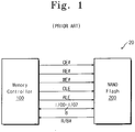
- Figure 1 illustrates a basic flash memory system 20, including a memory controller 100 and a NAND flash memory device 200.
- Memory controller 100 supplies control signals CE#, RE#, WE#, CLE, and ALE to memory device 200.
- Memory controller 100 and memory device 200 also share a bi-directional input/output (I/O) bus, shown in Figure 1 as a group of eight signal lines I/O0 - 1/07.
- Memory device 200 also drives an R/B# signal to memory controller 200.
- I/O input/output
- Memory controller 100 may be a dedicated circuit or integrated into a larger circuit with additional functionality, such as a digital processor.
- Chip enable signal CE# provides selection control: other signals can be routed to multiple memory devices, and the only device that will respond is the one to which memory controller 100 asserts CE#.
- Read enable signal RE# actually causes memory device 200 to drive read data onto the I/O bus when asserted.
- Write enable signal WE# causes memory device 200 to latch address, command, or write data off of the I/O bus on a positive transition.
- Command latch enable signal CLE when asserted, causes data latched at the memory device's I/O port to be interpreted as a command.
- address latch enable signal ALE when asserted, causes data latched at the memory device's I/O port to be interpreted as address data.
- I/O0 - I/O7 are driven by memory controller 100 to transfer commands, address, and write data to memory device 200.
- I/O0 - I/O7 are driven by memory device 200 to transfer read data to memory controller 100.
- memory controller 100 and flash memory device 200 are not driving the I/O bus, they each place their respective drivers in a high-impedance (high-z) state.
- flash memory device 200 has the capability to drive ready/busy signal R/B# to memory controller 100. Memory device 200 pulls this signal low when it is programming, erasing, or reading from the memory array.
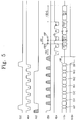
- Figure 2 contains a timing diagram for the data transfer portion of a data read operation for system 20.
- memory controller 100 commands memory device 200 to read data for a specific page of its memory. Flash memory device 200 pulls R/B# low while the specific page is accessed from the memory array to indicate that it is busy.
- R/B# returns to a high state
- memory controller 100 is permitted to take RE# low (while CE# is low) to cause memory device 200 to drive a first data element Dout N onto the I/O bus.
- Memory controller 100 then takes RE# high as it latches Dout N off of the I/O bus.
- Memory device 200 then returns the I/O bus to a high-z state and awaits a new read cycle.
- Timing parameter tREA represents the worst-case read-enable-to-access time, i.e., the delay between when memory controller 100 takes RE# low and when memory device 200 begins to drive Dout N onto the I/O bus.
- Timing parameter tRC represents the shortest read cycle time, i.e., time between successive reads in a burst, that can be supported by the device.
- Parameter tRC generally has two sub-parameters tRP and tREH as shown.
- Timing parameter tRP represents the minimum read pulse width, i.e., time between RE# assertion and data latching.
- timing parameter tREH represents the RE# high hold time, i.e., the minimum time that memory controller 100 must hold RE# high between successive read pulses.
- memory controllers can support a higher bus operating speed than supported by a NAND flash memory, particularly for low-voltage flash memory.
- a NAND flash memory with a reduced read cycle time would therefore be advantageous in speeding overall system performance.
- the pulse width, tRP cannot be reduced below the access time tREA or else the memory controller will latch erroneous data before the memory device has driven the requested data to the memory controller.
- US 6,222,767 B1 discloses a non-volatile memory device according to the preamble of claim 1.
- a flash memory device operating method is disclosed in Jin-Ki Kim et al., A 120-mm2 64-Mb NAND Flash Memory Achieving 180 ns/Byte Effective Program Speed, IEEE Journal of Solid-State Circuits, Vol. 32, No. 5, May 1997, page 670 .
- US 5,357,530 discloses a data output control circuit of a semiconductor memory device, said circuit comprising a plurality of circuit blocks each including a data output buffer controlled by an output enable signal generated by an address transition detecting circuit including an input buffer, an input signal detector, a controller, and a data output controller in series.
- the invention solves this problem by providing for a nonvolatile flash memory device having the features of claim 1, a memory system having the features of claim 11, a flash memory device operating method having the features of claim 16, and a memory system operating method having the features of claim 19.
- a nonvolatile flash memory device having the features of claim 1
- a memory system having the features of claim 11
- a flash memory device operating method having the features of claim 16
- a memory system operating method having the features of claim 19.
- the invention includes nonvolatile flash memory device embodiments, operating method embodiments, and memory system embodiments that implement what is referred to as a pipelined burst read.
- the memory controller requires two read enable assertions to read a memory cell. The first assertion causes the flash memory to drive a requested data word (where a word is defined according to the bus width) onto the data bus. The memory controller does not, however, latch the requested data word until it asserts read enable a second time. When the flash memory receives the second read enable, it is permitted to begin driving a next requested data word onto the data bus.
- tREA read-enable-to-access time
- some embodiments can support both non-pipelined and pipelined read operations, as instructed by the memory controller, using the same signal lines.
- Figure 3 illustrates a basic pipelined burst read as implemented in some embodiments of the invention.
- the memory device allows R/B# to return to a high state.
- the memory controller is then allowed to drive RE# low, causing the memory device to drive Dout N onto the I/O bus after a tREA access time.
- the memory controller does not expect Dout N to be valid after a read pulse tRP time (when RE# is driven high). Instead, the memory controller latches Dout N as it asserts RE# for a second time, i.e., tRC after the first assertion of RE#.
- the flash memory device When the flash memory device receives the second assertion of RE#, it begins a second access cycle, this time for Dout N +1.
- the memory device output drivers In the expected pipelined operating mode, the memory device output drivers never enter a high-z state during the burst operation, but transition directly from one data word to the next data word on successive RE# assertions. Thus Dout N +1 is not latched to the memory controller until a third assertion of RE#. This pattern continues for each successive data word read.
- the memory controller can handle this condition by either: a) ensuring that it latches Dout M , without transmitting an additional RE# pulse, after tRC seconds from the last RE# assertion but prior to tREHS seconds after the last RE# deassertion; or b) issuing an additional RE# pulse to latch Dout M, and then ignoring Dout M +1 that will be placed on the data bus due to the additional RE# pulse.
- Flash memory device 200-1 includes a flash memory array 210, address buffer and latch 220, column decoder 230, row decoder 240, data register and sense amplifier 250, I/O buffer and latch 260, global buffer 280, control circuit 300, and output driver 400.
- control circuit 300 and output driver 400 are modified, however, to provide a pipelined burst read operation. In some embodiments, other blocks are also modified to provide pipelined burst read operation features.
- the specific blocks affected by various embodiments of the invention will be described in detail, along with description of the unaffected blocks as necessary for a full understanding of the present invention. It is expected that those skilled in the art are familiar with the general operation of, for instance, flash memory cells, blocks, column and row decoders, sense amplifiers, etc., and an understanding of the detailed operation of these elements is not critical to the present invention.
- Control circuit 300 latches the value present on the I/O port into global buffer 280 on a low-to-high WE# transition when CE# is low. Thus at the trailing edge of write pulse 1, a value 00h (where h indicates hexadecimal notation) is latched into global buffer 280. Also, because CLE is asserted high when this data is latched, the data is interpreted as a command and transferred from global buffer 280 to command register 290.
- write enable pulse 7 is used in conjunction with a second assertion of CLE to transfer a read command 30h to command register 290.
- memory device 200-1 pulls R/B# low to indicate that it is busy, and then initiates a page read from flash memory array 210 using the supplied row address RA and column address CA.
- the requested page is transferred to I/O buffer and latch 260, and a word pointer in I/O buffer and latch 260 is set to the first requested address.
- the requested data is ready to be transferred to the memory controller. Accordingly, R/B# is allowed to return to a high value.
- Control circuit 300 interprets the falling edge of read-enable pulse n as a request to drive the currently pointed-to data word (Dout N, appearing on an internal Data Out bus) in I/O buffer and latch 260 onto the I/O bus.
- Control circuit responds by asserting a pipelined output enable signal POE to output driver 400.
- Output driver 400 responds by driving the value Dout N from the Data Out bus onto the I/O bus, with the data appearing tREA seconds after assertion n of RE#.
- tREA is shown as greater than tRP, but this is not strictly necessary because data will not be read for at least tRC seconds after assertion n of RE#. Parameter tREA must, however, be less than tRC to ensure proper operation.
- the memory controller can drive RE# low again provided at least tRC seconds have passed since the falling edge of read enable pulse n.
- the memory controller initiates a read-enable pulse n +1 while latching data Dout N from the I/O bus.
- Control circuit 300 detects the falling edge of read-enable pulse n +1, and signals I/O buffer and latch 260 to increment its internal pointer to Dout N +1 and place Dout N +1 on the Data Out bus. Internal pipelined output enable signal remains asserted during this operation, such that output driver 400 transitions to driving Dout N +1 without ever entering a high-z state.
- the memory controller can drive a new read enable pulse n+2 to the memory device.
- the memory controller can latch data Dout N +1 from the I/O bus while initiating read enable pulse n +2.
- the pipelined burst read operation can continue in this manner until the memory controller has received the last data value that it needs (either Dout M or Dout M +1).
- the following description illustrates at least one method for ending the pipelined burst read operation.
- the memory controller latches Dout M from the I/O bus.
- the memory device interprets the m +1 th read-enable pulse as a request, intended or not, for it to drive Dout M +1 onto the I/O bus.
- the memory device thus drives Dout M +1 onto the I/O bus and awaits an m +2 th read-enable pulse that is not forthcoming.
- the memory controller can choose to ignore Dout M +1, or to latch Dout M +1 if it can do so during the data valid period without initiating an m +2 th read-enable pulse. Meanwhile, control circuit 300 has detected the rising edge of the m +1 th read-enable pulse and is marking the passage of time. Once a time period tREHS passes without an m +2 th read-enable pulse falling edge being detected, control circuit 300 deasserts POE, causing output driver 400 to enter a high-z state. The memory controller need only hold RE# high for tREHS seconds to ensure that the memory device has released the I/O bus, and then the memory controller can initiate a new command.
- FIG. 6 illustrates the portion of the circuitry, within control circuit 300, that is used to generate the POE output enable signal to output driver 400 in some embodiments of the present invention.
- control circuit 300 comprised an nRE buffer 310 to generate an internal read enable signal IRE based on CE# and RE#, a judge circuit 320 that receives IRE as its input, a 2:1 multiplexer 330 to select one of IRE and the output of judge circuit 320 based on a mux select signal EDO_EN, and a Dout (Data out) control circuit 340 to create output enable signal POE based, at least in part, on the output of multiplexer 330.
- nRE buffer 310 to generate an internal read enable signal IRE based on CE# and RE#
- a judge circuit 320 that receives IRE as its input
- a 2:1 multiplexer 330 to select one of IRE and the output of judge circuit 320 based on a mux select signal EDO_EN
- a Dout (Data out) control circuit 340
- Figure 7 shows one embodiment of nRE buffer 310, comprising a two-input NOR gate G1, an inverter I1.
- the external signals CE# and RE# are coupled, respectively, to the two inputs of NOR gate G1.
- the output of NOR gate G1 is supplied to the input of inverter I1, and the output of inverter I1 is supplied as internal read enable signal IRE.
- IRE is asserted low whenever both CE# and RE# are asserted low. Assuming that CE# is held low by the memory controller for the duration of an RE# pulse, IRE will mirror RE#.
- Figure 8 shows one embodiment of judge circuit 320, comprising a delay element 322 and a two-input NAND gate G2.
- Internal read enable signal IRE is supplied as an input to delay element 322 and as one input to NAND gate G2.
- the output of delay element 322, shown as signal "B,” is supplied as the second input to NAND gate G2.
- NAND gate G2 generates a signal DOUT_FLAG.
- DOUT_FLAG remains asserted high as long as at least one of IRE and B is low. Assuming that IRE has been high for longer than the delay period, this circuit responds to IRE going low by driving DOUT_FLAG high. Assuming that the delay of element 322 is shorter than the low pulse on IRE, signal B will go low before IRE returns to high, thus holding DOUT_FLAG high. If IRE is again pulsed low before signal B follows IRE high, DOUT_FLAG remains high. Under these conditions, DOUT_FLAG will stay high indefinitely as long as IRE continues to toggle, and will only return to a low value if signal IRE returns high and stays high for longer than the delay period of element 322.
- judge circuit 322 should enable the data output upon receiving a first read enable pulse, and continue to enable the data output as long as the read enable signal continue to toggle at least once in a period tREHS.
- the judge circuit changes its state to low.
- the length of period tREHS is a design parameter that can be set to provide correct operation in a desired range of read cycle times.
- Figure 9 illustrates one embodiment of multiplexer 330, including inverters 12 and 13 and transmission gates TG1 and TG2.
- 12 inverts input signal IRE and supplies the inverted signal to the input of transmission gate TG1.
- Input signal DOUT_FLAG is supplied to the input of transmission gate TG2.
- the outputs of transmission gates TG1 and TG2 are tied together at an output A.
- EDO_EN inverts the control signal EDO_EN.
- EDO_EN and the inverter 13 output are supplied to the control gates of TG1 such that TG1 passes its input to output A when EDO_EN is low.
- EDO_EN and the inverter 13 output are supplied in complementary fashion to the control gates of TG2 such that TG2 passes its input to output A when EDO_EN is high. Accordingly, EDO_EN selects either IRE (inverted) or DOUT_FLAG as output A.
- EDO_EN can be used advantageously to switch between two burst read operating modes. When EDO_EN is low, burst read operations similar to the prior art are performed. When EDO_EN is high, pipelined burst read operations are performed.
- command register 290 contains a command decoder 292, an EDO_EN mode register 294, and a power-up detector 296.
- Power-up detector 296 generates a POR signal during the power-up period. The POR signal sets EDO_EN mode register 294 to a logic low state (or, if desired in a particular application, a logic high state), such that the device is in a determinate burst read mode state.
- command decoder 292 sets EDO_EN mode register 294 to a logic low state. Also, if command decoder 292 receives a command signal CMD indicating that the memory controller desires to use a second burst read operation type, command decoder 292 sets EDO_EN mode register 294 to a logic high state.
- the command signal CMD can be a dedicated mode-setting command.
- EDO_EN mode register 294 when the memory controller issues the first read command type, EDO_EN mode register 294 is set to a logic low state, and when the memory controller issues the second read command type EDO_EN mode register 294 is set to a logic high state.
- FIG 11 illustrates one embodiment of Dout control circuit 340 shown in Figure 6 .
- Dout control circuit 340 consists of two serial inverters 14 and 15, which merely buffer output A from multiplexer 330 to provide output enable signal POE.
- output enable POE is high when both CE# and RE# are low, and low otherwise.
- the output driver is thus controlled according to Figure 2 , having a DATA state when RE# is low (and the chip is selected) and a high-z state otherwise.
- multiplexer 330 selects DOUT_FLAG, output enable POE transitions to high when both CE# and RE# are low, placing the output driver in a DATA state.
- POE persists in a high state as long as RE# toggles (while the chip is selected) within a time tREHS. POE continues to persist in a high state for tREHS seconds after the last positive transition of RE#, and then reverts to a low state (placing the output driver in a high-z state).
- Bit lane i output driver comprises a two-input NAND gate G3, an inverter 16, a two-input NOR gate G4, a p-channel drive transistor M2, and an n-channel driver transistor M3.
- Data out bit lane value Dout i from I/O buffer and latch 260 is supplied to one input of gates G3 and G4.
- Output enable POE from control circuit 300 is supplied to the other input of NAND gate G3, and to the input of inverter 16.
- the output of inverter 16 is supplied as the second input to NOR gate G4.
- NAND gate G3 drives the gate of p-channel drive transistor M2, and the output of NOR gate G4 drives the gate of n-channel drive transistor M3.
- P-channel drive transistor M2 has its source connected to V CC and its drain connected to input/output bus line I/O i .
- N-channel drive transistor M3 has its source connected to V SS and its drain connected to input/output bus line I/O i . Accordingly, when M2 is on I/O i is pulled high, when M3 is on I/O is pulled low, and when M2 and M3 are both off the output driver is in a high-z state.
- the output driver circuit operates as follows. When POE is low, NAND gate G3 has a high output no matter what the state of Dout i , and thus p-channel drive transistor M2 is off. Also when POE is low, NOR gate G4 has a low output no matter what the state of Dout i , and thus n-channel drive transistor M3 is also off, and the output driver is in a high-z state.
- Dout control 340 shown in Figure 6 can use other state information to control POE in addition to multiplexer 330 output A.
- Figure 13 illustrates such an embodiment, comprising a three-input OR gate G5, a three-input NOR gate G6, two two-input NAND gates G7 and G8, and two inverters 17 and 18.
- a read control circuit 450 indicates that data is available by asserting a signal SENSE_END.
- the memory controller can issue a 70h command to request state information, e.g., did the last program or erase function complete normally. Since this data does not have to be read from the memory array, command register 290 can assert a 70h flag to indicate that the state information is ready to be driven on the I/O bus.
- the memory controller can also issue a 90h command to request device ID information such as a maker code, device code, chip number, cell type, page size and spare size, and data organization. Since this data does not have to be read from the memory array, command register 290 can assert a 90h flag to indicate that the ID information is ready to be driven on the I/O bus.
- OR gate G5 ors the 70h flag, 90h flag, and SENSE_END signals.
- Dout control 340 of Figure 13 also contains circuitry to disable POE when the memory controller is attempting to drive data on the I/O bus.
- NOR gate G6 ors internal address latch enable signal IALE, internal command latch enable signal ICLE, and internal write enable signal IWE, and supplies its output to one input of NAND gate G7 with serial inverter 17.
- Multiplexer 330 output signal A is supplied to the other input of NAND gate G7. Accordingly, POE is disabled when the memory controller is attempting to drive data on the I/O bus.
Landscapes
- Read Only Memory (AREA)
Claims (21)
- Nicht-flüchtiges Flash-Speicherbauelement mit- einem Ausgabepuffer (260), der dafür eingerichtet ist, ein Datenausgabesignal in Reaktion auf eine Bestätigung eines Lesefreigabesignals bereitzustellen, und- einem Dreizustands-Ausgabetreiber (400), der an das Datenausgabesignal und ein Ausgabefreigabesignal gekoppelt und dafür eingerichtet ist, das Datenausgabesignal auf einem Ausgabeknoten zu treiben, wenn das Ausgabefreigabesignal bestätigt wird, wobei der Dreizustands-Ausgabetreiber ansonsten eine hohe Impedanz am Ausgangsknoten aufweist, gekennzeichnet durch- einen Beurteilungsschaltkreis (320), um ein Ausgabemarkierungssignal in Reaktion auf die Bestätigung des Lesefreigabesignals zu bestätigen und die Bestätigung des Ausgabemarkierungssignals aufzuheben, wenn die Bestätigung des Lesefreigabesignals mindestens für eine Haltezeit aufgehoben bleibt, wobei in wenigstens einem Lesemodus das Ausgabefreigabesignal auf das Ausgabemarkierungssignal reagiert, und- einen Multiplexer (330) mit einer Multiplexerausgabe, die basierend auf einem Lesemoduseingabesignal aus einer ersten und einer zweiten Signaleingabe auswählbar ist, wobei die erste Signalausgabe mit dem Ausgabemarkierungssignal gekoppelt ist, die zweite Signaleingabe mit dem Lesefreigabesignal gekoppelt ist und das Ausgabefreigabesignal auf die Multiplexerausgabe anspricht.
- Nicht-flüchtiges Flash-Speicherbauelement nach Anspruch 1, wobei der Multiplexer Folgendes aufweist:- ein erstes Übertragungsgatter mit einem mit der ersten Signaleingabe verbundenen Eingang, einem mit der Multiplexerausgabe verbundenen Ausgang und einem Steuergate, das zum Einschalten des ersten Übertragungsgatters, wenn sich das Lesemoduseingabesignal in einem ersten Logikzustand befindet, verschaltet ist, und- ein zweites Übertragungsgatter mit einem mit der zweiten Signaleingabe verbundenen Eingang, einem mit der Multiplexerausgabe verbundenen Ausgang und einem Steuergate, das zum Einschalten des zweiten Übertragungsgatters, wenn sich das Lesemoduseingabesignal in einem zweiten Logikzustand befindet, verschaltet ist.
- Nicht-flüchtiges Flash-Speicherbauelement nach Anspruch 1 oder 2, das des Weiteren ein programmierbares Modusregister zur Erzeugung des Lesemoduseingabesignals aufweist.
- Nicht-flüchtiges Flash-Speicherbauelement nach Anspruch 3, wobei das programmierbare Modusregister in Reaktion auf einen von dem Bauelement während des Betriebs empfangenen Modusregisterbefehl programmierbar ist und eine Rücksetzlogik zum Setzen des Registerstatus beim Anschalten des Bauelements besitzt.
- Nicht-flüchtiges Flash-Speicherbauelement nach einem der Ansprüche 1 bis 4, das des Weiteren einen Datenausgabesteuerschaltkreis zum Empfangen der Multiplexerausgabe und Erzeugen des Ausgabefreigabesignals aufweist.
- Nicht-flüchtiges Flash-Speicherbauelement nach Anspruch 5, das zur Durchführung von Registerlesevorgängen und Datenarraylesevorgängen befähigt ist, wobei es der Datenausgabeschaltkreis dem Ausgabefreigabesignal ermöglicht, auf die Multiplexerausgabe sowohl dann, wenn ein Registerlesevorgang angefordert wird, als auch dann zu reagieren, wenn ein Arraylesevorgang angefordert wird und Arraydaten zur Ausgabe als das Datenausgabesignal bereitstehen.
- Nicht-flüchtiges Flash-Speicherbauelement nach einem der Ansprüche 1 bis 6, das des Weiteren einen Lesefreigabepuffer zum Bestätigen des Lesefreigabesignals aufweist, wenn sowohl ein externes Chipfreigabesignal als auch ein externes Lesefreigabesignal bestätigt werden.
- Nicht-flüchtiges Flash-Speicherbauelement nach einem der Ansprüche 1 bis 5, das des Weiteren Folgendes aufweist:- einen programmierbaren Modusschaltkreis (290) zur Erzeugung eines Lesemoduseingabesignals, das zum Anzeigen von wenigstens zwei Lesemodi befähigt ist, einschließlich eines Pipeline-Lesemodus und eines Nicht-Pipeline-Lesemodus, und- einen Steuerschaltkreis (300) zur Erzeugung des Ausgabefreigabesignals basierend auf dem Lesemoduseingabesignal und dem Lesefreigabesignal, wobei im Nicht-Pipeline-Lesemodus eine Aufhebung der Bestätigung des Ausgabefreigabesignals in Reaktion auf eine Aufhebung der Bestätigung des Lesefreigabesignals getriggert wird und im Pipeline-Lesemodus eine Aufhebung der Bestätigung des Ausgabefreigabesignals dadurch getriggert wird, dass die Bestätigung des Lesefreigabesignals während der Haltezeit aufrechterhalten bleibt.
- Nicht-flüchtiges Flash-Speicherbauelement nach Anspruch 8, wobei der programmierbare Modusschaltkreis über Modusregistersetzbefehle programmierbar ist, die während des Betriebs von dem nicht-flüchtigen Flash-Speicherbauelement empfangen werden.
- Nicht-flüchtiges Flash-Speicherbauelement nach Anspruch 8 oder 9, wobei der programmierbare Modusschaltkreis zum Erzeugen eines Lesemoduseingabesignals, das für den Nicht-Pipeline-Lesemodus indikativ ist, beim Einschalten des Flash-Speicherbauelements voreingestellt ist oder zur Erzeugung eines Lesemoduseingabesignals, das für den Pipeline-Lesemodus indikativ ist, beim Einschalten des Flash-Speicherbauelements voreingestellt ist.
- Speichersystem mit- einer Speichersteuerung mit einer Lesefreigabeausgabe, die einem Bauelement bestätigt wird, um das Bauelement zum Übertragen von Lesedaten an die Speichersteuerung zu veranlassen,- einem Multiplex-Speicherbus zum Übertragen von Adress-, Befehls- und Schreibdaten von der Speichersteuerung und zum Übertragen von Lesedaten an die Speichersteuerung und- einem nicht-flüchtigen Flash-Speicherbauelement (200-1) nach einem der Ansprüche 1 bis 10, das mit dem Multiplex-Speicherbus und mit dem Lesefreigabeausgabesignal verbunden ist und einen Pipeline-Bündellesemodus aufweist,- wobei das Flash-Speicherbauelement dafür eingerichtet ist, Lesedaten n an die Speichersteuerung bis zu einer Setzzeit nach Empfangen einer (n+1)-ten Bestätigung der Lesefreigabeausgabe zu übertragen, wobei zu diesem Zeitpunkt das Flash-Speicherbauelement damit beginnt, Lesedaten (n+1) an die Speichersteuerung zu übertragen, und- wobei das Flash-Speicherbauelement dafür eingerichtet ist, die Übertragung der Lesedaten n an die Speichersteuerung zu stoppen und den Multiplex-Speicherbus freizugeben, wenn keine (n+1)-te Bestätigung der Lesefreigabeausgabe innerhalb einer Haltezeit nach der n-ten Aufhebung der Bestätigung der Lesefreigabeausgabe empfangen wird.
- Speichersystem nach Anspruch 11, wobei das Flash-Speicherbauelement ein Speicherfeld mit einer NAND-Speicherknotenarraystruktur aufweist.
- Speichersystem nach Anspruch 11 oder 12, wobei das Flash-Speicherbauelement zusätzlich einen Nicht-Pipeline-Burstlesemodus besitzt und die Fähigkeit hat, entweder im Pipeline- oder im Nicht-Pipeline-Burstlesemodus zu arbeiten.
- Speichersystem nach Anspruch 13, wobei die Speichersteuerung die Fähigkeit besitzt, Befehle an das Flash-Speicherbauelement zu übertragen, um entweder den Pipeline- oder den Nicht-Pipeline-Burstlesemodus auszuwählen.
- Speichersystem nach Anspruch 13 oder 14, wobei das Flash-Speicherbauelement auf den Nicht-Pipeline-Burstlesemodus beim Einschalten voreingestellt ist oder auf den Pipeline-Burstlesemodus beim Einschalten voreingestellt ist.
- Verfahren zum Betrieb eines Flash-Speicherbauelements, wobei das Flash-Speicherbauelement einen Ausgabepuffer (260) zum Bereitstellen eines Datenausgabesignals in Reaktion auf eine Bestätigung eines Lesefreigabesignals, einen Beurteilungsschaltkreis (320) zum Bestätigen eines Ausgabemarkierungssignals in Reaktion auf die Bestätigung des Lesefreigabesignals, wobei der Beurteilungsschaltkreis die Bestätigung des Ausgabemarkierungssignals aufhebt, wenn die Aufhebung des Lesefreigabesignals mindestens für eine Haltezeit andauert, einen Dreizustands-Ausgabetreiber (400), der an das Datenausgabesignal und ein Ausgabefreigabesignal gekoppelt ist und zum Treiben dient und dafür eingerichtet ist, das Datenausgabesignal auf einem Ausgangsknoten zu treiben, wenn das Ausgabefreigabesignal bestätigt wird, und andernfalls eine hohe Impedanz am Ausgabeknoten aufweist, und einen Multiplexer (330) umfasst, wobei das Verfahren Folgendes beinhaltet:- in einem ersten Lesemodus Treiben eines angeforderten Datenwortes an einem Flash-Speicherbauelementausgang in Reaktion auf eine erste Lesefreigabebestätigung, bis eine zweite Lesefreigabebestätigung das Bauelement veranlasst, ein nächstes angefordertes Datenwort auf dem Flash-Speicherbauelementausgang zu treiben, wobei der Flash-Speicherbauelementausgang auf die Aufhebung der zweiten Lesefreigabebestätigung in einen hohen Impedanzzustand gebracht wird, und- in einem zweiten Lesemodus Treiben eines angeforderten Datenwortes an einem Flash-Speicherbauelementausgang in Reaktion auf eine erste Lesefreigabebestätigung, bis eine zweite Lesefreigabebestätigung das Bauelement veranlasst, ein nächstes angefordertes Datenwort auf dem Flash-Speicherbauelementausgang zu treiben, wobei der Flash-Speicherbauelementausgang bei Ablauf einer Haltezeit nach Aufhebung der zweiten (n-ten) Lesefreigabebestätigung in einen hohen Impedanzzustand versetzt wird.
- Verfahren nach Anspruch 16, das des Weiteren ein Auswählen des ersten oder zweiten Lesemodus in Reaktion auf einen Modusregistersetzbefehl umfasst.
- Verfahren nach Anspruch 16 oder 17, das des Weiteren ein Auswählen des zweiten Lesemodus als einen voreingestellten Modus beim Einschalten des Bauelements umfasst.
- Verfahren zum Betrieb eines Speichersystems nach einem der Ansprüche 11 bis 15, wobei das Verfahren einen Betrieb des Flash-Speicherbauelements gemäß dem Verfahren nach einem der Ansprüche 16 bis 18 derart umfasst, dass- die Speichersteuerung ein Lesefreigabesignal ein n-tes Mal dem Flash-Speicherbauelement bestätigt,- die Speichersteuerung die Bestätigung des Lesefreigabesignals ein n-tes Mal aufhebt,- das Flash-Speicherbauelement Lesedaten n auf dem Bus in Reaktion auf eine Lesefreigabesignalbestätigung n platziert,- die Speichersteuerung das Lesefreigabesignal ein (n+1)-tes Mal dem Flash-Speicherbauelement bestätigt und Lesedaten n von dem Bus herunterliest,- die Speichersteuerung die Bestätigung des Lesefreigabesignals ein (n+1)-tes Mal aufhebt,- das Flash-Speicherbauelement Lesedaten n auf dem Bus durch Lesedaten n+1 in Reaktion auf die Lesefreigabesignalbestätigung n+1 ersetzt,- die Speichersteuerung Lesedaten n+1 von dem Bus herunterliest und- das Flash-Speicherbauelement Lesedaten n+1 von dem Bus entfernt und seine Busverbindung eine Haltezeit nach Empfangen der Aufhebung des Lesefreigabesignals n+1 in einen hohen Impedanzzustand versetzt.
- Verfahren nach Anspruch 19, das des Weiteren zusätzliche Lesefreigabesignalbestätigungen und Lesefreigabesignalbestätigungsaufhebungen in Verbindung mit den n-ten und (n+1)-ten Bestätigungen und Bestätigungsaufhebungen in einem gemeinsamen Bündellesevorgang beinhaltet.
- Verfahren nach Anspruch 19 oder 20, das des Weiteren Folgendes umfasst:- Initialisieren eines Befehls an der Speichersteuerung einige Zeit vor der n-ten Lesefreigabesignalbestätigung, um einen Pipeline-Lesebetriebsmodus anzufordern, und- Konfigurieren des Speicherbauelements für einen Betrieb gemäß Anspruch 18 in Reaktion auf den Befehl.
Applications Claiming Priority (4)
| Application Number | Priority Date | Filing Date | Title |
|---|---|---|---|
| KR2003050227 | 2003-07-22 | ||
| KR1020030050227A KR100543461B1 (ko) | 2003-07-22 | 2003-07-22 | 가변 가능한 데이터 출력 기능을 갖는 플래시 메모리 장치및 그것을 포함한 메모리 시스템 |
| US10/852,841 US7079445B2 (en) | 2003-07-22 | 2004-05-24 | Flash memory pipelined burst read operation circuit, method, and system |
| US852841 | 2004-05-24 |
Publications (3)
| Publication Number | Publication Date |
|---|---|
| EP1501100A2 EP1501100A2 (de) | 2005-01-26 |
| EP1501100A3 EP1501100A3 (de) | 2007-02-14 |
| EP1501100B1 true EP1501100B1 (de) | 2018-11-28 |
Family
ID=33492558
Family Applications (1)
| Application Number | Title | Priority Date | Filing Date |
|---|---|---|---|
| EP04016660.5A Expired - Lifetime EP1501100B1 (de) | 2003-07-22 | 2004-07-15 | Nichtflüchtige Speicheranordnung, Speichersystem und Betriebsverfahren |
Country Status (3)
| Country | Link |
|---|---|
| EP (1) | EP1501100B1 (de) |
| JP (1) | JP4566644B2 (de) |
| CN (1) | CN1617261B (de) |
Families Citing this family (11)
| Publication number | Priority date | Publication date | Assignee | Title |
|---|---|---|---|---|
| KR100609617B1 (ko) * | 2005-04-04 | 2006-08-08 | 삼성전자주식회사 | 동작 주파수에 따라 모드가 전환되는 데이터 출력버퍼 및이를 포함하는 반도체 메모리 장치 |
| KR100762259B1 (ko) * | 2005-09-12 | 2007-10-01 | 삼성전자주식회사 | 버스트 읽기 레이턴시 기능을 갖는 낸드 플래시 메모리장치 |
| US7652922B2 (en) | 2005-09-30 | 2010-01-26 | Mosaid Technologies Incorporated | Multiple independent serial link memory |
| US7395401B2 (en) | 2005-09-30 | 2008-07-01 | Sigmatel, Inc. | System and methods for accessing solid-state memory devices |
| JP5218198B2 (ja) * | 2009-03-25 | 2013-06-26 | 富士通セミコンダクター株式会社 | 半導体メモリおよびシステム |
| JP5449032B2 (ja) * | 2009-05-28 | 2014-03-19 | パナソニック株式会社 | メモリシステム |
| US8531888B2 (en) * | 2010-07-07 | 2013-09-10 | Marvell World Trade Ltd. | Determining optimal reference voltages for progressive reads in flash memory systems |
| JP2019047440A (ja) | 2017-09-06 | 2019-03-22 | 東芝メモリ株式会社 | 送信器及び受信器 |
| KR20200056731A (ko) * | 2018-11-15 | 2020-05-25 | 에스케이하이닉스 주식회사 | 반도체장치 |
| US10997097B2 (en) * | 2019-06-04 | 2021-05-04 | Western Digital Technologies, Inc. | Enabling high speed command address interface for random read |
| US11605408B1 (en) * | 2021-11-03 | 2023-03-14 | Micron Technology, Inc. | Merged command decoder for half-frequency circuits of a memory device |
Family Cites Families (11)
| Publication number | Priority date | Publication date | Assignee | Title |
|---|---|---|---|---|
| EP0211069A4 (de) * | 1985-02-11 | 1990-06-27 | Advanced Micro Devices Inc | Effiziente seitenmodusschreibschaltung für eeproms. |
| KR940010838B1 (ko) * | 1991-10-28 | 1994-11-17 | 삼성전자 주식회사 | 데이타 출력 콘트롤 회로 |
| JPH05282882A (ja) * | 1991-12-19 | 1993-10-29 | Toshiba Corp | 不揮発性半導体メモリ |
| US6804760B2 (en) * | 1994-12-23 | 2004-10-12 | Micron Technology, Inc. | Method for determining a type of memory present in a system |
| US5903496A (en) * | 1997-06-25 | 1999-05-11 | Intel Corporation | Synchronous page-mode non-volatile memory with burst order circuitry |
| JPH11144452A (ja) * | 1997-11-11 | 1999-05-28 | Sharp Corp | 半導体記憶装置 |
| AU4968701A (en) * | 2000-03-30 | 2001-10-15 | Micron Technology Inc | Zero-latency-zero bus turnaround synchronous flash memory |
| KR100508041B1 (ko) * | 2000-03-30 | 2005-08-17 | 마이크론 테크놀로지, 인크. | 동기식 플래시 메모리에서의 인터페이스 커맨드 아키텍쳐 |
| JP2002150767A (ja) * | 2000-11-07 | 2002-05-24 | Sanyo Electric Co Ltd | 半導体記憶装置とそのモード切り替え方法 |
| JP3822081B2 (ja) * | 2001-09-28 | 2006-09-13 | 東京エレクトロンデバイス株式会社 | データ書込装置、データ書込制御方法及びプログラム |
| JP4095317B2 (ja) * | 2002-03-14 | 2008-06-04 | 富士通株式会社 | 非同期式半導体記憶装置、非同期式半導体記憶装置の内部制御方法及びシステム |
-
2004
- 2004-07-15 EP EP04016660.5A patent/EP1501100B1/de not_active Expired - Lifetime
- 2004-07-22 CN CN 200410092109 patent/CN1617261B/zh not_active Expired - Lifetime
- 2004-07-22 JP JP2004214507A patent/JP4566644B2/ja not_active Expired - Fee Related
Non-Patent Citations (1)
| Title |
|---|
| None * |
Also Published As
| Publication number | Publication date |
|---|---|
| JP4566644B2 (ja) | 2010-10-20 |
| CN1617261B (zh) | 2010-06-16 |
| CN1617261A (zh) | 2005-05-18 |
| EP1501100A3 (de) | 2007-02-14 |
| EP1501100A2 (de) | 2005-01-26 |
| JP2005044499A (ja) | 2005-02-17 |
Similar Documents
| Publication | Publication Date | Title |
|---|---|---|
| US7079445B2 (en) | Flash memory pipelined burst read operation circuit, method, and system | |
| US7379363B2 (en) | Method and apparatus for implementing high speed memory | |
| US6016270A (en) | Flash memory architecture that utilizes a time-shared address bus scheme and separate memory cell access paths for simultaneous read/write operations | |
| US7889544B2 (en) | High-speed controller for phase-change memory peripheral device | |
| US5732017A (en) | Combined program and data nonvolatile memory with concurrent program-read/data write capability | |
| JP3652812B2 (ja) | 不揮発性メモリ装置及びその読出方法 | |
| US7808825B2 (en) | Non-volatile memory device and method of programming the same | |
| KR101469295B1 (ko) | 페이지 삭제 기능내의 어드레스 천이 검출을 갖춘 디코딩 제어 | |
| US6147905A (en) | Non-volatile semiconductor memory device | |
| CN116049050B (zh) | 具有存储体分配的多端口非易失性存储器设备以及相关系统和方法 | |
| CN106716383B (zh) | 存储器装置和控制存储器装置的方法、存储器系统 | |
| US7240147B2 (en) | Memory decoder and data bus for burst page read | |
| EP1501100B1 (de) | Nichtflüchtige Speicheranordnung, Speichersystem und Betriebsverfahren | |
| US20190080771A1 (en) | Memory device read training method | |
| US20080005434A1 (en) | Method and Apparatus for Communicating Data Over Multiple Pins of A Multi-Mode Bus | |
| TWI506646B (zh) | 半導體記憶體互連的方法及半導體記憶體系統 | |
| CN111179986B (zh) | 操作控制非易失性存储器装置的控制器的方法及存储装置 | |
| EP1242996B1 (de) | Sdram mit eingangsmaskierung | |
| US6400611B1 (en) | Independent asynchronous boot block for synchronous non-volatile memory devices | |
| US6678201B2 (en) | Distributed FIFO in synchronous memory | |
| US7929355B2 (en) | Memory device performing write leveling operation | |
| US6456538B1 (en) | Nonvolatile memory, system having nonvolatile memories, and data read method of the system | |
| JP3187121B2 (ja) | 半導体記憶装置 |
Legal Events
| Date | Code | Title | Description |
|---|---|---|---|
| PUAI | Public reference made under article 153(3) epc to a published international application that has entered the european phase |
Free format text: ORIGINAL CODE: 0009012 |
|
| AK | Designated contracting states |
Kind code of ref document: A2 Designated state(s): AT BE BG CH CY CZ DE DK EE ES FI FR GB GR HU IE IT LI LU MC NL PL PT RO SE SI SK TR |
|
| AX | Request for extension of the european patent |
Extension state: AL HR LT LV MK |
|
| RIC1 | Information provided on ipc code assigned before grant |
Ipc: G11C 16/26 20060101AFI20041012BHEP Ipc: G11C 7/10 20060101ALI20060711BHEP |
|
| PUAL | Search report despatched |
Free format text: ORIGINAL CODE: 0009013 |
|
| AK | Designated contracting states |
Kind code of ref document: A3 Designated state(s): AT BE BG CH CY CZ DE DK EE ES FI FR GB GR HU IE IT LI LU MC NL PL PT RO SE SI SK TR |
|
| AX | Request for extension of the european patent |
Extension state: AL HR LT LV MK |
|
| 17P | Request for examination filed |
Effective date: 20070628 |
|
| 17Q | First examination report despatched |
Effective date: 20070806 |
|
| AKX | Designation fees paid |
Designated state(s): DE FR GB |
|
| RAP1 | Party data changed (applicant data changed or rights of an application transferred) |
Owner name: SAMSUNG ELECTRONICS CO., LTD. |
|
| GRAP | Despatch of communication of intention to grant a patent |
Free format text: ORIGINAL CODE: EPIDOSNIGR1 |
|
| INTG | Intention to grant announced |
Effective date: 20180607 |
|
| GRAS | Grant fee paid |
Free format text: ORIGINAL CODE: EPIDOSNIGR3 |
|
| GRAA | (expected) grant |
Free format text: ORIGINAL CODE: 0009210 |
|
| AK | Designated contracting states |
Kind code of ref document: B1 Designated state(s): DE FR GB |
|
| REG | Reference to a national code |
Ref country code: GB Ref legal event code: FG4D |
|
| REG | Reference to a national code |
Ref country code: DE Ref legal event code: R096 Ref document number: 602004053477 Country of ref document: DE |
|
| REG | Reference to a national code |
Ref country code: DE Ref legal event code: R097 Ref document number: 602004053477 Country of ref document: DE |
|
| PLBE | No opposition filed within time limit |
Free format text: ORIGINAL CODE: 0009261 |
|
| STAA | Information on the status of an ep patent application or granted ep patent |
Free format text: STATUS: NO OPPOSITION FILED WITHIN TIME LIMIT |
|
| 26N | No opposition filed |
Effective date: 20190829 |
|
| GBPC | Gb: european patent ceased through non-payment of renewal fee |
Effective date: 20190715 |
|
| PG25 | Lapsed in a contracting state [announced via postgrant information from national office to epo] |
Ref country code: GB Free format text: LAPSE BECAUSE OF NON-PAYMENT OF DUE FEES Effective date: 20190715 |
|
| PG25 | Lapsed in a contracting state [announced via postgrant information from national office to epo] |
Ref country code: FR Free format text: LAPSE BECAUSE OF NON-PAYMENT OF DUE FEES Effective date: 20190731 |
|
| P01 | Opt-out of the competence of the unified patent court (upc) registered |
Effective date: 20230520 |
|
| PGFP | Annual fee paid to national office [announced via postgrant information from national office to epo] |
Ref country code: DE Payment date: 20230524 Year of fee payment: 20 |