EP1496528B1 - Differentieller Schwingkreis - Google Patents
Differentieller Schwingkreis Download PDFInfo
- Publication number
- EP1496528B1 EP1496528B1 EP04015456A EP04015456A EP1496528B1 EP 1496528 B1 EP1496528 B1 EP 1496528B1 EP 04015456 A EP04015456 A EP 04015456A EP 04015456 A EP04015456 A EP 04015456A EP 1496528 B1 EP1496528 B1 EP 1496528B1
- Authority
- EP
- European Patent Office
- Prior art keywords
- shield plate
- capacitor
- differential
- oscillation circuit
- vertical plane
- Prior art date
- Legal status (The legal status is an assumption and is not a legal conclusion. Google has not performed a legal analysis and makes no representation as to the accuracy of the status listed.)
- Not-in-force
Links
Images


Classifications
-
- H—ELECTRICITY
- H01—ELECTRIC ELEMENTS
- H01L—SEMICONDUCTOR DEVICES NOT COVERED BY CLASS H10
- H01L23/00—Details of semiconductor or other solid state devices
- H01L23/52—Arrangements for conducting electric current within the device in operation from one component to another, i.e. interconnections, e.g. wires, lead frames
- H01L23/522—Arrangements for conducting electric current within the device in operation from one component to another, i.e. interconnections, e.g. wires, lead frames including external interconnections consisting of a multilayer structure of conductive and insulating layers inseparably formed on the semiconductor body
- H01L23/5222—Capacitive arrangements or effects of, or between wiring layers
- H01L23/5223—Capacitor integral with wiring layers
-
- H—ELECTRICITY
- H01—ELECTRIC ELEMENTS
- H01P—WAVEGUIDES; RESONATORS, LINES, OR OTHER DEVICES OF THE WAVEGUIDE TYPE
- H01P1/00—Auxiliary devices
- H01P1/20—Frequency-selective devices, e.g. filters
- H01P1/201—Filters for transverse electromagnetic waves
- H01P1/203—Strip line filters
-
- H—ELECTRICITY
- H01—ELECTRIC ELEMENTS
- H01Q—ANTENNAS, i.e. RADIO AERIALS
- H01Q1/00—Details of, or arrangements associated with, antennas
- H01Q1/52—Means for reducing coupling between antennas; Means for reducing coupling between an antenna and another structure
- H01Q1/526—Electromagnetic shields
-
- H—ELECTRICITY
- H01—ELECTRIC ELEMENTS
- H01Q—ANTENNAS, i.e. RADIO AERIALS
- H01Q15/00—Devices for reflection, refraction, diffraction or polarisation of waves radiated from an antenna, e.g. quasi-optical devices
- H01Q15/0006—Devices acting selectively as reflecting surface, as diffracting or as refracting device, e.g. frequency filtering or angular spatial filtering devices
- H01Q15/0013—Devices acting selectively as reflecting surface, as diffracting or as refracting device, e.g. frequency filtering or angular spatial filtering devices said selective devices working as frequency-selective reflecting surfaces, e.g. FSS, dichroic plates, surfaces being partly transmissive and reflective
-
- H—ELECTRICITY
- H01—ELECTRIC ELEMENTS
- H01Q—ANTENNAS, i.e. RADIO AERIALS
- H01Q23/00—Antennas with active circuits or circuit elements integrated within them or attached to them
-
- H—ELECTRICITY
- H01—ELECTRIC ELEMENTS
- H01L—SEMICONDUCTOR DEVICES NOT COVERED BY CLASS H10
- H01L2924/00—Indexing scheme for arrangements or methods for connecting or disconnecting semiconductor or solid-state bodies as covered by H01L24/00
- H01L2924/0001—Technical content checked by a classifier
- H01L2924/0002—Not covered by any one of groups H01L24/00, H01L24/00 and H01L2224/00
-
- H—ELECTRICITY
- H01—ELECTRIC ELEMENTS
- H01L—SEMICONDUCTOR DEVICES NOT COVERED BY CLASS H10
- H01L2924/00—Indexing scheme for arrangements or methods for connecting or disconnecting semiconductor or solid-state bodies as covered by H01L24/00
- H01L2924/30—Technical effects
- H01L2924/301—Electrical effects
- H01L2924/3011—Impedance
Landscapes
- Physics & Mathematics (AREA)
- Engineering & Computer Science (AREA)
- Power Engineering (AREA)
- Electromagnetism (AREA)
- Condensed Matter Physics & Semiconductors (AREA)
- General Physics & Mathematics (AREA)
- Computer Hardware Design (AREA)
- Microelectronics & Electronic Packaging (AREA)
- Semiconductor Integrated Circuits (AREA)
- Inductance-Capacitance Distribution Constants And Capacitance-Resistance Oscillators (AREA)
- Filters And Equalizers (AREA)
Claims (13)
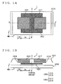
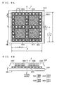
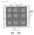
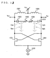
- Differentialoszillationsschaltung (7) mit einem Differentialkondensator (1, 2, 3), umfassend eine Mehrzahl von Kondensatoren (1003 und 1004, 2002 bis 2004, oder 3001 bis 3004), welche jeweils eine obere Elektrode (1015, 1017) und eine untere Elektrode (1016, 1018) aufweisen, welche zueinander parallel entlang einer vertikalen Richtung sind, weiterhin umfassend zumindest einen mit jeder unteren Elektrode (1016, 1018) verbundenen variablen Kondensator (1005 oder 1006) oder zumindest einen mit jeder oberen Elektrode (1015, 1017) verbundenen variablen Kondensator (1005 oder 1006),
wobei
jeder einzelne der Mehrzahl der Kondensatoren (1003 und 1004, 2002 bis 2004, oder 3001 bis 3004) auf einem Halbleitersubstrat (1020) in einer symmetrischen Position gegenüber einem anderen der Mehrzahl der Kondensatoren (1003 und 1004, 2002 bis 2004, oder 3001 bis 3004) bezüglich einer vertikalen Ebene (B-B') gebildet ist,
der Differentialkondensator (1,2,3) weiterhin eine zwischen jeder unteren Elektrode (1016, 1018) und dem Halbleitersubstrat (1020) eingefügte Abschirmplatte (1022 bis 1024, 2005 oder 3005) umfasst,
die Abschirmplatte (1022 bis 1024, 2005 oder 3005) über eine Induktivität und/oder einen Widerstand geerdet ist, und
wenn jede untere Elektrode (1016 bis 1018) auf die Abschirmplatte (1022 bis 1024, 2005 oder 3005) in der vertikalen Richtung projiziert wird,
dadurch gekennzeichnet, dass
jede projizierte untere Elektrode (1016, 1018) eine teilweise Überlappung mit der Abschirmplatte (1022 bis 1024, 2005 oder 3005) aufweist,
wobei die teilweise Überlappung jeder projizierten unteren Elektrode (1016, 1018) mit der Abschirmplatte (1022 bis 1024, 2005 oder 3005) größer als 0 % und kleiner oder gleich 70 % einer Fläche der unteren Elektrode (1016, 1018) gewählt ist. - Differentialoszillationsschaltung (7) nach Anspruch 1, wobei jede projizierte untere Elektrode (1016, 1018) sich außerhalb der Abschirmplatte (1022 bis 1024, 2005 oder 3005) erstreckt.
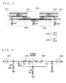
- Differentialoszillationsschaltung (7) nach Anspruch 1, wobei die Abschirmplatte (1023) einen darin gebildeten Schlitz (10231) aufweist.
- Differentialoszillationsschaltung (7) nach Anspruch 3, wobei der Schlitz (10231) die vertikale Ebene (B-B') schneidet.
- Differentialoszillationsschaltung (7) nach Anspruch 1, wobei die Abschirmplatte (1024) eine Mehrzahl von darin gebildeten Durchgangslöchern (10241, 20051) aufweist.
- Differentialoszillationsschaltung (7) nach Anspruch 5, wobei
die Mehrzahl von Durchgangslöchern (10241, 20051) entlang zweier vorbestimmter Richtungen in einem gleichen Intervall angeordnet ist, und
das Intervall zwischen Nachbarn der Mehrzahl der Durchgangslöcher (10241, 20051) gleich einem ganzzahligen Vielfachen einer halben Wellenlänge von stehenden Wellen ist, welche sich durch die Abschirmplatte (1022 bis 1024, 2005 oder 3005) ausbreiten. - Differentialoszillationsschaltung (7) nach Anspruch 6, wobei ein Abstand von zwei vorbestimmten Seiten der Abschirmplatte (1022 bis 1024, 2005 oder 3005) zur vertikalen Ebene (B-B') gleich einer Summe eines ganzzahligen Vielfachen der halben Wellenlänge der stehenden Wellen und einem Viertel der Wellenlänge der stehenden Wellen ist.
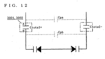
- Differentialoszillationsschaltung (7) nach Anspruch 1, wobei unter der Mehrzahl der Kondensatoren (1003 und 1004, 2002 bis 2004, oder 3001 bis 3004) beliebige zwei zueinander benachbarte Kondensatoren (1003 und 1004, 2002 bis 2004, oder 3001 bis 3004) jeweils ein phasengleiches Signal und ein Gegenphasensignal, welche ein Differentialsignalpaar bilden, empfangen.
- Differentialoszillationsschaltung (7) nach Anspruch 1, wobei ein Abschnitt der Abschirmplatte (1022 bis 1024, 2005 oder 3005), welcher die vertikale Ebene (B-B') schneidet, geerdet ist.
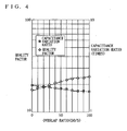
- Differentialoszillationsschaltung (7) nach Anspruch 1, wobei die Fläche der teilweisen Überlappung jeder projizierten unteren Elektrode (1016, 1018) mit der Abschirmplatte (1022 bis 1024, 2005 oder 3005) auf der Grundlage eines Kapazitätsvariationsverhältnisses der Schaltung des variablen Kondensators (1005, 1006) und eines Qualitätsfaktors jedes Kondensators bestimmt ist.
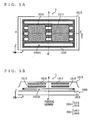
- Differentialoszillationsschaltung (7) nach Anspruch 1, wobei
ein Erster (2002) der Mehrzahl der Kondensatoren (1003 und 1004, 2002 bis 2004 oder 3001 bis 3004) auf dem Halbleitersubstrat (1020) in einer symmetrischen Position gegenüber einem der Mehrzahl der Kondensatoren (1003 und 1004, 2002 bis 2004, oder 3001 bis 3004) bezüglich der vertikalen Ebene (B-B') gebildet ist,
ein Zweiter (2003) der Mehrzahl der Kondensatoren (1003 und 1004, 2002 bis 2004, 3001 bis 3004) auf dem Halbleitersubstrat (1020) in einer symmetrischen Position gegenüber dem einen Kondensator bezüglich einer weiteren vertikalen Ebene gebildet ist, welche senkrecht zur vertikalen Ebene (B-B') liegt, und
ein Dritter (2004) der Mehrzahl der Kondensatoren (1003 und 1004, 2002 bis 2004, 3001 bis 3004) auf dem Halbleitersubstrat (1020) in einer symmetrischen Position gegenüber dem einen Kondensator bezüglich einer Schnittlinie zwischen der vertikalen Ebene (B-B') und der weiteren vertikalen Ebene gebildet ist. - Differentialoszillationsschaltung (7) nach Anspruch 11, wobei ein phasengleiches Signal und ein Gegenphasensignal, welche ein Differentialsignalpaar bilden, an die Mehrzahl der Kondensatoren (1003 und 1004, 2002 bis 2004, oder 3001 bis 3004) derart geliefert werden, dass eines aus dem phasengleichen Signal oder dem Gegenphasensignal sowohl an den einen Kondensator (2002) als auch an den dritten Kondensator (2004) geliefert wird, und dass das andere aus dem phasengleichen Signal oder dem Gegenphasensignal, sowohl an den ersten (2002) als auch an den zweiten Kondensator (2003) geliefert wird.
- Differentialoszillationsschaltung (7) nach Anspruch 11, wobei
die Abschirmplatte (1022 bis 1024, 2005 oder 3005) eine Mehrzahl von darin gebildeten Durchgangslöchern (10241, 20051) aufweist, wobei die Durchgangslöcher (10241, 20051) entlang zweier vorbestimmter Richtungen in einem gleichen Intervall angeordnet sind, so dass das Intervall zwischen Nachbarn aus der Mehrzahl der Durchgangslöcher (10241, 20051) im Wesentlichen gleich einem ganzzahligen Vielfachen einer halben Wellenlänge von stehenden Wellen ist, welche sich durch die Abschirmplatte (1022 bis 1024, 2005 oder 3005) ausbreiten, und
die Abschirmplatte (1022 bis 1024, 2005 oder 3005) eine im Wesentlichen rechteckige Form aufweist, so dass ein Abstand von zwei vorbestimmten Seiten der Abschirmplatte (1022 bis 1024, 2005 oder 3005) zur vertikalen Ebene (B-B') und ein Abstand von den anderen beiden Seiten der Abschirmplatte (1022 bis 1024, 2005 oder 3005) zur weiteren vertikalen Ebene jeweils im Wesentlichen gleich einer Summe eines ganzzahligen Vielfachen der halben Wellenlänge der stehenden Wellen und einem Viertel der Wellenlänge der stehenden Wellen sind.
Applications Claiming Priority (2)
| Application Number | Priority Date | Filing Date | Title |
|---|---|---|---|
| JP2003191267 | 2003-07-03 | ||
| JP2003191267 | 2003-07-03 |
Publications (3)
| Publication Number | Publication Date |
|---|---|
| EP1496528A2 EP1496528A2 (de) | 2005-01-12 |
| EP1496528A3 EP1496528A3 (de) | 2009-07-22 |
| EP1496528B1 true EP1496528B1 (de) | 2012-09-05 |
Family
ID=33447963
Family Applications (1)
| Application Number | Title | Priority Date | Filing Date |
|---|---|---|---|
| EP04015456A Not-in-force EP1496528B1 (de) | 2003-07-03 | 2004-07-01 | Differentieller Schwingkreis |
Country Status (3)
| Country | Link |
|---|---|
| US (1) | US6940707B2 (de) |
| EP (1) | EP1496528B1 (de) |
| CN (1) | CN100426505C (de) |
Families Citing this family (11)
| Publication number | Priority date | Publication date | Assignee | Title |
|---|---|---|---|---|
| US7336475B2 (en) * | 2006-02-22 | 2008-02-26 | Vishay Vitramon, Inc. | High voltage capacitors |
| US8238075B2 (en) * | 2006-02-22 | 2012-08-07 | Vishay Sprague, Inc. | High voltage capacitors |
| WO2009108756A1 (en) * | 2008-02-26 | 2009-09-03 | Softspikes, Llc | Improved traction cleat for field sports |
| WO2011033659A1 (ja) * | 2009-09-18 | 2011-03-24 | 株式会社 東芝 | 無線機 |
| US9054069B2 (en) * | 2013-09-05 | 2015-06-09 | International Business Machines Corporation | Variable capacitance integrated circuit |
| TWI500934B (zh) * | 2013-09-11 | 2015-09-21 | Pixart Imaging Inc | 具有對稱差分電容的微機電元件 |
| US9739816B2 (en) * | 2013-11-27 | 2017-08-22 | Analog Devices, Inc. | Capacitive sensor with differential shield |
| CN105338399A (zh) * | 2015-10-29 | 2016-02-17 | 小米科技有限责任公司 | 图像获取方法及装置 |
| IL253252B (en) * | 2016-07-28 | 2021-05-31 | Neteera Tech Ltd | Terahertz detector in Simos technology |
| CN110323334B (zh) * | 2019-07-09 | 2023-03-24 | 四川中微芯成科技有限公司 | 一种用寄生电容做adc电容的结构及方法 |
| CN116632001B (zh) * | 2023-07-24 | 2023-10-13 | 合肥晶合集成电路股份有限公司 | 一种半导体装置及半导体装置的设计辅助装置 |
Citations (1)
| Publication number | Priority date | Publication date | Assignee | Title |
|---|---|---|---|---|
| JP2005159280A (ja) * | 2003-07-03 | 2005-06-16 | Matsushita Electric Ind Co Ltd | 差動容量素子、差動アンテナ素子及び差動共振素子 |
Family Cites Families (20)
| Publication number | Priority date | Publication date | Assignee | Title |
|---|---|---|---|---|
| US201846A (en) * | 1878-03-26 | Improvement in beer-pumps | ||
| US171115A (en) * | 1875-12-14 | Improvement in millstones | ||
| US5220483A (en) | 1992-01-16 | 1993-06-15 | Crystal Semiconductor | Tri-level capacitor structure in switched-capacitor filter |
| JP2980142B2 (ja) | 1992-12-10 | 1999-11-22 | 富士通株式会社 | 半導体容量素子およびこれを用いた回路 |
| US5760456A (en) * | 1995-12-21 | 1998-06-02 | Grzegorek; Andrew Z. | Integrated circuit compatible planar inductors with increased Q |
| US6100750A (en) * | 1996-08-29 | 2000-08-08 | U.S. Philips Corporation | Frequency-independent voltage divider |
| US6366443B1 (en) * | 1997-12-09 | 2002-04-02 | Daniel Devoe | Ceramic chip capacitor of conventional volume and external form having increased capacitance from use of closely-spaced interior conductive planes reliably connecting to positionally-tolerant exterior pads through multiple redundant vias |
| US6066537A (en) * | 1998-02-02 | 2000-05-23 | Tritech Microelectronics, Ltd. | Method for fabricating a shielded multilevel integrated circuit capacitor |
| US6097195A (en) * | 1998-06-02 | 2000-08-01 | Lucent Technologies Inc. | Methods and apparatus for increasing metal density in an integrated circuit while also reducing parasitic capacitance |
| JP2000251379A (ja) * | 1999-02-24 | 2000-09-14 | Mitsumi Electric Co Ltd | 大容量磁気ディスク装置 |
| JP3398693B2 (ja) * | 1999-08-24 | 2003-04-21 | エヌイーシーマイクロシステム株式会社 | 半導体記憶装置 |
| US6489663B2 (en) * | 2001-01-02 | 2002-12-03 | International Business Machines Corporation | Spiral inductor semiconducting device with grounding strips and conducting vias |
| JP4047064B2 (ja) | 2001-05-17 | 2008-02-13 | 松下電器産業株式会社 | 高周波半導体装置 |
| US6903459B2 (en) * | 2001-05-17 | 2005-06-07 | Matsushita Electric Industrial Co., Ltd. | High frequency semiconductor device |
| US6456481B1 (en) * | 2001-05-31 | 2002-09-24 | Greatbatch-Sierra, Inc. | Integrated EMI filter-DC blocking capacitor |
| JP3977053B2 (ja) * | 2001-10-30 | 2007-09-19 | 富士通株式会社 | 容量素子及びその製造方法 |
| JP3842111B2 (ja) * | 2001-11-13 | 2006-11-08 | 富士通株式会社 | 半導体装置及びその製造方法 |
| JP2003188338A (ja) * | 2001-12-13 | 2003-07-04 | Sony Corp | 回路基板装置及びその製造方法 |
| JP3748556B2 (ja) | 2002-03-15 | 2006-02-22 | 松下電器産業株式会社 | 平衡型高周波デバイス |
| EP1505728A3 (de) | 2002-03-15 | 2011-12-07 | Panasonic Corporation | Symmetrisches Hochfrequenz-Bauelement, Schaltkreis und Verfahren zur Verbesserung der Signalsymmetrie |
-
2004
- 2004-07-01 EP EP04015456A patent/EP1496528B1/de not_active Not-in-force
- 2004-07-01 US US10/880,531 patent/US6940707B2/en active Active - Reinstated
- 2004-07-05 CN CNB200410062884XA patent/CN100426505C/zh not_active Expired - Fee Related
Patent Citations (1)
| Publication number | Priority date | Publication date | Assignee | Title |
|---|---|---|---|---|
| JP2005159280A (ja) * | 2003-07-03 | 2005-06-16 | Matsushita Electric Ind Co Ltd | 差動容量素子、差動アンテナ素子及び差動共振素子 |
Also Published As
| Publication number | Publication date |
|---|---|
| EP1496528A2 (de) | 2005-01-12 |
| CN1577857A (zh) | 2005-02-09 |
| US6940707B2 (en) | 2005-09-06 |
| EP1496528A3 (de) | 2009-07-22 |
| US20050002149A1 (en) | 2005-01-06 |
| CN100426505C (zh) | 2008-10-15 |
Similar Documents
| Publication | Publication Date | Title |
|---|---|---|
| US6331930B1 (en) | Multilayer capacitor, electronic device and high frequency circuit using the same | |
| EP1496528B1 (de) | Differentieller Schwingkreis | |
| US6226169B1 (en) | Multilayer capacitor | |
| JP4024572B2 (ja) | インタディジタルキャパシタを有するデバイス | |
| US5023578A (en) | Filter array having a plurality of capacitance elements | |
| EP0917165B1 (de) | Vielschichtkondensator | |
| US20070109709A1 (en) | Internally shielded energy conditioner | |
| FI113583B (fi) | Dielektrinen resonaattori ja menetelmä sen valmistamiseksi | |
| KR20090033177A (ko) | 개선된 금속-절연체-금속 캐패시터 | |
| US20150131203A1 (en) | Electronic devices with floating metal rings | |
| US4894629A (en) | Bandpass filter having magnetically coupled resonators | |
| JPH11214256A (ja) | 積層3端子コンデンサアレイ | |
| US6922126B1 (en) | Inductor element | |
| US8860531B2 (en) | Filter having electrical circuit arrangement with concentrated elements in multi-layer substrates | |
| US20050285660A1 (en) | Frequency-independent voltage divider | |
| US20060091443A1 (en) | Composite capacitor | |
| JPH06204397A (ja) | 複合電子部品 | |
| US20220131522A1 (en) | Resonator and filter | |
| US7030443B2 (en) | MIM capacitor | |
| JP4933036B2 (ja) | 差動容量素子、差動アンテナ素子及び差動共振素子 | |
| JP3547008B2 (ja) | 集積回路装置 | |
| US6636108B2 (en) | Filter circuit and electronic device using the same | |
| EP1587135A1 (de) | Schraubenlinienförmiger Induktor | |
| EP0874456A1 (de) | Piezoelektrischer Resonator und elektronisches Bauteil damit | |
| JP4013734B2 (ja) | Mim容量 |
Legal Events
| Date | Code | Title | Description |
|---|---|---|---|
| PUAI | Public reference made under article 153(3) epc to a published international application that has entered the european phase |
Free format text: ORIGINAL CODE: 0009012 |
|
| AK | Designated contracting states |
Kind code of ref document: A2 Designated state(s): AT BE BG CH CY CZ DE DK EE ES FI FR GB GR HU IE IT LI LU MC NL PL PT RO SE SI SK TR |
|
| AX | Request for extension of the european patent |
Extension state: AL HR LT LV MK |
|
| RIN1 | Information on inventor provided before grant (corrected) |
Inventor name: ADACHI, HISASHI Inventor name: NAKATANI, TOSHIFUMI Inventor name: NAKANISHI, KAYO,6-1-35, KOAZA HORIJIRI |
|
| RAP1 | Party data changed (applicant data changed or rights of an application transferred) |
Owner name: PANASONIC CORPORATION |
|
| RIC1 | Information provided on ipc code assigned before grant |
Ipc: H01L 23/522 20060101ALI20090320BHEP Ipc: H01P 7/08 20060101ALI20090320BHEP Ipc: H01Q 9/06 20060101ALI20090320BHEP Ipc: H01Q 9/04 20060101ALI20090320BHEP Ipc: H01L 23/64 20060101AFI20090320BHEP |
|
| PUAL | Search report despatched |
Free format text: ORIGINAL CODE: 0009013 |
|
| AK | Designated contracting states |
Kind code of ref document: A3 Designated state(s): AT BE BG CH CY CZ DE DK EE ES FI FR GB GR HU IE IT LI LU MC NL PL PT RO SE SI SK TR |
|
| AX | Request for extension of the european patent |
Extension state: AL HR LT LV MK |
|
| 17P | Request for examination filed |
Effective date: 20091028 |
|
| AKX | Designation fees paid |
Designated state(s): AT BE BG CH CY CZ DE DK EE ES FI FR GB GR HU IE IT LI LU MC NL PL PT RO SE SI SK TR |
|
| 17Q | First examination report despatched |
Effective date: 20100709 |
|
| GRAP | Despatch of communication of intention to grant a patent |
Free format text: ORIGINAL CODE: EPIDOSNIGR1 |
|
| GRAS | Grant fee paid |
Free format text: ORIGINAL CODE: EPIDOSNIGR3 |
|
| GRAA | (expected) grant |
Free format text: ORIGINAL CODE: 0009210 |
|
| RIN1 | Information on inventor provided before grant (corrected) |
Inventor name: NAKANISHI, KAYO Inventor name: NAKATANI, TOSHIFUMI Inventor name: ADACHI, HISASHI |
|
| AK | Designated contracting states |
Kind code of ref document: B1 Designated state(s): AT BE BG CH CY CZ DE DK EE ES FI FR GB GR HU IE IT LI LU MC NL PL PT RO SE SI SK TR |
|
| REG | Reference to a national code |
Ref country code: GB Ref legal event code: FG4D |
|
| REG | Reference to a national code |
Ref country code: CH Ref legal event code: EP |
|
| REG | Reference to a national code |
Ref country code: AT Ref legal event code: REF Ref document number: 574461 Country of ref document: AT Kind code of ref document: T Effective date: 20120915 |
|
| REG | Reference to a national code |
Ref country code: IE Ref legal event code: FG4D |
|
| REG | Reference to a national code |
Ref country code: DE Ref legal event code: R096 Ref document number: 602004039188 Country of ref document: DE Effective date: 20121031 |
|
| REG | Reference to a national code |
Ref country code: AT Ref legal event code: MK05 Ref document number: 574461 Country of ref document: AT Kind code of ref document: T Effective date: 20120905 |
|
| REG | Reference to a national code |
Ref country code: NL Ref legal event code: VDEP Effective date: 20120905 |
|
| PG25 | Lapsed in a contracting state [announced via postgrant information from national office to epo] |
Ref country code: AT Free format text: LAPSE BECAUSE OF FAILURE TO SUBMIT A TRANSLATION OF THE DESCRIPTION OR TO PAY THE FEE WITHIN THE PRESCRIBED TIME-LIMIT Effective date: 20120905 Ref country code: CY Free format text: LAPSE BECAUSE OF FAILURE TO SUBMIT A TRANSLATION OF THE DESCRIPTION OR TO PAY THE FEE WITHIN THE PRESCRIBED TIME-LIMIT Effective date: 20120905 Ref country code: FI Free format text: LAPSE BECAUSE OF FAILURE TO SUBMIT A TRANSLATION OF THE DESCRIPTION OR TO PAY THE FEE WITHIN THE PRESCRIBED TIME-LIMIT Effective date: 20120905 |
|
| PG25 | Lapsed in a contracting state [announced via postgrant information from national office to epo] |
Ref country code: SE Free format text: LAPSE BECAUSE OF FAILURE TO SUBMIT A TRANSLATION OF THE DESCRIPTION OR TO PAY THE FEE WITHIN THE PRESCRIBED TIME-LIMIT Effective date: 20120905 Ref country code: GR Free format text: LAPSE BECAUSE OF FAILURE TO SUBMIT A TRANSLATION OF THE DESCRIPTION OR TO PAY THE FEE WITHIN THE PRESCRIBED TIME-LIMIT Effective date: 20121206 Ref country code: SI Free format text: LAPSE BECAUSE OF FAILURE TO SUBMIT A TRANSLATION OF THE DESCRIPTION OR TO PAY THE FEE WITHIN THE PRESCRIBED TIME-LIMIT Effective date: 20120905 |
|
| PG25 | Lapsed in a contracting state [announced via postgrant information from national office to epo] |
Ref country code: EE Free format text: LAPSE BECAUSE OF FAILURE TO SUBMIT A TRANSLATION OF THE DESCRIPTION OR TO PAY THE FEE WITHIN THE PRESCRIBED TIME-LIMIT Effective date: 20120905 Ref country code: ES Free format text: LAPSE BECAUSE OF FAILURE TO SUBMIT A TRANSLATION OF THE DESCRIPTION OR TO PAY THE FEE WITHIN THE PRESCRIBED TIME-LIMIT Effective date: 20121216 Ref country code: BE Free format text: LAPSE BECAUSE OF FAILURE TO SUBMIT A TRANSLATION OF THE DESCRIPTION OR TO PAY THE FEE WITHIN THE PRESCRIBED TIME-LIMIT Effective date: 20120905 Ref country code: NL Free format text: LAPSE BECAUSE OF FAILURE TO SUBMIT A TRANSLATION OF THE DESCRIPTION OR TO PAY THE FEE WITHIN THE PRESCRIBED TIME-LIMIT Effective date: 20120905 Ref country code: RO Free format text: LAPSE BECAUSE OF FAILURE TO SUBMIT A TRANSLATION OF THE DESCRIPTION OR TO PAY THE FEE WITHIN THE PRESCRIBED TIME-LIMIT Effective date: 20120905 Ref country code: CZ Free format text: LAPSE BECAUSE OF FAILURE TO SUBMIT A TRANSLATION OF THE DESCRIPTION OR TO PAY THE FEE WITHIN THE PRESCRIBED TIME-LIMIT Effective date: 20120905 |
|
| PG25 | Lapsed in a contracting state [announced via postgrant information from national office to epo] |
Ref country code: PL Free format text: LAPSE BECAUSE OF FAILURE TO SUBMIT A TRANSLATION OF THE DESCRIPTION OR TO PAY THE FEE WITHIN THE PRESCRIBED TIME-LIMIT Effective date: 20120905 Ref country code: SK Free format text: LAPSE BECAUSE OF FAILURE TO SUBMIT A TRANSLATION OF THE DESCRIPTION OR TO PAY THE FEE WITHIN THE PRESCRIBED TIME-LIMIT Effective date: 20120905 Ref country code: PT Free format text: LAPSE BECAUSE OF FAILURE TO SUBMIT A TRANSLATION OF THE DESCRIPTION OR TO PAY THE FEE WITHIN THE PRESCRIBED TIME-LIMIT Effective date: 20130107 |
|
| PLBE | No opposition filed within time limit |
Free format text: ORIGINAL CODE: 0009261 |
|
| STAA | Information on the status of an ep patent application or granted ep patent |
Free format text: STATUS: NO OPPOSITION FILED WITHIN TIME LIMIT |
|
| PG25 | Lapsed in a contracting state [announced via postgrant information from national office to epo] |
Ref country code: DK Free format text: LAPSE BECAUSE OF FAILURE TO SUBMIT A TRANSLATION OF THE DESCRIPTION OR TO PAY THE FEE WITHIN THE PRESCRIBED TIME-LIMIT Effective date: 20120905 Ref country code: BG Free format text: LAPSE BECAUSE OF FAILURE TO SUBMIT A TRANSLATION OF THE DESCRIPTION OR TO PAY THE FEE WITHIN THE PRESCRIBED TIME-LIMIT Effective date: 20121205 |
|
| 26N | No opposition filed |
Effective date: 20130606 |
|
| PG25 | Lapsed in a contracting state [announced via postgrant information from national office to epo] |
Ref country code: IT Free format text: LAPSE BECAUSE OF FAILURE TO SUBMIT A TRANSLATION OF THE DESCRIPTION OR TO PAY THE FEE WITHIN THE PRESCRIBED TIME-LIMIT Effective date: 20120905 |
|
| REG | Reference to a national code |
Ref country code: DE Ref legal event code: R097 Ref document number: 602004039188 Country of ref document: DE Effective date: 20130606 |
|
| PG25 | Lapsed in a contracting state [announced via postgrant information from national office to epo] |
Ref country code: MC Free format text: LAPSE BECAUSE OF FAILURE TO SUBMIT A TRANSLATION OF THE DESCRIPTION OR TO PAY THE FEE WITHIN THE PRESCRIBED TIME-LIMIT Effective date: 20120905 |
|
| REG | Reference to a national code |
Ref country code: CH Ref legal event code: PL |
|
| REG | Reference to a national code |
Ref country code: IE Ref legal event code: MM4A |
|
| PG25 | Lapsed in a contracting state [announced via postgrant information from national office to epo] |
Ref country code: CH Free format text: LAPSE BECAUSE OF NON-PAYMENT OF DUE FEES Effective date: 20130731 Ref country code: LI Free format text: LAPSE BECAUSE OF NON-PAYMENT OF DUE FEES Effective date: 20130731 |
|
| PG25 | Lapsed in a contracting state [announced via postgrant information from national office to epo] |
Ref country code: IE Free format text: LAPSE BECAUSE OF NON-PAYMENT OF DUE FEES Effective date: 20130701 |
|
| PG25 | Lapsed in a contracting state [announced via postgrant information from national office to epo] |
Ref country code: TR Free format text: LAPSE BECAUSE OF FAILURE TO SUBMIT A TRANSLATION OF THE DESCRIPTION OR TO PAY THE FEE WITHIN THE PRESCRIBED TIME-LIMIT Effective date: 20120905 |
|
| PG25 | Lapsed in a contracting state [announced via postgrant information from national office to epo] |
Ref country code: LU Free format text: LAPSE BECAUSE OF NON-PAYMENT OF DUE FEES Effective date: 20130701 Ref country code: HU Free format text: LAPSE BECAUSE OF FAILURE TO SUBMIT A TRANSLATION OF THE DESCRIPTION OR TO PAY THE FEE WITHIN THE PRESCRIBED TIME-LIMIT; INVALID AB INITIO Effective date: 20040701 |
|
| REG | Reference to a national code |
Ref country code: FR Ref legal event code: PLFP Year of fee payment: 13 |
|
| REG | Reference to a national code |
Ref country code: FR Ref legal event code: PLFP Year of fee payment: 14 |
|
| REG | Reference to a national code |
Ref country code: FR Ref legal event code: PLFP Year of fee payment: 15 |
|
| PGFP | Annual fee paid to national office [announced via postgrant information from national office to epo] |
Ref country code: DE Payment date: 20190719 Year of fee payment: 16 Ref country code: FR Payment date: 20190719 Year of fee payment: 16 |
|
| PGFP | Annual fee paid to national office [announced via postgrant information from national office to epo] |
Ref country code: GB Payment date: 20190719 Year of fee payment: 16 |
|
| REG | Reference to a national code |
Ref country code: DE Ref legal event code: R119 Ref document number: 602004039188 Country of ref document: DE |
|
| GBPC | Gb: european patent ceased through non-payment of renewal fee |
Effective date: 20200701 |
|
| PG25 | Lapsed in a contracting state [announced via postgrant information from national office to epo] |
Ref country code: GB Free format text: LAPSE BECAUSE OF NON-PAYMENT OF DUE FEES Effective date: 20200701 Ref country code: FR Free format text: LAPSE BECAUSE OF NON-PAYMENT OF DUE FEES Effective date: 20200731 |
|
| PG25 | Lapsed in a contracting state [announced via postgrant information from national office to epo] |
Ref country code: DE Free format text: LAPSE BECAUSE OF NON-PAYMENT OF DUE FEES Effective date: 20210202 |