EP1487073A2 - Halterung eines Halbleiterlasers mittels löten - Google Patents
Halterung eines Halbleiterlasers mittels löten Download PDFInfo
- Publication number
- EP1487073A2 EP1487073A2 EP04253398A EP04253398A EP1487073A2 EP 1487073 A2 EP1487073 A2 EP 1487073A2 EP 04253398 A EP04253398 A EP 04253398A EP 04253398 A EP04253398 A EP 04253398A EP 1487073 A2 EP1487073 A2 EP 1487073A2
- Authority
- EP
- European Patent Office
- Prior art keywords
- semiconductor laser
- mounting
- laser device
- mounting substrate
- solder
- Prior art date
- Legal status (The legal status is an assumption and is not a legal conclusion. Google has not performed a legal analysis and makes no representation as to the accuracy of the status listed.)
- Withdrawn
Links
Images


Classifications
-
- H—ELECTRICITY
- H01—ELECTRIC ELEMENTS
- H01S—DEVICES USING THE PROCESS OF LIGHT AMPLIFICATION BY STIMULATED EMISSION OF RADIATION [LASER] TO AMPLIFY OR GENERATE LIGHT; DEVICES USING STIMULATED EMISSION OF ELECTROMAGNETIC RADIATION IN WAVE RANGES OTHER THAN OPTICAL
- H01S5/00—Semiconductor lasers
- H01S5/02—Structural details or components not essential to laser action
- H01S5/022—Mountings; Housings
- H01S5/0235—Method for mounting laser chips
- H01S5/02355—Fixing laser chips on mounts
- H01S5/0237—Fixing laser chips on mounts by soldering
-
- H—ELECTRICITY
- H01—ELECTRIC ELEMENTS
- H01S—DEVICES USING THE PROCESS OF LIGHT AMPLIFICATION BY STIMULATED EMISSION OF RADIATION [LASER] TO AMPLIFY OR GENERATE LIGHT; DEVICES USING STIMULATED EMISSION OF ELECTROMAGNETIC RADIATION IN WAVE RANGES OTHER THAN OPTICAL
- H01S5/00—Semiconductor lasers
- H01S5/02—Structural details or components not essential to laser action
- H01S5/022—Mountings; Housings
- H01S5/0233—Mounting configuration of laser chips
- H01S5/0234—Up-side down mountings, e.g. Flip-chip, epi-side down mountings or junction down mountings
-
- H—ELECTRICITY
- H01—ELECTRIC ELEMENTS
- H01S—DEVICES USING THE PROCESS OF LIGHT AMPLIFICATION BY STIMULATED EMISSION OF RADIATION [LASER] TO AMPLIFY OR GENERATE LIGHT; DEVICES USING STIMULATED EMISSION OF ELECTROMAGNETIC RADIATION IN WAVE RANGES OTHER THAN OPTICAL
- H01S5/00—Semiconductor lasers
- H01S5/02—Structural details or components not essential to laser action
- H01S5/022—Mountings; Housings
- H01S5/0235—Method for mounting laser chips
- H01S5/02375—Positioning of the laser chips
-
- H—ELECTRICITY
- H01—ELECTRIC ELEMENTS
- H01S—DEVICES USING THE PROCESS OF LIGHT AMPLIFICATION BY STIMULATED EMISSION OF RADIATION [LASER] TO AMPLIFY OR GENERATE LIGHT; DEVICES USING STIMULATED EMISSION OF ELECTROMAGNETIC RADIATION IN WAVE RANGES OTHER THAN OPTICAL
- H01S5/00—Semiconductor lasers
- H01S5/02—Structural details or components not essential to laser action
- H01S5/024—Arrangements for thermal management
- H01S5/02469—Passive cooling, e.g. where heat is removed by the housing as a whole or by a heat pipe without any active cooling element like a TEC
-
- H—ELECTRICITY
- H01—ELECTRIC ELEMENTS
- H01S—DEVICES USING THE PROCESS OF LIGHT AMPLIFICATION BY STIMULATED EMISSION OF RADIATION [LASER] TO AMPLIFY OR GENERATE LIGHT; DEVICES USING STIMULATED EMISSION OF ELECTROMAGNETIC RADIATION IN WAVE RANGES OTHER THAN OPTICAL
- H01S5/00—Semiconductor lasers
- H01S5/40—Arrangement of two or more semiconductor lasers, not provided for in groups H01S5/02 - H01S5/30
- H01S5/4025—Array arrangements, e.g. constituted by discrete laser diodes or laser bar
Definitions
- the present invention relates to a semiconductor laser device and in particular relates to a semiconductor laser device wherein the construction of the semiconductor laser mounting substrate is improved and, in addition, the bonding strength of the solder with the semiconductor laser is improved.
- semiconductor lasers in particular, semiconductor laser devices wherein a one-dimensional LD array of a large number of laser diode (LD) elements arranged such that their respective light emission regions are arranged in straight-line fashion is employed as a light emission source have come to be frequently used as excitation sources of solid-state lasers such as YAG (yttrium aluminum garnet) lasers.
- LD laser diode
- YAG yttrium aluminum garnet
- FIG. 6 is a view showing the construction of a prior art semiconductor laser device constructed using this technique.
- the mounting substrate is indicated by the reference symbol 1 and a semiconductor laser 3 having LD stripes 6 and emitters 7 are joined with this mounting substrate 1 using solder 10.
- coolers 8 are provided with flow passages in their interior through which coolant is passed; however, they may also be replaced by heat sinks, which are not provided with the passages for the passage of coolant in their interior. In this specification both of these will be referred to as "coolers”.
- the first problem with the use of solder of low melting point is the matter of cost.
- low melting point solder the use of indium (In) or solder of two or more elements including In may be considered, in both cases the cost is very high.
- the operation of soldering is difficult and the reliability of the soldered condition is low.
- materials for the mounting substrate whose thermal expansion coefficient is close to that of the semiconductor laser for example silicon, silicon carbide, aluminum nitride or alumina may be considered, but these materials are also expensive. Also, since these materials are insulators, it is desirable that they should be formed with a metallic coating; however, if this is done, in addition to the material cost there is added to the cost of the metallic coating formation process, further increasing costs.
- uniform soldering in this case means "soldering that is uniform in regard to both electrical and thermal aspects". In regard to such uniform soldering, residual stress left after soldering presents an obstacle, lowering the strength of the joint and causing the development of regions that are non-uniform in electrical or thermal terms as a result of for example prolonged use or vibration.
- the present invention is applied to a semiconductor laser device constituted by soldering the semiconductor laser to the mounting surface of a mounting base; its basic feature is that a recess that permits inflow of solder in molten condition is provided in at least part of a portion corresponding to an end of the semiconductor laser and a fillet of solder that reinforces the mounting strength of the semiconductor laser with respect to the mounting base is formed in this recess.
- the semiconductor laser is arranged such that the emitter of this semiconductor laser does not overlap the recess of the mounting base and, further preferably, each of the electrode forming face, the emitter and the reflecting face constituting the resonator facing this emitter of this semiconductor laser are arranged so as not to overlap the recess of the mounting base.
- a mounting substrate may be adopted that is arranged interposed between the semiconductor laser and a cooler for removing the heat of this semiconductor laser.
- a mounting substrate may be employed whereof at least part of the outer periphery thereof is formed by punching or cutting using a press machine, with the male mold of the press machine arranged on the semiconductor laser mounting surface side of the mounting substrate.
- the recess for forming the fillet in the interior by inflow of molten solder may be formed by for example chemical etching or chemical half etching or cutting processing.
- a solder layer may be formed beforehand on at least one of the mounting surface of the mounting base or the surface of the semiconductor laser opposite to this mounting surface, the semiconductor laser may be soldered to the mounting surface by melting this solder and the fillet may also be arranged to be formed by inflow of solder in molten condition into the recess.
- the preformed solder layer may be formed by for example evaporation or plating.
- the material of the solder there may be employed for example Sn, an alloy of two or more elements including a material that forms eutectic crystals with Sn, In, or an alloy of two or more elements including In.
- a metallic coating may also be formed as base processing of the solder on at least the mounting surface of the mounting base.
- Ni, Pt or Cr may be employed as the material of this metallic coating.
- a typical semiconductor laser mounted on the mounting base may have the form of a semiconductor laser array including a plurality of emitters, the width along the direction transverse to the plurality of emitters being for example in the range 0.5 cm to 2 cm.
- the plurality of emitters are each arranged in positions so as not to overlap the recesses.
- the mounting base is a mounting substrate that is arranged interposed between the semiconductor laser and a cooler for removing the heat of this semiconductor laser, for example copper, a chemical compound of copper or a composite material of copper and copper oxide may be employed as the material thereof.
- silicon, silicon carbide, aluminum nitride or alumina material may be employed as the material of the mounting substrate and a metallic coating may be formed on at least one of the side faces of this mounting substrate.
- the mounting substrate may be a single substrate of a plurality of substrates formed simultaneously in the same plate member by a chemical etching step.
- substrates may be employed that are formed by being divided into individual substrates by punching or cutting by means of a press machine.
- individual substrates which are formed by being molded and divided into individual substrates by arranging a male mold of the press machine on the semiconductor laser mounting surface side of the plurality of mounting substrates formed in the plate member and punching or cutting at least part of the outer periphery of each mounting substrate using the press machine, may be employed as mounting substrates.
- letters, numbers, symbols or patterns may be formed on the mounting substrates by the chemical etching step or chemical half etching step. Such letters, numbers, symbols or patterns may be arranged so as to make it possible to identify at what location in the aforementioned same plate member the mounting substrate was formed.
- the soldering of the mounting substrate may also be effected by forming a solder layer also on the surface on the side of the cooler and simultaneously performing soldering of the mounting substrate onto this cooler and soldering of the semiconductor laser onto this mounting substrate.
- the position of arrangement of the mounting substrate on the cooler is preferably such that the surface of the mounting substrate on the laser beam emission side is at a location that is further towards the inside of the cooler than the surface of the cooler on the laser beam emission side. Also, the distance between the laser beam emission surface of the semiconductor laser and the surface of the mounting substrate on the laser beam emission side can be 50 ⁇ m or less.
- the "recesses” that are formed on the base (mounting substrate or substitute therefor, such as for example an outer covering member of the cooler) where the semiconductor laser is mounted according to the present invention are not particularly restricted as to shape and could be for example of a shape such as a groove, rebate, notch, or through-hole, so long as they permit inflow of molten solder. Also, there is no particular restriction as to their size (area occupied by the region where the recesses are formed in the surface where the mounting surface of the mounting base is provided), so long as it is possible to ensure a sufficient soldering area in the portions excluding the recesses (middle portion and the region surrounding it). Also, the recesses may be formed in a corridor shape corresponding to the overall external periphery of the mounted semiconductor laser, or may be formed so as to correspond to only a part of the external periphery of the semiconductor laser (for example two parallel sides).
- a technique can be provided that ensures uniform high bonding strength between the semiconductor laser and the mounting substrate by an improved construction whereby electrical and thermal coupling of the semiconductor laser with the cooler through the mounting substrate is achieved, while yet avoiding increased costs.
- the present invention by forming recesses such as grooves, dents, notches or through-holes in the semiconductor laser mounting surface of the mounting substrate, the strength of the soldering between the two ends of the semiconductor laser and the mounting substrate is increased and uniform soldering can be achieved, by collecting molten solder therein and forming a fillet of solder between the two ends of the semiconductor laser and the mounting substrate.
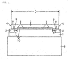
- Figure 1 shows an embodiment of the present invention in plan view seen from the direction of laser-beam emission.
- a mounting substrate indicated by reference numeral 1 is a mounting substrate that mounts a semiconductor laser 3.
- the semiconductor laser 3 constitutes a one-dimensional LD array.
- the semiconductor laser 3 (one-dimensional LD array) comprises a plurality of emitters 7 (light-emitting portions) that are divided by means of LD stripes 6; each emitter 7 emits a laser beam in the forwards direction in the direction perpendicular to the plane of the drawing of Figure 1.
- D in the Figure is the width of the semiconductor laser 3 along the direction transverse to the plurality of emitters 7 and is for example in the range 0.5 cm to 2 cm.
- a mounting substrate 1 is adopted having recesses constituted by grooves 2 in locations corresponding to the two ends of the semiconductor laser 3. As will be described, the recesses serve for forming solder fillets 9 by inflow of molten solder from apertures thereof on the semiconductor laser side.
- grooves 2 having a U-shaped cross section are shown, but there is no particular restriction to this form so long as solder fillets 9 can be formed that permit inflow of molten solder.
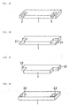
- Figure 2A to Figure 2D show four examples including an example of a mounting substrate (Figure 2A) having grooves 2 of this U-shaped cross section.
- Figure 2B shows an example in which the recesses are formed in the form of concaves 21
- Figure 2C shows an example in which the recesses are formed in the form of notches 22
- Figure 2D shows an example in which the recesses are formed in the form of through-holes 23, respectively.
- the grooves 2 are shown in a shape produced by cutting inwards in the depth direction up to a certain point but it would be possible to adopt a shape produced by cutting to the entire length in the depth direction.
- solder fillets 9 can be formed so long as at least a part thereof in the depth direction of the semiconductor laser 3 is arranged on a groove 2 or a recess substituting for this.
- the emitters 7 of the semiconductor laser 3 are formed avoiding locations directly above the recesses constituted by the grooves 2 at both ends of the mounting substrate 1 (as described with reference to Figure 2A to Figure 2D, the term “recess” is used to include, in addition to grooves 2, for example concaves 21, notches 22 or through-holes 23); the LD stripes 6 on the outermost side are positioned in positions further inwards by a distance d (for example of the order of a few hundred ⁇ m) from the edge 5 on the inside of each recess 2 at each end.
- d for example of the order of a few hundred ⁇ m
- the mounting of the semiconductor laser 3 on the mounting substrate 1 and the mounting of the mounting substrate 1 on the outer surface of the cooler 8 are in both cases performed by soldering. Performing soldering also between the mounting substrate 1 and the cooler 8 rather than merely performing soldering between the semiconductor laser 3 and the mounting substrate 1 is advantageous in improving electrical contact and thermal contact. Also, in this case, it is advantageous if the soldering of the semiconductor laser 3 and the mounting substrate 1 and the soldering of the mounting substrate 1 and the cooler 8 are performed simultaneously, so as not to increase the number of steps.
- solder 10 that is employed is formed beforehand on both surfaces (the surface on the side of the semiconductor laser 3 and the surface on the side of the cooler 8) of the mounting substrate 1; this can be achieved by for example evaporation or plating.
- some of the solder that is in a molten condition due to heating enters the interior of the grooves 2 from the vicinity of the grooves 2 (the vicinity of the electrodes at both ends of the semiconductor laser 3).
- the molten solder that has collected in the grooves 2 wets the inside wall of the grooves 2 and the electrodes at both ends of the semiconductor laser 3 that are arranged above the grooves 2 with the result that solder fillets 9 are formed on solidification. Thanks to this formation of fillets 9, the soldering at both ends of the semiconductor laser 3 is reinforced thereby, overall, for example making the bonding strength more uniform and making separation of the solder less likely.
- both side faces 4 of the semiconductor laser 3 are arranged exactly above the grooves 2 of the mounting substrate 1, the advantage is obtained that the possibility of solder adhering to the side faces 4 is reduced. That is, if solder adheres to the side faces 4 of the semiconductor laser 3, conduction takes place at these points, with the result that current does not flow to the emitters 7 and the laser beam is not emitted; however, if the side faces 4 are arranged directly above the grooves 2, the risk of solder adhering to the side faces 4 can be reduced.
- the bonding strength may deteriorate with lapse of time by the formation of intermetallic chemical compounds after soldering.
- An example of this deterioration is the case where a material including Sn is employed for the solder 10 and a material including copper is employed for the mounting substrate 1.
- a coating of for example Ni, Ti, Pt or Cr may be formed on the mounting substrate 1 as base processing of the solder 10.
- Flux is frequently employed in order to improve wettability by removing the oxide film at the surface of the solder during soldering.
- the laser beam emitting portions (emitters 7) of the semiconductor laser 3 are in positions that are extremely close to the solder 10 (for example no more than about 10 ⁇ m), so residual amounts of flux may adhere to the laser beam emitting portions. If the emitters 7 are contaminated by residual amounts of flux, the emitted beam is obstructed, risking a lowering of output. Also, corrosion of the laser-beam emission surfaces of the semiconductor laser may cause a lowering of reliability of the semiconductor laser device. It is therefore desirable to ensure that the effect of flux residues is substantially nil by for example employing a low residue type flux.
- soldering the mounting substrate 1 and the cooler 8 Another method of achieving this is the technique of employing hydrogen gas when soldering; if this is adopted, the oxide film at the surface of the solder is removed by the reductive action of the hydrogen, improving wettability and hence improving reliability of soldering. There is the advantage that the effect of flux residues is eliminated, since there is no need to employ flux.
- soldering the mounting substrate 1 and the cooler 8 the solder needs to wet and spread over the surface of the cooler, so, as already stated, solder is preferably applied beforehand by evaporation or plating at least to the surface of the cooler where the mounting substrate is to be mounted. However, if electrical contact and thermal contact can be ensured, soldering of the mounting substrate 1 and the cooler 8 is not necessarily essential.
- the “depth direction” means the direction of laser-beam emission (in Figure 1 this is the direction perpendicular to the plane of the drawing sheet, i.e. the direction perpendicular to the direction indicated by the width D).
- the length of the mounting substrate 1 in this laser-beam emission direction is preferably the same as the length of the semiconductor laser 3 in the depth direction, or exceeds this to some extent.
- the length of the cooler 8 in the depth direction is the same as the length of the mounting substrate 1 in the depth direction or exceeds this to some extent.
- the surface of the mounting substrate 1 on the laser-beam emission side is arranged at a distance somewhat further inwards than the surface on the laser-beam emission side of the cooler 8.
- the semiconductor laser 3 is arranged such that the distance between the laser-beam emission surface (light emission surface of the emitters 7) and the surface of the mounting substrate 1 on the laser-beam emission side is for example 50 ⁇ m or less.
- solder fillets 9 must be formed within the grooves 2, there are no particular restrictions regarding the mounting substrate or solder material in order to achieve this.
- copper which is inexpensive
- solder 10 SnPb eutectic solder, which is of excellent wettability and with which the soldering operation can be performed easily, may be employed. In this case, the reliability of the solder joints may be improved even though the cost is low. However, higher melting point solder may be employed, if wettability can be ensured.
- a copper mounting substrate and SnPb eutectic solder in view of cost aspects and ease of the soldering operation, in cases where the residual stress aspect is regarded as important, it is preferable to employ a material whose thermal expansion coefficient is close to that of the semiconductor laser for the mounting substrate and to employ a material of low melting point as the solder (so-called low melting point solder).
- a material whose thermal expansion coefficient is close to that of the semiconductor laser for the mounting substrate and to employ a material of low melting point as the solder (so-called low melting point solder).
- mounting substrates made of silicon, silicon carbide, aluminum nitride or alumina may be employed albeit they are more expensive than copper.
- preferably conductive processing is performed on the surface.
- low cost can be achieved by adopting a method of manufacture in which a plurality of mounting substrates are obtained. Also, by adopting a method of manufacture in which a plurality of these mounting substrates are obtained for the manufacture of a mounting substrate made of copper, even further reduction in costs can be achieved.
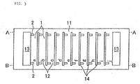
- FIG. 3 is a view given in explanation of an example of a method of manufacturing mounting substrates whereby a plurality of mounting substrates are obtained; in this case, an example is illustrated in which ten mounting substrates 1 are manufactured from a single plate member (for example copper sheet) 11, using a chemical etching step (or chemical half etching step). Specifically, rectangular apertures 13 on both sides of a plate member 11 and apertures 14 between adjacent mounting substrates 1 can be formed by a known chemical etching step and ten mounting substrates of the same shape and same dimensions obtained by performing cutting or punching substantially along the lines A-A and B-B.
- a chemical etching step or chemical half etching step
- the grooves 2 (or recesses such as dents, notches or through-holes substituting for these grooves) can also be formed simultaneously utilizing the chemical etching step (or chemical half etching step).
- Forming a plurality of mounting substrates in the same plate member 11 in this way is extremely advantageous in lowering manufacturing costs, enables a single mounting substrate 1 to be manufactured at low overall cost, even if an expensive material is adopted, and is even more advantageous if an inexpensive material such as copper is employed. Furthermore, it is possible to process a plurality of mounting substrates 1 at the same time by performing evaporation or plating of solder in the condition before the plate member 11 is cut.
- An individual mounting substrate 1 may be formed from the plate member 11 by cutting substantially along the lines A-A and B-B but the method of punching using a press machine is easy and inexpensive.
- Figure 4A to Figure 4D show an example of forming an individual mounting substrate from a plate member using press punching.
- a male mold 31 and female mold 32 are prepared.
- the width W of the outline of the outer periphery of the male mold 31 corresponds to the distance between the lines A-A and B-B shown in Figure 3.
- the length L of the outline of the outer periphery of the male mold 31 corresponds to the distance to the right-hand side edge of the substrate (reference symbol j) at the right-hand end from the left-hand edge of the substrate (reference symbol a) at the left-hand end shown in Figure 3.
- the plate member 11 is arranged on the female mold 32 such that the mounting surfaces of the mounting substrates face the male mold 31 and forming is effected by cutting or punching using a press machine (not shown).
- Figure 4C shows the condition in which cutting or punching for forming is effected (condition in which the male mold 31 has entered the interior of the aperture of the female mold 32).
- flash may be generated at the location of punching or at the location of cutting the mounting substrate 1. If such flash is present at a soldered joint, it lowers the reliability of the soldering.
- punching or cutting may be effected in a condition with the male mold 31 of the press machine arranged at the face of the mounting substrate 1 where the semiconductor laser is mounted, so that the width G (see Figure 4D) of the mounting substrate 1 is larger than the width D (see Figure 1) of the semiconductor laser 3.
- This technique is adopted in the example of Figure 4 described above.
- a plurality of mounting substrates are obtained from a single plate member 11
- the same press molding technique can of course be applied even in the case where only a single mounting substrate is obtained from a single plate member.
- the mounting substrate 1 that mounts the semiconductor laser 3 is arranged interposed between the semiconductor laser 3 and the cooler 8, it will be possible to apply the concept of the present invention also in the case where the semiconductor laser 3 is directly mounted on the cooler 8.
- Figure 5 shows an example thereof.
- the semiconductor laser 3 is a one-dimensional LD array.
- the semiconductor laser 3 (one-dimensional LD array) comprises a plurality of emitters 7 (light emission sections) that are divided by LD stripes 6; each emitter 7 emits a laser beam in the forwards direction in the direction perpendicular to the drawing sheet of this Figure 5.
- recesses On the upper surface of the cooler 8, in locations corresponding to the two ends of the semiconductor laser 3, there are formed recesses (grooves 2 or dents, notches or through-holes or the like substituting therefor). As described above, these grooves 2 serve to form fillets 9 of solder by inflow of molten solder from apertures on the side of the semiconductor laser and there is no particular restriction regarding their form so long as they permit inflow of molten solder and make possible the formation of solder fillets 9.
- the specific examples of recesses shown in Figure 2A to Figure 2D can also be applied to the case in which the cooler 8 itself is employed as a mounting substrate.
- the broken line shown in Figure 5 shows the case where the recesses are through-holes.
- the emitters 7 of the semiconductor laser 3 are formed avoiding locations directly above the grooves 2 at both ends of the semiconductor laser 3.
- the LD stripes 6 on the outermost side are positioned in positions further inwards by a distance d (for example of the order of a few hundred ⁇ m) from the edge 5 on the inside of each recess 2.
- d for example of the order of a few hundred ⁇ m
- the mounting of the semiconductor laser 3 on the outer surface of the cooler 8 is performed by soldering. Performing soldering between the semiconductor laser 3 and the cooler 8 is extremely advantageous in improving electrical contact and thermal contact between these two. It is convenient if the solder 10 that is employed is formed beforehand on the upper surface of the cooler 8 by for example evaporation or plating. During soldering of the semiconductor laser 3 and the cooler 8, some of the solder that is in a molten condition due to heating enters the interior of the grooves 2 from the vicinity of the grooves 2 (the vicinity of the electrodes at both ends of the semiconductor laser 3).
- solder fillets 9 are formed on solidification. Thanks to this formation of fillets 9, the soldering at both ends of the semiconductor laser 3 is reinforced thereby, overall, for example making the bonding strength more uniform and making separation of the solder less likely.
- both side faces 4 of the semiconductor laser 3 are arranged exactly above the grooves 2 of the mounting substrate 1, the advantage is obtained that the possibility of solder adhering to the side faces 4 is reduced.
- the bonding strength may deteriorate with lapse of time by the formation of intermetallic chemical compounds after soldering.
- a coating of for example Ni, Ti, Pt or Cr may be formed on the upper surface of the cooler 8 as base processing of the solder 10.
- the length of the cooler 8 (dimension in the direction perpendicular to the plane of Figure 5) is the same as the length of the semiconductor laser 3 in the depth direction or exceeds this to some extent.
- the semiconductor laser 3 is arranged such that the distance between the laser-beam emission surface (light emission surface of the emitters 7) and the surface of the cooler 8 on the laser-beam emission side is for example 50 ⁇ m or less.
- solder fillets 9 must be formed within the grooves 2, there are no particular restrictions regarding the upper surface of the cooler 8 or solder material in order to achieve this.
- the reinforcing effect of the fillets 9 is then somewhat reduced by comparatively large residual stress, there are no particular problems if copper, which is inexpensive and commonly used, is employed as the material of the cooler 8.
- solder 10 SnPb eutectic solder, which is of excellent wettability and with which the soldering operation can be performed easily, may be employed. In this case, the reliability of the solder joints may be improved even though the cost is low. However, higher melting point solder may be employed, if wettability can be ensured. In cases where the residual stress aspect is regarded as important, it is preferable to employ a material of low melting point as the solder (so-called low melting point solder).
- recesses such as grooves, dents, notches or through-holes are formed in the semiconductor laser mounting surface of the mounting substrate, thereby enabling the formation of solder fillets between the mounting substrate and both ends of the semiconductor laser by collection of molten solder therein and so increasing the bonding strength and enabling uniform bonding strength to be obtained over the entire semiconductor laser and mounting substrate.
- convenient processing techniques such as chemical etching, chemical half etching, or press processing, a plurality of mounting substrates that are employed as mounting bases can be manufactured from the same plate member, so a lowering of costs can be achieved.
Landscapes
- Physics & Mathematics (AREA)
- Condensed Matter Physics & Semiconductors (AREA)
- General Physics & Mathematics (AREA)
- Electromagnetism (AREA)
- Optics & Photonics (AREA)
- Semiconductor Lasers (AREA)
Applications Claiming Priority (2)
| Application Number | Priority Date | Filing Date | Title |
|---|---|---|---|
| JP2003167816A JP2005005511A (ja) | 2003-06-12 | 2003-06-12 | 半導体レーザ装置 |
| JP2003167816 | 2003-06-12 |
Publications (2)
| Publication Number | Publication Date |
|---|---|
| EP1487073A2 true EP1487073A2 (de) | 2004-12-15 |
| EP1487073A3 EP1487073A3 (de) | 2005-03-30 |
Family
ID=33296873
Family Applications (1)
| Application Number | Title | Priority Date | Filing Date |
|---|---|---|---|
| EP04253398A Withdrawn EP1487073A3 (de) | 2003-06-12 | 2004-06-08 | Halterung eines Halbleiterlasers mittels löten |
Country Status (3)
| Country | Link |
|---|---|
| US (1) | US20040252735A1 (de) |
| EP (1) | EP1487073A3 (de) |
| JP (1) | JP2005005511A (de) |
Cited By (1)
| Publication number | Priority date | Publication date | Assignee | Title |
|---|---|---|---|---|
| EP1675229A1 (de) * | 2004-12-24 | 2006-06-28 | Fanuc Ltd | Laserdiodenbarren mit Aussparungen zum optimalen Verlöten mit einer Wärmesenke |
Families Citing this family (7)
| Publication number | Priority date | Publication date | Assignee | Title |
|---|---|---|---|---|
| JP4969087B2 (ja) * | 2005-11-28 | 2012-07-04 | スタンレー電気株式会社 | 共晶ボンディング発光装置とその製造方法 |
| CA2718504A1 (en) * | 2008-03-14 | 2009-09-17 | Mitsubishi Electric Corporation | Optical module |
| DE102009035639B4 (de) * | 2009-07-31 | 2019-10-24 | Osram Opto Semiconductors Gmbh | Breitstreifenlaser mit einem epitaktischen Schichtenstapel und Verfahren zu dessen Herstellung |
| CA2928970C (en) * | 2013-11-01 | 2018-08-28 | Mitsubishi Electric Corporation | Semiconductor laser light source |
| JP2023143314A (ja) * | 2022-03-25 | 2023-10-06 | ヌヴォトンテクノロジージャパン株式会社 | 半導体発光装置、基台、半田付き基台、及び、半導体発光装置の製造方法 |
| CN115008052B (zh) * | 2022-06-01 | 2024-04-19 | 无锡亮源激光技术有限公司 | 一种半导体激光器Bar条阵列封装的电连接方法 |
| DE102023124035A1 (de) * | 2023-09-06 | 2025-03-06 | Jenoptik Optical Systems Gmbh | Verfahren zur Herstellung eines Laserdiodenmoduls sowie Mehrlagensubstrat und Laserverbund zur Verwendung in einem Verfahren zur Herstellung eines Laserdiodenmoduls |
Family Cites Families (26)
| Publication number | Priority date | Publication date | Assignee | Title |
|---|---|---|---|---|
| US55A (en) * | 1915-08-03 | Drawing | ||
| US6A (en) * | 1836-08-10 | Thomas Blanchard | Machine for forming end pieces of plank blocks for ships | |
| US62A (en) * | 1836-10-20 | Cooking-stove | ||
| US5A (en) * | 1836-08-10 | Thomas Blanchard | Machine for mortising solid wooden shells of ships' tackle-blocks | |
| US4A (en) * | 1836-08-10 | Thomas Blanchard | Stock shaving or rounding machine for edges ends etc of ships' tackle-blocks | |
| US2003A (en) * | 1841-03-12 | Improvement in horizontal windivhlls | ||
| US2A (en) * | 1826-12-15 | 1836-07-29 | John Goulding | Mode of manufacturing wool or other fibrous materials |
| JPS5544735A (en) * | 1978-09-25 | 1980-03-29 | Mitsubishi Electric Corp | Semiconductor laser device |
| JPS62154670U (de) * | 1986-03-24 | 1987-10-01 | ||
| JPH0276864U (de) * | 1988-12-01 | 1990-06-13 | ||
| JPH03217065A (ja) * | 1990-01-23 | 1991-09-24 | Toshiba Corp | レーザダイオード装置 |
| JPH04278593A (ja) * | 1991-03-07 | 1992-10-05 | Hitachi Ltd | 光電子装置およびその製造方法 |
| JPH04352376A (ja) * | 1991-05-29 | 1992-12-07 | Mitsubishi Electric Corp | 半導体レーザ素子用サブマウント |
| JPH0511470U (ja) * | 1991-07-24 | 1993-02-12 | 日本航空電子工業株式会社 | 半導体レーザ用ヒートシンク |
| JPH0548213A (ja) * | 1991-08-15 | 1993-02-26 | Tanaka Kikinzoku Kogyo Kk | 半導体レーザーのサブマウント |
| JP2762792B2 (ja) * | 1991-08-30 | 1998-06-04 | 日本電気株式会社 | 光半導体装置 |
| JPH06310617A (ja) * | 1993-04-22 | 1994-11-04 | Mitsubishi Electric Corp | 半導体レーザ素子用サブマウント |
| US5715270A (en) * | 1996-09-27 | 1998-02-03 | Mcdonnell Douglas Corporation | High efficiency, high power direct diode laser systems and methods therefor |
| JPH10200153A (ja) * | 1997-01-10 | 1998-07-31 | Furukawa Electric Co Ltd:The | 受/発信光モジュール |
| US6327289B1 (en) * | 1997-09-02 | 2001-12-04 | Matsushita Electric Industrial Co., Ltd. | Wavelength-variable semiconductor laser, optical integrated device utilizing the same, and production method thereof |
| JP2001068780A (ja) * | 1999-08-30 | 2001-03-16 | Fuji Photo Film Co Ltd | 半導体レーザ素子およびその製造方法 |
| CA2284946A1 (en) * | 1999-10-04 | 2001-04-04 | Institut National D'optique | Laser diode array assembly made from a ridged monolithic substrate |
| GB2373636B (en) * | 2000-11-29 | 2004-09-08 | Mitsubishi Chem Corp | Semiconductor light emitting device with two heat sinks in contact with each other |
| JP2003037323A (ja) * | 2001-07-25 | 2003-02-07 | Sony Corp | 半導体レーザ・アレイ装置用サブマウント、半導体レーザ・アレイ装置、及びその作製方法 |
| JP2003046181A (ja) * | 2001-07-27 | 2003-02-14 | Ricoh Co Ltd | サブマウント、半導体装置およびサブマウントの製造方法 |
| JP2003060282A (ja) * | 2001-08-20 | 2003-02-28 | Toshiba Corp | サブマウント材 |
-
2003
- 2003-06-12 JP JP2003167816A patent/JP2005005511A/ja active Pending
-
2004
- 2004-05-26 US US10/853,141 patent/US20040252735A1/en not_active Abandoned
- 2004-06-08 EP EP04253398A patent/EP1487073A3/de not_active Withdrawn
Cited By (1)
| Publication number | Priority date | Publication date | Assignee | Title |
|---|---|---|---|---|
| EP1675229A1 (de) * | 2004-12-24 | 2006-06-28 | Fanuc Ltd | Laserdiodenbarren mit Aussparungen zum optimalen Verlöten mit einer Wärmesenke |
Also Published As
| Publication number | Publication date |
|---|---|
| JP2005005511A (ja) | 2005-01-06 |
| EP1487073A3 (de) | 2005-03-30 |
| US20040252735A1 (en) | 2004-12-16 |
Similar Documents
| Publication | Publication Date | Title |
|---|---|---|
| JP4929612B2 (ja) | 半導体レーザ装置及びヒートシンク | |
| CN110809841B (zh) | 半导体激光装置 | |
| US20090107655A1 (en) | Semiconductor cooling apparatus | |
| JPH11340581A (ja) | レ―ザダイオ―ドパッケ―ジング | |
| US6700913B2 (en) | Low cost high integrity diode laser array | |
| JP3409781B2 (ja) | 光半導体モジュールの製造方法 | |
| EP1487073A2 (de) | Halterung eines Halbleiterlasers mittels löten | |
| JP6576137B2 (ja) | 半導体レーザ装置及び半導体レーザ装置の製造方法 | |
| JP5381353B2 (ja) | レーザダイオード装置 | |
| US20030063639A1 (en) | Cylindrical two-dimensional diode-laser arrays and method for making same | |
| JP2006344743A (ja) | 半導体レーザ装置 | |
| TWI729421B (zh) | 二極體雷射器配置以及製造二極體雷射器配置之方法 | |
| US20220330447A1 (en) | Electric circuit board and power module | |
| JPH09321356A (ja) | 熱電モジュール及びその製造方法 | |
| JP7370473B2 (ja) | 半導体レーザモジュール | |
| JP5194557B2 (ja) | パワー素子搭載用液冷式冷却器とその製造方法 | |
| JP2006135219A (ja) | 半導体パッケージ用ステムおよびその製造方法 | |
| JPH09321352A (ja) | 熱電モジュール | |
| CN100449889C (zh) | 激光二极管装置 | |
| RU2757055C1 (ru) | Двумерная матрица лазерных диодов и способ её сборки | |
| JP4536429B2 (ja) | 半導体レーザ装置及びその製造方法 | |
| JP2006179826A (ja) | 半導体レーザ装置 | |
| EP1278242A2 (de) | Hermetisch abgeschlossenes Gehäuse zur Aufnahme von Fotohalbleiterbauelementen und Fotohalbleiter-Modul, das dieses Gehäuse enthält | |
| CN101227060A (zh) | 具有非完全粘接区域的半导体激光装置和电子设备 | |
| CN114204407B (zh) | 激光器管芯的封装结构及封装方法 |
Legal Events
| Date | Code | Title | Description |
|---|---|---|---|
| PUAI | Public reference made under article 153(3) epc to a published international application that has entered the european phase |
Free format text: ORIGINAL CODE: 0009012 |
|
| AK | Designated contracting states |
Kind code of ref document: A2 Designated state(s): AT BE BG CH CY CZ DE DK EE ES FI FR GB GR HU IE IT LI LU MC NL PL PT RO SE SI SK TR |
|
| AX | Request for extension of the european patent |
Extension state: AL HR LT LV MK |
|
| PUAL | Search report despatched |
Free format text: ORIGINAL CODE: 0009013 |
|
| AK | Designated contracting states |
Kind code of ref document: A3 Designated state(s): AT BE BG CH CY CZ DE DK EE ES FI FR GB GR HU IE IT LI LU MC NL PL PT RO SE SI SK TR |
|
| AX | Request for extension of the european patent |
Extension state: AL HR LT LV MK |
|
| 17P | Request for examination filed |
Effective date: 20050718 |
|
| AKX | Designation fees paid |
Designated state(s): DE |
|
| 17Q | First examination report despatched |
Effective date: 20050902 |
|
| STAA | Information on the status of an ep patent application or granted ep patent |
Free format text: STATUS: THE APPLICATION IS DEEMED TO BE WITHDRAWN |
|
| 18D | Application deemed to be withdrawn |
Effective date: 20070105 |