EP1473769A2 - Klebstoffe und Einkapselungen mit geringer Wärmeausdehnung zurm Zusammenbau und Verpacken von elektronischen und photonischen Tieftemperatur- und Hochleistungsbauelementen - Google Patents
Klebstoffe und Einkapselungen mit geringer Wärmeausdehnung zurm Zusammenbau und Verpacken von elektronischen und photonischen Tieftemperatur- und Hochleistungsbauelementen Download PDFInfo
- Publication number
- EP1473769A2 EP1473769A2 EP04009411A EP04009411A EP1473769A2 EP 1473769 A2 EP1473769 A2 EP 1473769A2 EP 04009411 A EP04009411 A EP 04009411A EP 04009411 A EP04009411 A EP 04009411A EP 1473769 A2 EP1473769 A2 EP 1473769A2
- Authority
- EP
- European Patent Office
- Prior art keywords
- particles
- composition according
- filler
- composition
- thermal expansion
- Prior art date
- Legal status (The legal status is an assumption and is not a legal conclusion. Google has not performed a legal analysis and makes no representation as to the accuracy of the status listed.)
- Withdrawn
Links
Images
Classifications
-
- H10W74/473—
-
- H—ELECTRICITY
- H04—ELECTRIC COMMUNICATION TECHNIQUE
- H04B—TRANSMISSION
- H04B10/00—Transmission systems employing electromagnetic waves other than radio-waves, e.g. infrared, visible or ultraviolet light, or employing corpuscular radiation, e.g. quantum communication
- H04B10/25—Arrangements specific to fibre transmission
Definitions
- the present invention relates to filled organic composites as adhesives and encapsulants for assembly and packaging electronic, optical, and photonic devices. More specifically, the invention relates to composites having a low coefficient of thermal expansion matched to other components for assembling and packaging high reliability electronic, optical, and photonic devices and components.
- Superconductor and semiconductor integrated electronic circuits contain thin planar chips, substrates, and other packaging materials made from a variety of dielectric, semiconducting, and metallic materials, possessing different thermal conductivity and expansion properties.
- the chips are typically about a centimeter in size and can contain millions of passive and active electronic elements (for example, transistors, capacitors, inductors, etc) and electrical current traces on a single chip.
- the chip must be bonded to a substrate, thermally connected to a package to dissipate heat generated during operation, electrically connected to an external circuit, and encapsulated to protect it from the environment.
- electrical leads are brought out to pads for connection to the external circuits.
- multiple planar wafers and chips may be arranged laterally adjacent to each other, or stacked vertically in 2-50 or more layers within one module or package, to provide for higher overall circuit density and performance. These chips need to be physically bonded to a substrate. With the vertical stack arrangement, these layers need to be bonded to the layers above and below. An underfill material is sometimes used to bond the chip to a thermally conductive material that will dissipate heat generated.
- Highly integrated circuits such as central processor units used for computing, high power transistors, and switching devices generate a relatively high amount of heat during operation.
- the heat must be dissipated to prevent overheating.
- some electrical and electronic devices that need to operate under cryogenic conditions for the proper function such as superconductor and certain semiconductor devices, may dissipate relatively small absolute amounts of heat. This heat nevertheless needs to be dissipated in order to maintain the devices' proper cryogenic operating temperature.
- the relatively large changes in temperature cause the materials in the chip and its associated packaging materials to undergo expansion and contraction along with heating and subsequent cooling.
- the temperatures to which these different circuits and devices are subjected during packaging and operation extend from below 4 K to above 500K.
- the chips and substrate materials are typically made of materials having low thermal expansion.
- the semiconductor materials such as Si for example, typically have very low coefficients of thermal expansion, on the order of two to three ppm/K. As such, they do not expand or contract as much when heated and cooled in the environments noted above.
- typical organic resins used to formulate bonding and underfill materials, encapsulants, and potting compounds have coefficients of thermal expansion on the order of 30-400 ppm/K. When such materials of widely differing coefficients of thermal expansion are in contact and the system is subjected to cold or heat, the individual components experience differential expansion and varying amounts of stress.
- the wires or contacts may be pulled loose and a debond may result.
- Differential expansion may also cause stress at other surfaces that are bonded to one another causing cracking and fracture.
- changes in temperature can also create a shearing stress that can result in delamination and in peeling contacts from chips and substrates.
- encapsulating materials are prepared by adding a filler material to a matrix material.
- a filler material In the case of organic matrix materials, it is common to use as filler particles materials that have lower coefficient of thermal expansion than the matrix.
- Recently, a number of groups have described particles of materials that have negative coefficient of thermal expansion; that is they contract when heated and expand when cooled. See for example, Sleight U.S. Patent 5,322,559, Sleight et al. U.S. Patent 5,919,720, and Merkel U.S. Patent 6,187,700, the disclosures of which are incorporated by reference. Such materials exhibit coefficient of thermal expansion on the order of negative 5 to negative 10 ppm/K.
- the present invention provides filled composite compositions that can be used as adhesives, encapsulants, underfill materials, and potting materials in electronic packages and for assembling optical and photonic devices.
- the composites contain a matrix and a filler composition.
- the matrix is an organic material.
- the filler composition contains particles of a material that has a negative coefficient of thermal expansion.
- the filler composition contains particles having a tailored range of sizes. Preferably the number distribution is skewed and extends over one or two orders of magnitude. In one embodiment, the particles exhibit non-normal, for example, a log normal, exponential, power-law, or multi-modal, particle number distribution.
- non-normal size distributions of the particles enable the filler composition to be formulated at higher levels into organic matrices, resulting in composites that have manageable viscosity properties of mixture while achieving lower coefficients of thermal expansion to match those of the materials used in the electronic device assembly and packaging as well as for assembly of optical and photonic devices and components.
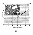
- Figure 1 illustrates a log normal distribution of particles of the invention
- Figure 2 illustrates a device used to prepare filled composites of the invention
- Figure 3 illustrates an electronic package
- the invention provides a filled composite composition, comprising a matrix and a filler composition.
- the filler composition contains particles of a material having a low coefficient of thermal expansion, or CTE.
- the CTE of the particles is 5 ppm/K or less.
- the particles have a negative CTE.
- Filled composite compositions using suitable volume distributions of these characteristic materials can be formulated containing high levels of the filler.
- composites formulated from them can have a net CTE of near or equal to zero. For example, composites with a CTE of 7 ppm/K or less, 5 ppm/K or less, or 3 ppm/K or less may be formulated. In another embodiment, composites with a zero or negative CTE may be formulated.
- the particles of the filler composition are characterized by size distributions exemplified by volume distributions and number distributions.
- the particle volume distribution fv ( D ) gives the fraction of the total filler volume contributed by particles of size D .
- the particle number or count distribution fn ( D ) gives the fraction of the total number of filler particles contributed by particles of size D .
- these two related distributions will have different modes (peak values) and skewnesses.
- the skewnesses and modes of the particle number and volume distributions should be tailored in order to enable higher filler packing densities.
- the filler particle number and volume distributions are tailored in order to achieve high filler packing density.
- the optimal particle distributions depend on particle geometry, fluid (matrix) properties, and particle absolute size range.
- particle distributions are used that are skewed in such a way that the majority of particles are larger than those of the mode.
- the volume distribution mode occurs at a larger value of particle size than the number distribution mode, then most of the filler volume will be contributed by these particles (i.e., those with sizes greater than the number density mode).
- Examples of distributions that can be appropriately tailored toward the desired distributions include non-normal distributions such as log-normal, exponential, power-law, or multi-modal.
- Composites of the invention having CTE near zero are useful in preparing electronic packages and for assembling optical and photonic devices that are subjected to large temperature differences. They serve as underfill, encapsulants, potting materials and the like. They are particular useful in electronic packages containing integrated circuits and optical components made of materials that exhibit very low CTE such as silicon for example. In a preferred embodiment, the CTE of the composites closely matches or is identical with that of the integrated circuit materials.
- Preferred adhesive or encapsulant materials contain matrixes made from such materials as epoxies, polyamides, polyimides, and silicone. These materials generally have fairly large CTE's, on the order of 30-400 ppm/ K. As such, the matrix materials exhibit a large mismatch with typical semiconductor materials used for integrated circuits such as silicon, germanium, gallium arsenide, InP, and InSb, and with typical optical and optical- assembly materials such as quartz and invar.
- Preferred filler materials for the composites of the invention include those having a negative CTE.
- Preferred negative CTE materials are those that exhibit isotropic contraction upon heating. It is also preferred that the contraction upon heating take place over a temperature range that includes ambient conditions.
- Non-limiting examples include ZrVPO 7 , HfVPO 7 and related compounds such as disclosed in U.S. Patent Nos. 5,322,559 and 5,433,778 by Sleight, the disclosures of which are incorporated by reference in their entireties. These materials include compounds that satisfy the general formula A 1-y 4+ A y 1+ A y 3+ V 2-x P x O 7 , where y may vary from about 0 to about 0.4 and more preferably varies from about 0.1 to about 0.2. X may vary from about 0.1 to about 1.9, more preferably from about 0.5 to about 1.5. In a preferred embodiment, x is about 1.
- a 4+ is selected from the group consisting of hafnium, zirconium, Zr a M b , Hf a M b , and mixtures thereof. Generally, the sum of a+b is about 1.
- M is selected from the group consisting of Ti, Ce, Th, U, Mo, Pt, Pb, Sn, Ge, and Si.
- a 1+ represents an alkali metal and A 3+ represents a rare earth metal.
- ZrW 2 O 8 zirconium tungstate
- HfW 2 O 8 hafnium tungstate
- negative CTE materials include blends of compounds M 2 B 3 O 12 having a negative CTE and a second phase of a composition AX 2 O 8 .
- M is selected from the group including aluminum, scandium, indium, yttrium, the lanthanide metals, zirconium and hafnium; B is selected from the group consisting of tungsten, molybdenum and phosphorus; A is zirconium or hafnium; and X is tungsten or molybdenum.
- M is selected from the group including aluminum, scandium, indium, yttrium, the lanthanide metals, zirconium and hafnium
- B is selected from the group consisting of tungsten, molybdenum and phosphorus
- A is zirconium or hafnium
- X is tungsten or molybdenum.
- a filler composition containing particles of the negative CTE material are combined into a matrix.
- a typical CTE is approximately 50 PPM/ K.
- the CTE is approximately -7 ppm/ K.
- the volume fraction is the filler will be given by 1-V m .
- the above formula yields a volume fraction of the matrix of 7/57 and a volume fraction of the filler of 50/57 (0.88). This indicates that, for example, a composite having a net CTE of 0 (zero) may be formulated from such matrix and filler materials if the filler material makes up 88% of the volume of the composite. If the matrix has a CTE of 30 PPM/ K, the same calculation results in a composite having a CTE of about 0 (zero) if the volume fraction of filler particles in the composite is about 30/37 (81%).
- the composite composition comprises at least 62%, preferably 65% or greater by volume filler. In another embodiment, the composition comprises greater than 72%, preferably 75% or greater by volume filler. These volume fractions are generally sufficient to formulate composite compositions having CTE's on the order of 0 to 7 ppm/K for an initial matrix of 30 ppm/K. For matrix materials that have CTEs greater than 30 ppm/K, fill factors into the 80% to 90% range may be required.
- the theoretical maximum volume percent that can be occupied by spherical particles, all of which are the same size, is around 74%.
- mono-size distribution particles, or particles having a normal distribution approaching a mono-size distribution are usually unable to be packed to a volume fraction of greater than about 64% in a composite.
- a wider, appropriately skewed, non-normal, distribution of the negative CTE particles of the invention permits them to be incorporated at levels in the composite higher than that achievable by conventional particles having a normal number distribution.
- the filler particle distribution has a specified maximum particle size which is chosen in order to achieve the desired filler volume within the composite.
- the filler particle number distribution and the volume distribution derived from it should be chosen so that the volume distribution is increasing as the particle size increases while the number distribution is decreasing with increasing particle size.
- the increase of the volume distribution and the decrease of the number distribution are monotonic. Examples of distributions that contain some of these attributes include appropriately shaped log-normal, exponential, power-law, or multi-modal distributions. These are representative distributions that can be shaped to enable higher packing densities than can be achieved with normally-distributed particle sizes.
- One way of preparing non-normal distributions having the above characteristics is to truncate other normal or non-normal distributions.
- such other distributions may be truncated so that only particles with characteristic sizes less than the volume distribution mode are used. In this way, the requirement that the volume distribution decreases with decreasing particle size is satisfied.
- Such truncation may be conveniently carried out by, for example, sieving.
- filler compositions of the invention have a non-normal particle distribution in the sense that, in comparison to a normal distribution, the non-normal distributions of the invention have a relatively greater volume of the particles above the modal size of the distribution than below the modal of the distribution. It is believed that such a distribution provides particles with a wide range of diameters with appropriate number/volume distribution. Such particles may be thought of as roughly spherical in a simple model. In a spherical model, large size particles closely pack leaving interstices between the particles defined by the diameter of the large particle. For efficient packing into a composite, smaller particles are needed that are of sufficient size to fit within interstices defined by larger particles. Of course, in any real world distribution of particles, the simple model will not describe the situation entirely.
- non-normal particle number distributions for use in the invention include, but are not limited to, a log-normal distribution, an exponential distribution, and, in a preferred embodiment, a power-law distribution or a multi-modal distribution.
- the particles have a log normal volume distribution.
- Particles having a log normal volume distribution are characterized in that the logarithm of the particle size is distributed normally about a mean logarithmic particle size.
- Figure 1 illustrates a cumulative log-normal weight (or volume) distribution according to the invention.
- the log of a particle diameter is graphed on the Y axis while a weight percent function is on the X axis.
- the curve in Figure 1 represents the total weight percent of particles in the distribution having a particle size less than or equal to the indicated diameter on the Y axis.
- a graph is linear, as can be seen in Figure 1.
- a plot of the logarithm of cumulative volume against the logarithm of particle size is linear over at least one order of magnitude of particle size, preferably over at least 1.5 orders of magnitude.
- the inset in Figure 1 illustrates the wide range of particle diameters present in such a particle mixture having a log-normal distribution.
- Figure 1 illustrates a further desirable feature of the invention.
- at least 30% by weight of the particles in the filler material is made up of particles with a size less than or equal to about 1 micron ( ⁇ m).
- at least 40%, and more preferably at least 50% of the weight of the particles in the filler composition will be of a diameter less than 1 micron.
- Figure 1 illustrates a particular preferred embodiment where approximately 60% by weight of the particles in the filler composition have a diameter of 1 micron or less.
- this characteristic of a log-normal particle weight (or volume) distribution contributes toward the ability of the composites of the invention to be formed with high loading of filler.
- the invention provides a method for formulating a filled composite having a low, zero, or negative coefficient of thermal expansion, comprising the steps of providing a filler composition and the matrix material, wherein the filler composition comprises particles of a material with a negative CTE and wherein the filler particles have a log-normal or other non-normal particle volume distribution. Thereafter. the composite is made by mixing the filler particles into the matrix.
- the mixing of the filler particles into the matrix may be carried out by conventional means.
- the particular means chosen to mix the filler particles into the matrix will vary depending on the equipment available and the nature of the matrix. In a non-limiting example of formulating filler particles into an epoxy matrix, a mixing procedure is given below.
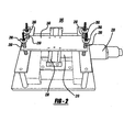
- FIG. 2 illustrates the actuator mixer.
- the mixer 200 consists of a base plate 210 anchored to a linear actuator 220, two rollers 230 attached to a top plate 240, and four spring-loaded posts 250.
- the base plate 210 can be heated to and controlled at a desired temperature.
- the linear actuator 220 when engaged, moves the base plate 210 back and forth at a regular frequency.
- the rollers 230 may be similar to ink rollers and remain stationary during mixing. The rollers are capable of rotating to account for uneven thickness in the sample.
- the rollers and top plate can be pressed against the sample by tightening wing nuts 260 on the four posts 250.
- Mixing is carried out, for example with a device of Figure 2 in order to achieve the best possible dispersion of the negative CTE material, to minimize the formation of voids within the mixture, and to maintain uniform results from mix to mix.
- Example 1 - Zirconium tungstate having a log-normal volume distribution is mixed with an epoxy matrix material to form a composite according to the following procedure.
- Zirconium tungstate having an approximately log normal volume distribution may be purchased from Wah Chang. Part A of an epoxy is placed in a 100 mm wide nylon bag that has been heat sealed on one end. A weighed amount of zirconium tungstate is then placed in the nylon bag. The open end of the bag is then heat sealed, leaving a small amount of air in the bag to aide in mixing.
- the bag is attached to the base plate of the mixer. Before mixing the sample, the base plate is heated to a temperature between 45°C and 50°C. This reduces the viscosity of Part A of the epoxy and aids in the dispersion of the particles.
- the spring-loaded roller plate is now lowered on top of the sample to be mixed and the sleeves are tightened in order to maintain pressure on the sample while mixing.
- the linear actuator is engaged and the sample is allowed to mix for approximately 1 hour. After 1 hour, the mixer is switched off and the sample is removed from the base plate. While the next few steps are performed, the base plate is allowed to cool to room temperature.
- the bag is cut open and the pre-weighed amount of Part B of the epoxy is added to the mixture. It is important to note the time so that the pot life is not exceeded before the mixture is poured into a mold for curing. After Part B is added, the bag is again heat-sealed as before, leaving a small amount of air in the bag.
- the bag is again taped to the base plate of the mixer (which should have cooled to room temperature) and the roller plate is lowered onto the sample as before. Allow the sample to mix for approximately 15 minutes to ensure complete mixing of Part A and Part B. Depending on time constraint and other factors, some samples may be hand mixed at this stage using the nylon trowel.
- the nylon bag is again opened and placed, open end up, in a glass beaker.
- the beaker is then placed in a vacuum oven at room temperature and vacuum is applied. This step removes air bubbles from the mixture and prevents the formation of voids in the sample before, during, and after cure.
- the sample is left in the vacuum oven for approximately 10 minutes, removing the vacuum for 3 seconds every 2-3 minutes to prevent foaming.
- the beaker is removed from the oven and the mixture is now ready for test sample preparation.
- the formulated composite may be used directly to prepare electronic packages.
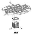
- Example 2 illustrates the invention used to prepare a 3-D electronic device package known as a system in a cube (see Figure 3).
- chips 310 for layering are embedded side by side in an epoxy matrix 320 shaped like a silicon wafer.
- the layers are sliced out of the epoxy wafer and stacked into a module 330.
- Bus metal 340 is deposited on the outside of the stack 330 to bring the I/O from the chips to the cap chip.
- the epoxy matrix 320 contains a low CTE adhesive/encapsulant such as that prepared in Example 1 as a potting compound.
- Example 2 illustrates in part Irvine Sensors' Neo-Stack process as illustrated in IEEE Spectrum, August 2001, pages 46-51.
- an adhesive/encapsulant for assembling and packaging cryo-electronic and super-conductor devices, high power density, solid state and fiber lasers, fiber optic, and power electronic devices, and the like may be formulated by preparing composites made with filler materials having a negative thermal expansion coefficient and logarithmic particle size distribution.
- a class of cubic structure compounds with important isotropic properties has been recently discovered with a large negative thermal expansion coefficient; the compounds are considered suitable for this application.
- the compounds include, without limitation, zirconium tungstate, hafnium tungstate, solid solutions thereof, and their oxides.
- these compounds can be compatibly loaded into polymer resin such as epoxies to high concentrations needed to produce composite materials with expansion properties close to those of electronic and optical components.
- polymer resin such as epoxies
- the large negative CTE property combined with their capability for being highly loaded in matrix resins permits attainment of an adhesive or encapsulant with a CTE of a few or even zero ppm per degree at practically achievable concentrations.
- the filler materials When added and thoroughly dispersed in a polymer resin, the filler materials produce a composite material whose thermal expansion properties can be predicted according to a simple rule of mixtures law. Other materials with more moderate negative expansion coefficients may also be suitable for this application.
- an electronic package according to the invention is capable of operating at temperatures down to 4 K and below without experiencing debonding or delaminating. Because of the close match of the thermal expansion properties of the potting materials/encapsulant to the semiconductor material making up the integrated circuits, such electronic packages are also capable of repeated cycling from high to low temperatures without break down.
- the invention permits use of filled polymer composite adhesives and encapsulants with tailorable CTE properties to assemble and package electronic and optical circuits and passive components made from a wide variety of metal, ceramic, glass and semiconductor materials. Due to the reduced mismatch in CTE between components possible with the materials of this invention, these electronics/photonics elements may be scaled to much larger size, permitting more functionality or capability in the device.
- This scaling feature or capability enabled by the adhesive/encapsulant technology of the invention is important for the development of VLSI superconductor and cryo-electronic integrated technologies. For example, current superconductor IC technology is only at the LSI maturity level.
- the advanced assembly and packaging material of the invention may be used to progress the technology to the VLSI level.
Landscapes
- Physics & Mathematics (AREA)
- Electromagnetism (AREA)
- Engineering & Computer Science (AREA)
- Computer Networks & Wireless Communication (AREA)
- Signal Processing (AREA)
- Structures Or Materials For Encapsulating Or Coating Semiconductor Devices Or Solid State Devices (AREA)
- Compositions Of Macromolecular Compounds (AREA)
Applications Claiming Priority (2)
| Application Number | Priority Date | Filing Date | Title |
|---|---|---|---|
| US425894 | 2003-04-28 | ||
| US10/425,894 US20040214377A1 (en) | 2003-04-28 | 2003-04-28 | Low thermal expansion adhesives and encapsulants for cryogenic and high power density electronic and photonic device assembly and packaging |
Publications (1)
| Publication Number | Publication Date |
|---|---|
| EP1473769A2 true EP1473769A2 (de) | 2004-11-03 |
Family
ID=32990381
Family Applications (1)
| Application Number | Title | Priority Date | Filing Date |
|---|---|---|---|
| EP04009411A Withdrawn EP1473769A2 (de) | 2003-04-28 | 2004-04-21 | Klebstoffe und Einkapselungen mit geringer Wärmeausdehnung zurm Zusammenbau und Verpacken von elektronischen und photonischen Tieftemperatur- und Hochleistungsbauelementen |
Country Status (7)
| Country | Link |
|---|---|
| US (1) | US20040214377A1 (de) |
| EP (1) | EP1473769A2 (de) |
| JP (1) | JP2004327991A (de) |
| KR (1) | KR20040093395A (de) |
| CN (1) | CN1542080A (de) |
| CA (1) | CA2455524A1 (de) |
| TW (1) | TW200422277A (de) |
Cited By (4)
| Publication number | Priority date | Publication date | Assignee | Title |
|---|---|---|---|---|
| WO2008077517A1 (en) * | 2006-12-22 | 2008-07-03 | Sonion Mems A/S | Microphone assembly with underfill agent having a low coefficient of thermal expansion |
| US7632715B2 (en) | 2007-01-05 | 2009-12-15 | Freescale Semiconductor, Inc. | Method of packaging semiconductor devices |
| US8159825B1 (en) | 2006-08-25 | 2012-04-17 | Hypres Inc. | Method for fabrication of electrical contacts to superconducting circuits |
| GB2520511A (en) * | 2013-11-21 | 2015-05-27 | Surf Technology As | Ultrasound transducer |
Families Citing this family (17)
| Publication number | Priority date | Publication date | Assignee | Title |
|---|---|---|---|---|
| US7148577B2 (en) * | 2003-12-31 | 2006-12-12 | Intel Corporation | Materials for electronic devices |
| US7021147B1 (en) | 2005-07-11 | 2006-04-04 | General Electric Company | Sensor package and method |
| DE102006009789B3 (de) * | 2006-03-01 | 2007-10-04 | Infineon Technologies Ag | Verfahren zur Herstellung eines Halbleiterbauteils aus einer Verbundplatte mit Halbleiterchips und Kunststoffgehäusemasse |
| BRPI0808819A2 (pt) * | 2007-03-12 | 2014-08-19 | Koninkl Philips Electronics Nv | Sistema de iluminação e sistema compreendendo o mesmo |
| JP2010021429A (ja) * | 2008-07-11 | 2010-01-28 | Murata Mfg Co Ltd | 電子機器およびその製造方法 |
| TWI629306B (zh) * | 2013-07-19 | 2018-07-11 | Ajinomoto Co., Inc. | Resin composition |
| CN103554844B (zh) * | 2013-10-29 | 2016-02-17 | 广东生益科技股份有限公司 | 一种热固性树脂组合物及其用途 |
| CN107513368B (zh) * | 2017-09-25 | 2020-03-24 | 广州天宸高新材料有限公司 | 耐高温且低膨胀系数的导热灌封胶及其制备方法与应用 |
| CN108336247B (zh) * | 2018-01-30 | 2020-02-07 | 武汉华星光电半导体显示技术有限公司 | 一种oled封装方法及封装结构 |
| US10520679B2 (en) | 2018-06-05 | 2019-12-31 | Globalfoundries Inc. | Fiber alignment to photonics chip |
| JP6484779B1 (ja) * | 2018-07-30 | 2019-03-20 | サンテック株式会社 | 波長可変フィルタ及び光通信機器 |
| JP2020047739A (ja) * | 2018-09-18 | 2020-03-26 | 株式会社東芝 | 超電導コイル、及び、超電導機器 |
| CN112582281B (zh) * | 2019-09-29 | 2023-08-25 | 矽磐微电子(重庆)有限公司 | 半导体封装方法及半导体封装结构 |
| DE102021202222A1 (de) * | 2021-03-08 | 2022-09-08 | Schott Ag | Verbundmaterial |
| KR20250025036A (ko) * | 2022-09-30 | 2025-02-20 | 메이세이 고교 가부시키가이샤 | 발포 수지 단열재 및 그 제조 방법 |
| CN115746781B (zh) * | 2022-11-22 | 2024-04-16 | 黑龙江省科学院石油化学研究院 | 一种改性双马来酰亚胺/氰酸酯胶膜及其制备方法 |
| CN116359086B (zh) * | 2023-06-01 | 2023-09-08 | 南昌科晨电力试验研究有限公司 | 一种基于测量装置的煤粉粒径与质量浓度测量方法 |
Family Cites Families (24)
| Publication number | Priority date | Publication date | Assignee | Title |
|---|---|---|---|---|
| JPH02208256A (ja) * | 1989-02-08 | 1990-08-17 | Denki Kagaku Kogyo Kk | 低熱膨張性セラミックス及びそれを用いた半導体封止材用充填材 |
| JPH0641347A (ja) * | 1992-01-30 | 1994-02-15 | Kyocera Corp | 電子部品封止材用充填材 |
| JPH06200125A (ja) * | 1993-01-06 | 1994-07-19 | Nippon Steel Chem Co Ltd | 半導体封止用低圧トランスファ成形材料 |
| US5322559A (en) * | 1993-05-11 | 1994-06-21 | State Of Oregon Acting By And Through The State Board Of Higher Education On Behalf Of Oregon State University | Negative thermal expansion material |
| US5552092A (en) * | 1994-05-31 | 1996-09-03 | Corning Incorporated | Waveguide coupler |
| US5514360A (en) * | 1995-03-01 | 1996-05-07 | The State Of Oregon, Acting By And Through The Oregon State Board Of Higher Education, Acting For And On Behalf Of Oregon State University | Negative thermal expansion materials |
| US5694503A (en) * | 1996-09-09 | 1997-12-02 | Lucent Technologies Inc. | Article comprising a temperature compensated optical fiber refractive index grating |
| US5919720A (en) * | 1997-04-15 | 1999-07-06 | State Of Oregon Acting By And Through The State Board Of Higher Education On Behalf Of Oregon State University | Materials with low or negative thermal expansion |
| JP2002517377A (ja) * | 1998-05-19 | 2002-06-18 | コーニング インコーポレイテッド | 負の膨張材料、その調製方法および使用方法 |
| US6180241B1 (en) * | 1998-08-18 | 2001-01-30 | Lucent Technologies Inc. | Arrangement for reducing bending stress in an electronics package |
| JP3540628B2 (ja) * | 1998-10-13 | 2004-07-07 | 日東電工株式会社 | 半導体封止用エポキシ樹脂組成物およびそれを用いて得られる半導体装置 |
| US6117704A (en) * | 1999-03-31 | 2000-09-12 | Irvine Sensors Corporation | Stackable layers containing encapsulated chips |
| CN1372531A (zh) * | 2000-03-02 | 2002-10-02 | 日本碍子株式会社 | 沸石成形体、沸石层叠中间体、沸石层叠复合体及其制法 |
| US7192997B2 (en) * | 2001-02-07 | 2007-03-20 | International Business Machines Corporation | Encapsulant composition and electronic package utilizing same |
| JP4155719B2 (ja) * | 2001-02-27 | 2008-09-24 | 電気化学工業株式会社 | 球状無機質粉末及びその用途 |
| WO2003070817A1 (en) * | 2002-02-19 | 2003-08-28 | Photon-X, Inc. | Athermal polymer nanocomposites |
| WO2003079099A1 (en) * | 2002-03-15 | 2003-09-25 | Photon-X, Inc. | Magneto-optic nanocomposites |
| US20030187117A1 (en) * | 2002-03-29 | 2003-10-02 | Starkovich John A. | Materials and method for improving dimensional stability of precision electronic optical photonic and spacecraft components and structures |
| US20030215661A1 (en) * | 2002-05-17 | 2003-11-20 | Jason Lo | Isotropic zero CTE reinforced composite materials |
| US20040063237A1 (en) * | 2002-09-27 | 2004-04-01 | Chang-Han Yun | Fabricating complex micro-electromechanical systems using a dummy handling substrate |
| TW567601B (en) * | 2002-10-18 | 2003-12-21 | Siliconware Precision Industries Co Ltd | Module device of stacked semiconductor package and method for fabricating the same |
| US7023707B2 (en) * | 2003-01-30 | 2006-04-04 | Endicott Interconnect Technologies, Inc. | Information handling system |
| US7811496B2 (en) * | 2003-02-05 | 2010-10-12 | 3M Innovative Properties Company | Methods of making ceramic particles |
| US20040188859A1 (en) * | 2003-03-25 | 2004-09-30 | Intel Corporation | Filler compositions, apparatus, systems, and processes |
-
2003
- 2003-04-28 US US10/425,894 patent/US20040214377A1/en not_active Abandoned
-
2004
- 2004-01-21 CA CA002455524A patent/CA2455524A1/en not_active Abandoned
- 2004-01-30 TW TW093102238A patent/TW200422277A/zh unknown
- 2004-02-10 CN CNA2004100042068A patent/CN1542080A/zh active Pending
- 2004-04-01 KR KR1020040022482A patent/KR20040093395A/ko not_active Withdrawn
- 2004-04-19 JP JP2004122758A patent/JP2004327991A/ja active Pending
- 2004-04-21 EP EP04009411A patent/EP1473769A2/de not_active Withdrawn
Cited By (7)
| Publication number | Priority date | Publication date | Assignee | Title |
|---|---|---|---|---|
| US8159825B1 (en) | 2006-08-25 | 2012-04-17 | Hypres Inc. | Method for fabrication of electrical contacts to superconducting circuits |
| US9647194B1 (en) | 2006-08-25 | 2017-05-09 | Hypres, Inc. | Superconductive multi-chip module for high speed digital circuits |
| US10373928B1 (en) | 2006-08-25 | 2019-08-06 | Hypres, Inc. | Method for electrically interconnecting at least two substrates and multichip module |
| WO2008077517A1 (en) * | 2006-12-22 | 2008-07-03 | Sonion Mems A/S | Microphone assembly with underfill agent having a low coefficient of thermal expansion |
| US8189820B2 (en) | 2006-12-22 | 2012-05-29 | Sonion Mems A/S | Microphone assembly with underfill agent having a low coefficient of thermal expansion |
| US7632715B2 (en) | 2007-01-05 | 2009-12-15 | Freescale Semiconductor, Inc. | Method of packaging semiconductor devices |
| GB2520511A (en) * | 2013-11-21 | 2015-05-27 | Surf Technology As | Ultrasound transducer |
Also Published As
| Publication number | Publication date |
|---|---|
| CN1542080A (zh) | 2004-11-03 |
| CA2455524A1 (en) | 2004-10-28 |
| TW200422277A (en) | 2004-11-01 |
| US20040214377A1 (en) | 2004-10-28 |
| JP2004327991A (ja) | 2004-11-18 |
| KR20040093395A (ko) | 2004-11-05 |
Similar Documents
| Publication | Publication Date | Title |
|---|---|---|
| EP1473769A2 (de) | Klebstoffe und Einkapselungen mit geringer Wärmeausdehnung zurm Zusammenbau und Verpacken von elektronischen und photonischen Tieftemperatur- und Hochleistungsbauelementen | |
| Licari et al. | Adhesives technology for electronic applications: materials, processing, reliability | |
| AU651461B2 (en) | Semiconductor chip module | |
| US20110135015A1 (en) | Cooling devices in semiconductor packages | |
| EP0665591A1 (de) | Verfahren zur herstellung einer Verpackung für Leistungsschaltungen | |
| KR20060086937A (ko) | 도전성 나노입자를 이용한 열전도성 물질 | |
| Wang et al. | Encapsulant for fatigue life enhancement of controlled-collapse chip connection (C4) | |
| US6238954B1 (en) | COF packaged semiconductor | |
| EP0379773A1 (de) | Diamantgefüllter Epoxidharzklebstoff mit thermischer Leitfähigkeit und elektrischem Widerstand | |
| JP3121020B2 (ja) | 半導体装置の製法およびそれに用いる封止用ペレット | |
| EP2760044A1 (de) | Eingebettete Verpackung auf Verpackungssystemen | |
| JPWO1996027900A1 (ja) | 半導体装置の製法およびそれに用いる封止用ペレット | |
| EP3332419B1 (de) | Flip-chip-modul mit verbesserten eigenschaften | |
| Xu et al. | Effects of the low loss polymers on the dielectric behavior of novel aluminum-filled high-k nano-composites | |
| Vertyanov et al. | Effects of multilayer structures made of epoxy compounds with different filler contents on thermo-mechanical stresses in 3D packages | |
| Thomas et al. | Packaging Platform for low to medium Power Packages | |
| Colonna et al. | Thermal and Mechanical Simulations for Fan-Out Wafer-Level Packaging Technology: Introduction of a" Solder Heatsink" | |
| Hokanson et al. | A shear-based optimization of adhesive thickness for die bonding | |
| Dietz et al. | New high thermal conductivity thermoplastics for power applications | |
| Matsumoto et al. | Thermal performance evaluation of dual-side cooling for a three-dimensional (3D) chip stack: Additional cooling from the laminate (substrate) side | |
| US20250079258A1 (en) | Package structures for efficient heat dissipation | |
| Wong et al. | Mixed filler combinations for enhanced thermal conductivity of liquid encapsulants for electronic packaging | |
| US20250304830A1 (en) | One-part dispensables and methods for reducing the spreading of material(s) migrating from one-part dispensables and/or for improving vertical stability of one-part dispensables | |
| JPH09260432A (ja) | 半導体装置の製法 | |
| Su et al. | Research on controllable heat dissipation of system in ceramic package |
Legal Events
| Date | Code | Title | Description |
|---|---|---|---|
| PUAI | Public reference made under article 153(3) epc to a published international application that has entered the european phase |
Free format text: ORIGINAL CODE: 0009012 |
|
| AK | Designated contracting states |
Kind code of ref document: A2 Designated state(s): AT BE BG CH CY CZ DE DK EE ES FI FR GB GR HU IE IT LI LU MC NL PL PT RO SE SI SK TR |
|
| AX | Request for extension of the european patent |
Extension state: AL HR LT LV MK |
|
| STAA | Information on the status of an ep patent application or granted ep patent |
Free format text: STATUS: THE APPLICATION HAS BEEN WITHDRAWN |
|
| 18W | Application withdrawn |
Effective date: 20080611 |