EP1471702B1 - CMOS-Leitungstreiberschaltung mit einstellbarer Ausgangsimpedanz - Google Patents
CMOS-Leitungstreiberschaltung mit einstellbarer Ausgangsimpedanz Download PDFInfo
- Publication number
- EP1471702B1 EP1471702B1 EP04009316A EP04009316A EP1471702B1 EP 1471702 B1 EP1471702 B1 EP 1471702B1 EP 04009316 A EP04009316 A EP 04009316A EP 04009316 A EP04009316 A EP 04009316A EP 1471702 B1 EP1471702 B1 EP 1471702B1
- Authority
- EP
- European Patent Office
- Prior art keywords
- driver
- output
- von
- impedance
- positive
- Prior art date
- Legal status (The legal status is an assumption and is not a legal conclusion. Google has not performed a legal analysis and makes no representation as to the accuracy of the status listed.)
- Expired - Lifetime
Links
Images





Classifications
-
- H—ELECTRICITY
- H04—ELECTRIC COMMUNICATION TECHNIQUE
- H04L—TRANSMISSION OF DIGITAL INFORMATION, e.g. TELEGRAPHIC COMMUNICATION
- H04L25/00—Baseband systems
- H04L25/02—Details ; arrangements for supplying electrical power along data transmission lines
- H04L25/0264—Arrangements for coupling to transmission lines
- H04L25/0278—Arrangements for impedance matching
-
- H—ELECTRICITY
- H03—ELECTRONIC CIRCUITRY
- H03K—PULSE TECHNIQUE
- H03K19/00—Logic circuits, i.e. having at least two inputs acting on one output; Inverting circuits
- H03K19/0005—Modifications of input or output impedance
-
- H—ELECTRICITY
- H04—ELECTRIC COMMUNICATION TECHNIQUE
- H04L—TRANSMISSION OF DIGITAL INFORMATION, e.g. TELEGRAPHIC COMMUNICATION
- H04L25/00—Baseband systems
- H04L25/02—Details ; arrangements for supplying electrical power along data transmission lines
- H04L25/0264—Arrangements for coupling to transmission lines
- H04L25/0272—Arrangements for coupling to multiple lines, e.g. for differential transmission
-
- H—ELECTRICITY
- H04—ELECTRIC COMMUNICATION TECHNIQUE
- H04L—TRANSMISSION OF DIGITAL INFORMATION, e.g. TELEGRAPHIC COMMUNICATION
- H04L25/00—Baseband systems
- H04L25/02—Details ; arrangements for supplying electrical power along data transmission lines
- H04L25/0264—Arrangements for coupling to transmission lines
- H04L25/028—Arrangements specific to the transmitter end
-
- H—ELECTRICITY
- H04—ELECTRIC COMMUNICATION TECHNIQUE
- H04L—TRANSMISSION OF DIGITAL INFORMATION, e.g. TELEGRAPHIC COMMUNICATION
- H04L25/00—Baseband systems
- H04L25/02—Details ; arrangements for supplying electrical power along data transmission lines
- H04L25/08—Modifications for reducing interference; Modifications for reducing effects due to line faults ; Receiver end arrangements for detecting or overcoming line faults
- H04L25/085—Arrangements for reducing interference in line transmission systems, e.g. by differential transmission
Definitions
- the present invention relates to line drivers, and more particularly, to differential line drivers with impedance that is matched to the line.
- drivers with output impedance matched to the line impedance are used.
- a conventional voltage mode series terminated driver can be realized using an inverter with proper sizing of the NMOS and PMOS transistors to give an output impedance equal to the line impedance, which is typically 50 ohms.
- a circuit implementation of such a driver 100 in its differential form is shown in FIG. 1 .
- PMOS transistors MP1, MP2 and NMOS transistors MN1, MN2 are sized to give a nominal output impedance of 50 ohms to drive a 50 ohm line.
- the output impedance of the transmit driver be closely matched to the characteristic impedance of the line, typically within 10% or better.
- the turn-on resistance of the NMOS or PMOS transistors may vary by 50% or more across process, supply voltage and temperature variations.
- the driver 100 of FIG. 1 can be improved if the output impedance is made up of the sum of the resistance of a transistor switch and a resistor R1 as shown in FIG. 2 .
- the output impedance of the driver 200 of FIG. 2 can be made to be dominated by the resistor R1, especially since the variation of a resistor across process, voltage and temperature variation is usually much less than that of a transistor. However, the variation is often still in the order of 20 to 30%. Achieving adequate output impedance matching requires some form of calibration or compensation mechanism. As shown in FIG. 3 and FIG. 4 , this can be done by digitally trimming the resistance value if the driver 100 of FIG. 1 or the driver 200 of FIG. 2 is replaced by a segmented driver where segments are switched in or out by control lines ctlp0...ctlpi and cltn0... ctlni to match the output impedance of the driver to the impedance of the line as closely as possible.
- FIG. 3 shows a segmented driver using the driver cell structure 100 of FIG. 1
- FIG. 4 shows a segmented driver using the driver cell structure 200 of FIG. 2
- each segment of the driver is enabled only if ctlpi and ctlni is asserted high. For example if ctlp1 and ctln1 are asserted high, then transistors MP1 and MN1 are enabled to invert the input signal Vip. This corresponds to reducing the output impedance, since the turn-on resistances of MP1 and MN1 are added in parallel with the existing driver total output impedance.
- control lines ctlp and ctln are usually driven by a feedback control circuit that compares the output impedance of a replica output driver with that of an external reference resistor. After each comparison, a finite state machine uses the control lines ctlp and ctln to turn on or off driver segments to adjust the total driver output impedance to match and track the impedance of an external reference resistor.
- the signal (Vip, Vin) and control (ctlp, ctln) shares the same logic path through the logic gates.
- the logic gates in each driver segment introduce additional delay mismatches between the PMOS and NMOS transistor inputs, since the logic required to turn off an NMOS transistor is different from that for a PMOS transistor. This has the effect of shining signal transitions away from the desired voltage point. Even if the logic were to be made similar, the loading for the output of the logic circuits would be different, since typically PMOS transistors are larger than NMOS transistors, and this can cause additional delay variation and mismatches.
- both PMOS and NMOS transistors can be turned on. This causes a large transient shoot through current given by V DD /(Resistance of PMOS transistor + Resistance of NMOS transistor) at that instant.
- FIG. 5 A calibration circuit that can be used to calibrate the segmented driver is shown in FIG. 5 .
- FIG. 5 shows the one half of the circuit required to perform impedance calibration for the segmented driver of FIG. 4 .
- the circuit in FIG. 5 uses a replica of the PMOS side of the segmented driver (see William J. Dally and John W. Poulton," Digital Systems Engineering” Cambridge University Press, pp. 519-521 ).
- the principle of operation of the circuit of FIG. 5 is as follows: an external resistor R EXT and a current source 501 is used to generate a voltage reference at node V1.
- a matched current source 502 sinks current from the PMOS side of a replica segmented driver. The voltage drop across the PMOS side output impedance will determine the voltage at V2 .
- the state machine will then turn on each driver segment by asserting ctlp0 to ctlpi. As each segment is turned on, the voltage at V2 is compared to that at V1. When a transition is detected, this indicates that the voltage at V1 is nearly equal to that of V1.
- the output resistance of the PMOS side is thus matched to that of the external resistor R EXT .
- the reference current source needs the same amount of current as the current that flows through the 50 ohm output driver. This current is significant, and is an inefficient use of available current.
- the reference current source can be made smaller and the reference resistor larger, but this introduces greater matching and scaling errors.
- US 6,351,185 describes a line driver and a method for increasing available signal transmit power on a transmission line.
- the line driver achieves an available transmit power increase without increasing the maximum current in the line driver output stage.
- the output stage of the line driver may comprise a first amplifier, a second amplifier, and an integrated back-matching resistor network.
- a protective semiconductor device may be added to a line driver output stage for each semiconductor device in the first and second amplifiers.
- EP 0 969 633 refers to a driver circuit unit comprising a first push pull circuit for issuing an output signal to an output terminal through resistors when transmitted data is issued to an input terminal, the output signal having its logic level correspond to the transmitted data; a second push pull circuit for issuing al negative-phase output signal to a further output terminal through further resistors when negative-phase data, which is one reversed in phase of the above transmitted data, is issued to a further input terminal, the negative-phase output signal having its logic level correspond to the negative-phase data; and, a resistor connected between the output terminal and the further output terminal.
- FIG. 1 shows a conventional differential line driver cell.
- FIG. 2 shows a modified conventional differential line driver cell.
- FIG. 3 shows a plurality of conventional driver cells of FIG. 1 arranged in parallel.
- FIG. 4 shows a plurality of conventional driver cells of FIG. 2 arranged in parallel.
- FIG. 5 shows a conventional differential line driver calibration circuit.
- FIG. 6 shows a differential line driver cell used in the present invention.
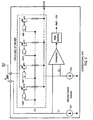
- FIG. 7 shows a calibration circuit for the differential line driver cell of the present invention.
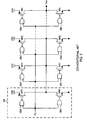
- FIG. 8 shows a number of half cells of the present invention arranged in parallel.
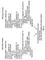
- FIG. 9 illustrates the calibration process used in the driver of FIGs. 7 and 8 .
- the proposed invention overcomes the disadvantages outlined for both the driver structure of FIG. 2 , the segmented structure of FIG. 4 , its associated calibration circuitry of FIG. 5 and the similar scheme described in Gabara et al.
- the output impedance of prior art inverter type drivers as shown in FIG. 1 changes significantly with the output voltage.
- the resistors and transistors are sized such that the resistors provide the dominant termination impedance, then the output impedance of the driver will vary insignificantly with respect to the output voltage.
- the transient shoot through current is reduced compared to the conventional inverter type series termination type drivers.
- An output driver normally includes a number N of driver cells, or segments.
- the number of driver cells switched on (or enabled) is determined by the impedance calibration circuitry.
- the calibration circuitry can use comparators, a state machine and feedback loop to switch on or off the required number of driver cells, to match and track the impedance of an external resistor.
- FIG. 6 shows a diagram of a single driver cell 600 such a cell is known from EP 0 969 633 A2 .
- the driver cell 600 that is enabled by ctlp and ctln that control series PMOS and NMOS switches is shown.
- the differential line driver cell 600 of the present invention includes a switch, for example, a PMOS transistor MP3 driven by a control signal ctlp.
- the transistor MP3 is connected to sources of two PMOS transistors MP1 and MP2. Drains of the transistors MP1 and MP2 are connected to resistors RP1 and RP2, respectively, which are in turn connected to resistors RN1 and RN2, respectively.
- the transistors RN1 and RN2 are connected to two NMOS transistors MN1 and MN2, whose sources are tied together and to a second switch (for example, an NMOS transistor NM3) that is controlled by a negative control signal ctln.
- FIG. 7 shows a diagram of the calibration circuit of the present invention.
- an impedance switchable driver D1 typically comprises a plurality of driver cells 600, one of which is illustrated in FIG. 6 .
- the PMOS side and the NMOS side both have their own calibration feedback loops.
- One of the feedback loops includes a comparator C1, and a state machine L1 that outputs control signals ctlp0 ... ctlpi.
- the NMOS branch includes a comparator C2 and a state machine L2 that outputs the control signals ctln0...ctlni.
- a reference ladder may be used to generate reference voltages VR1 and VR2 for use by the comparators C1 and C2.
- the circuit is therefore essentially a dual closed loop system that forces Vop to track VR1 and Von to track VR2. When Vop is equal to VR1 and Von is equal to VR2 then the driver output impedance will be 50 ohms on each side.
- the driver cell 600 of FIG. 6 When ctlp is asserted low to 0 volts and ctln is asserted high to the supply voltage, the driver cell 600 of FIG. 6 is enabled. Assuming Vip is pulled low, and Vin pulled high, the output impedance of the driver of FIG. 7 at Von is given by the sum of the impedances of transistors MP3, MP1 and resistor Rp1. The output impedance at Vop is given by the sum of the impedances R(MN3), R(MN2) of transistors MN3, MN2, respectively and resistor Rn2 .
- Transistors MP3 and MP1 are sized such that their impedances, R(MP3), R(MP1), when combined, are less than 10% of R(Von ). This provides a relatively small voltage drop across the transistors MP3 and MP1, keeping them in a linear region during the time when they are turned on. In the linear region, the transistors behave like a linear resistor. By keeping the transistors MP3 and MP1 in the linear region, R (Von) can be made to be independent of output voltage at Von.
- FIG. 8 shows the segmented driver D1 in additional detail, showing the overall arrangement of the driver cells 600 of FIG. 6 . Note that only one side (the PMOS side) of the segmented driver D1 is shown, to make the diagram simpler.
- the outputs of all the driver cells 600 are shorted together at Vop, Von , such that the total output impedance of the segmented driver is R( Von )/N, where N is the number of driver cells 600 (assuming all N driver cells 600 are enabled).
- the input signal Vip is shorted to the input of all driver cells 600 , ensuring that each driver cell 600 sees substantially the same input signal and loading conditions.
- the segmented driver structure D1 of FIG. 8 is calibrated by connecting it's outputs to an accurate external reference resistor R EXT (see FIG. 7 ) and placing it in a feedback loop such that the output impedance of the driver D1 will track the impedance of the reference resistor.
- the accuracy of the impedance calibration is determined by the number N of driver cells 600 covering an impedance range and by the coupling factor between Von and Vop .
- N the number of driver cells currently switched on.
- the minimum voltage step is 1.56 x Iout, where Iout is the current flowing through the driver and is given by V DD /200 amps.
- K is the coupling coefficient
- ⁇ Von represents an incremental change in Von
- ⁇ Vop represents an incremental change in Vop .
- the impedance of the NMOS branch is R( Von )/32 and of the PMOS branch is R( Vop )/32 .
- the comparators C1 and C2 then compare Vop with VR1 and Von with VR2, respectively. If Vop is greater than VR2, this corresponds to R( Von ) being greater than the required impedance value.
- This the algorithm will increase the number of turned on NMOS branches in driver cells 600.
- the number of cells 600 turned on for the NMOS branch, referred to as Nn here, is stored in a register.
- This process of comparing and incrementing or decrementing Nn value is repeated another seven times, with each Nn value summed or accumulated with the previous Nn values. This is denoted as steps 4 to 6 in FIG. 9 .
- each averaged Nn value is compared with its previous averaged Nn value. If they are equal, this means that the average of the current eight Nn values and the average of the previous eight Nn values are equal, and therefore the impedance value has converged to a stable value.
- the algorithm then outputs the corresponding averaged Nn value to set the impedance of the driver. Exactly the same process occurs for the PMOS branch. When both NMOS and PMOS branches have converged to their respective impedance values, the calibration clock is stopped and the logic signals that calibration has completed.
- the proposed calibration circuitry has a number of advantages over conventional art. It is much more area efficient compared to the conventional art circuit as shown in FIG. 5 due to the following reasons:
- Matched current sources 501 and 502 of FIG. 5 are not needed and this saves significant area because these current sources that are connected directly to or indirectly through the PMOS branch to a bonding pad, require special layout rules for ESD protection. This would typically increase the area required for the current sources to 5 to 10 times their normal area.
- only one external reference resistor is needed to calibrate both NMOS and PMOS branches for the invention compared to two resistors required for the prior art of FIG. 5 .
- the calibration circuit proposed by Gabara et al. uses only one reference resistor as well, but introduces an additional calibrated NMOS branch (i.e., bottom half of driver) to act as a reference resistor to calibrate the PMOS branch (i.e., upper half of driver).
- the present invention does not require an additional reference resistor nor an additional NMOS or PMOS branch, and hence results in smaller area.
- the proposed driver can be used as a replica for calibration "as is.”
- the calibration circuit described herein also is more current efficient than the implementation as shown in FIG. 5 and as described in Gabara et al. and Dally et al. This is due to the fact that the reference resistor is configured as the actual resistance load of the output driver. This enables the current that flows through the driver to flow through the reference resistor as well, unlike the conventional circuit of FIG. 5 , which requires additional current to flow through the external reference resistor to generate a reference voltage. In addition, two reference voltage generators and four times the amount of current is needed to calibrate the upper and bottom half of the driver for the scheme described in Gabara et al.
- the driver cell structure 600 of the present invention also has a number of advantages over conventional art.
- Conventional inverter drivers share the same signal and control path.
- the signal path and the control path are separated, allowing the removal of any control logic from the signal path. This improves signal delay and slope variation at the input of different driver cells, and also at the input of the NMOS and PMOS switches.
- the transient shoot through current is reduced compared to the conventional inverter type series termination type drivers. This is due to the fact that the termination resistors are in series with the transistor switches. Therefore when both PMOS and NMOS switches are on, the transient shoot through current, which is given by V DD divided by a larger resistance, is reduced.
Landscapes
- Engineering & Computer Science (AREA)
- Power Engineering (AREA)
- Computer Networks & Wireless Communication (AREA)
- Signal Processing (AREA)
- Physics & Mathematics (AREA)
- Computer Hardware Design (AREA)
- Computing Systems (AREA)
- General Engineering & Computer Science (AREA)
- Mathematical Physics (AREA)
- Logic Circuits (AREA)
Claims (6)
- Differential-Leitungstreiber mit:einer Vielzahl von Treiberzellen, die einen gemeinsamen Eingang (Vip) als einen positiven Eingang und einen gemeinsamen Eingang (Vin) als einen negativen Eingang und einen gemeinsamen Ausgang (Vop) als einen positiven Ausgang und einen gemeinsamen Ausgang (Von) als einen negativen Ausgang für das Ansteuern einer Leitung aufweisen; undeiner Steuerlogik, die positive und negative Steuersignale für die Treiberzellen erzeugt, um so eine kombinierte Ausgangsimpedanz der Treiberzellen an (Vop, Von) an die Leitung anzupassen;wobei jede Treiberzelle Folgendes umfasst:einen ersten PMOS-Transistor (MP1) und einen ersten NMOS-Transistor (MN1), die Gates aufweisen, die von dem Eingang (Vip) angesteuert werden;einen zweiten PMOS-Transistor (MP2) und einen zweiten NMOS-Transistor (MN2), die Gates aufweisen, die von dem Eingang Vin angesteuert werden, wobei eine Source des ersten PMOS-Transistors (MP1) mit einer Source des zweiten PMOS-Transistors (MP2) verbunden ist, und wobei eine Source des ersten NMOS-Transistors (MN1) mit einer Source des zweiten NMOS-Transistors (MN2) verbunden ist;erste und zweite Widerstände (Rp1, Rn1), die zwischen dem ersten PMOS-Transistor (MP1) und dem ersten NMOS-Transistor (MN1) in Reihe geschaltet sind und an dem Ausgang (Von) miteinander verbunden sind;dritte und vierte Widerstände (Rp2, Rn2), die zwischen dem zweiten PMOS-Transistor (MP2) und dem zweiten NMOS-Transistor (MN2) in Reihe geschaltet sind und an dem Ausgang (Vop) miteinander verbunden sind;einen ersten Ausgangsschalter (MP3), der von einem entsprechenden positiven Steuersignal (ctlp) angesteuert wird und zwischen einer Versorgungsspannung und den Sources der ersten und zweiten PMOS-Transistoren geschaltet ist; undeinen zweiten Ausgangsschalter (MN3), der von einem entsprechenden negativen Steuersignal (ctln) angesteuert wird und zwischen einer Masse und den Sources der ersten und zweiten PMOS-Transistoren geschaltet ist.
- Differential-Leitungstreiber nach Anspruch 1, der des Weiteren einen externen Widerstand umfasst, der zwischen die Ausgänge (Vop, Von) geschaltet ist.
- Differential-Leitungstreiber nach Anspruch 1, wobei die Steuerlogik eine Zustandsmaschine umfasst.
- Differential-Leitungstreiber nach Anspruch 1, der des Weiteren eine Rückkopplungsschleife zum Steuern der Treiberzellen mit selektiven positiven und negativen Steuersignalen zu ausgewählten Treiberzellen umfasst, um so eine kombinierte Ausgangsimpedanz der Treiberzellen anzupassen.
- Differential-Leitungstreiber nach Anspruch 4, der des Weiteren einen externen Widerstand umfasst, der zwischen den positiven Ausgang und den negativen Ausgang geschaltet ist.
- Differential-Leitungstreiber nach Anspruch 1, wobei ein Signalweg für die positiven und negativen Eingänge anders als ein Signalweg für die positiven und negativen Steuersignale ist.
Applications Claiming Priority (2)
| Application Number | Priority Date | Filing Date | Title |
|---|---|---|---|
| US10/419,886 US6771097B1 (en) | 2003-04-22 | 2003-04-22 | Series terminated CMOS output driver with impedance calibration |
| US419886 | 2003-04-22 |
Publications (2)
| Publication Number | Publication Date |
|---|---|
| EP1471702A1 EP1471702A1 (de) | 2004-10-27 |
| EP1471702B1 true EP1471702B1 (de) | 2008-06-25 |
Family
ID=32771707
Family Applications (1)
| Application Number | Title | Priority Date | Filing Date |
|---|---|---|---|
| EP04009316A Expired - Lifetime EP1471702B1 (de) | 2003-04-22 | 2004-04-20 | CMOS-Leitungstreiberschaltung mit einstellbarer Ausgangsimpedanz |
Country Status (3)
| Country | Link |
|---|---|
| US (3) | US6771097B1 (de) |
| EP (1) | EP1471702B1 (de) |
| DE (1) | DE602004014559D1 (de) |
Families Citing this family (39)
| Publication number | Priority date | Publication date | Assignee | Title |
|---|---|---|---|---|
| US6771097B1 (en) * | 2003-04-22 | 2004-08-03 | Broadcom Corporation | Series terminated CMOS output driver with impedance calibration |
| US7221196B2 (en) * | 2003-12-05 | 2007-05-22 | Aquantia Corporation | Low-power low-voltage multi-level variable-resistor line driver |
| KR100549869B1 (ko) * | 2004-10-18 | 2006-02-06 | 삼성전자주식회사 | 의사 차동 출력 버퍼, 이를 이용한 메모리 칩 및 메모리시스템 |
| US7528629B2 (en) * | 2004-11-18 | 2009-05-05 | Aquantia Corporation | Low-power low-voltage multi-level variable-resistor line driver |
| US7532048B1 (en) | 2004-11-18 | 2009-05-12 | Aquantia Corporation | Multi-level variable-resistor line driver |
| US7352204B2 (en) * | 2005-05-13 | 2008-04-01 | Warpspeed Chips, Llc | Automatic skew correction for differential signals |
| ITMI20051276A1 (it) * | 2005-07-06 | 2007-01-07 | St Microelectronics Srl | Trasmettitore multi-standard |
| US7389194B2 (en) | 2005-07-06 | 2008-06-17 | Rambus Inc. | Driver calibration methods and circuits |
| JP2007036848A (ja) * | 2005-07-28 | 2007-02-08 | Ricoh Co Ltd | ドライバ回路 |
| US7307447B2 (en) * | 2005-10-27 | 2007-12-11 | International Business Machines Corporation | Self series terminated serial link transmitter having segmentation for amplitude, pre-emphasis, and slew rate control and voltage regulation for amplitude accuracy and high voltage protection |
| US7312629B2 (en) * | 2006-05-17 | 2007-12-25 | Sony Corporation | Programmable impedance control circuit calibrated at Voh, Vol level |
| US7501851B2 (en) * | 2006-05-26 | 2009-03-10 | Pmc Sierra Inc. | Configurable voltage mode transmitted architecture with common-mode adjustment and novel pre-emphasis |
| US7913199B2 (en) * | 2006-07-14 | 2011-03-22 | International Business Machines Corporation | Structure for a duty cycle correction circuit |
| US7417480B2 (en) * | 2006-07-14 | 2008-08-26 | International Business Machines Corporation | Duty cycle correction circuit whose operation is largely independent of operating voltage and process |
| US20080018357A1 (en) * | 2006-07-18 | 2008-01-24 | Honeywell International Inc. | Automatic termination circuit |
| US7459930B2 (en) * | 2006-11-14 | 2008-12-02 | Micron Technology, Inc. | Digital calibration circuits, devices and systems including same, and methods of operation |
| US7579876B1 (en) * | 2007-01-17 | 2009-08-25 | Scintera Networks, Inc. | Multi-use input/output pin systems and methods |
| US20090128206A1 (en) * | 2007-11-20 | 2009-05-21 | Boerstler David W | Apparatus and Method for Obtaining Desired Phase Locked Loop Duty Cycle without Pre-Scaler |
| US8108813B2 (en) * | 2007-11-20 | 2012-01-31 | International Business Machines Corporation | Structure for a circuit obtaining desired phase locked loop duty cycle without pre-scaler |
| US8381143B2 (en) * | 2008-05-29 | 2013-02-19 | International Business Machines Corporation | Structure for a duty cycle correction circuit |
| CN102396156A (zh) | 2009-02-12 | 2012-03-28 | 莫塞德技术公司 | 用于片内终结的终结电路 |
| KR101605463B1 (ko) * | 2009-03-04 | 2016-03-22 | 삼성전자 주식회사 | 피브이티 변동에 둔감한 딜레이 라인을 갖는 지연 고정 루프회로 |
| US7868668B2 (en) * | 2009-05-13 | 2011-01-11 | Faraday Technology Corp. | Power-on detector and method thereof |
| US7893720B2 (en) * | 2009-07-18 | 2011-02-22 | Texas Instruments Incorporated | Bus low voltage differential signaling (BLVDS) circuit |
| US8624641B1 (en) * | 2010-11-03 | 2014-01-07 | Pmc-Sierra, Inc. | Apparatus and method for driving a transistor |
| US8760189B2 (en) * | 2011-09-29 | 2014-06-24 | Qualcomm Incorporated | Apparatus to implement symmetric single-ended termination in differential voltage-mode drivers |
| JP5447575B2 (ja) * | 2012-04-23 | 2014-03-19 | 株式会社デンソー | 駆動装置 |
| FR2991501A1 (fr) | 2012-05-30 | 2013-12-06 | Stmicroelectronic Sa | Circuit integre comportant au moins un port digital de sortie d'impedance reglable, et procede de reglage correspondant |
| US9083330B2 (en) * | 2013-10-17 | 2015-07-14 | Qualcomm Incorporated | Output driver with slew rate calibration |
| US9166565B2 (en) * | 2013-10-17 | 2015-10-20 | Qualcomm Incorporated | Calibrated output driver with enhanced reliability and density |
| US9510232B2 (en) | 2014-07-09 | 2016-11-29 | T-Mobile Usa, Inc. | Cellular network backhaul oversubscription |
| US9455713B1 (en) | 2015-06-02 | 2016-09-27 | Avago Tcehnologies General IP (Singapore) Pte. Ltd. | Split resistor source-series terminated driver |
| JP6807642B2 (ja) | 2016-01-08 | 2021-01-06 | ザインエレクトロニクス株式会社 | 送信装置 |
| EP3373526B1 (de) * | 2017-03-07 | 2020-01-08 | Nxp B.V. | Sender mit unabhängig einstellbarer spannung und impedanz |
| US10897250B2 (en) * | 2018-11-16 | 2021-01-19 | Transportation Ip Holdings, Llc | Systems and methods for controlling dynamic avalanche in switching devices |
| CN112737562B (zh) * | 2020-12-24 | 2025-01-21 | 西安翔腾微电子科技有限公司 | 一种带有阻抗校正电路的高速电压模发送器 |
| US12063033B2 (en) * | 2021-07-30 | 2024-08-13 | Renesas Electronics America Inc. | Apparatus for multi-driver architecture with high voltage protection and impedance control |
| US12567845B2 (en) * | 2022-01-10 | 2026-03-03 | Samsung Electronics Co., Ltd. | Amplifier and electronic system including the same |
| JP2023146812A (ja) * | 2022-03-29 | 2023-10-12 | ラピステクノロジー株式会社 | 出力回路 |
Family Cites Families (10)
| Publication number | Priority date | Publication date | Assignee | Title |
|---|---|---|---|---|
| US4992676A (en) * | 1989-05-01 | 1991-02-12 | Motorola, Inc. | Output buffer having distributed stages to reduce switching noise |
| DE69231920T2 (de) * | 1991-12-17 | 2002-04-11 | Stmicroelectronics, Inc. | Ausgangspufferschaltung mit Vorladung |
| JPH0669770A (ja) | 1992-08-14 | 1994-03-11 | Nec Ic Microcomput Syst Ltd | 遅延回路 |
| GB2305082B (en) * | 1995-09-06 | 1999-10-06 | At & T Corp | Wave shaping transmit circuit |
| DE19646684C1 (de) * | 1996-11-12 | 1998-03-05 | Ericsson Telefon Ab L M | Ausgangspufferschaltkreis |
| JP2000022516A (ja) * | 1998-06-30 | 2000-01-21 | Nec Corp | ドライバ回路装置 |
| US6133749A (en) * | 1999-01-04 | 2000-10-17 | International Business Machines Corporation | Variable impedance output driver circuit using analog biases to match driver output impedance to load input impedance |
| US6351185B1 (en) * | 1999-08-16 | 2002-02-26 | Globespan, Inc. | Increased output swing line drivers for operation at supply voltages that exceed the breakdown voltage of the integrated circuit technology |
| US6704818B1 (en) * | 2000-12-29 | 2004-03-09 | Intel Corporation | Voltage-mode driver with pre-emphasis, slew-rate control and source termination |
| US6771097B1 (en) * | 2003-04-22 | 2004-08-03 | Broadcom Corporation | Series terminated CMOS output driver with impedance calibration |
-
2003
- 2003-04-22 US US10/419,886 patent/US6771097B1/en not_active Expired - Fee Related
-
2004
- 2004-04-20 EP EP04009316A patent/EP1471702B1/de not_active Expired - Lifetime
- 2004-04-20 DE DE602004014559T patent/DE602004014559D1/de not_active Expired - Lifetime
- 2004-06-08 US US10/862,467 patent/US6894543B2/en not_active Expired - Fee Related
-
2005
- 2005-01-28 US US11/044,177 patent/US7078943B2/en not_active Expired - Fee Related
Also Published As
| Publication number | Publication date |
|---|---|
| US20040222821A1 (en) | 2004-11-11 |
| US7078943B2 (en) | 2006-07-18 |
| US20050127958A1 (en) | 2005-06-16 |
| US6894543B2 (en) | 2005-05-17 |
| US6771097B1 (en) | 2004-08-03 |
| DE602004014559D1 (de) | 2008-08-07 |
| EP1471702A1 (de) | 2004-10-27 |
Similar Documents
| Publication | Publication Date | Title |
|---|---|---|
| US6894543B2 (en) | Series terminated CMOS output driver with impedance calibration | |
| US7012450B1 (en) | Transmitter for low voltage differential signaling | |
| US8264253B2 (en) | Transmitter swing control circuit and method | |
| US7091761B2 (en) | Impedance controlled output driver | |
| US6856178B1 (en) | Multi-function input/output driver | |
| US6133749A (en) | Variable impedance output driver circuit using analog biases to match driver output impedance to load input impedance | |
| JP4259750B2 (ja) | 伝送路終端インピーダンスを有するラインレシーバ回路 | |
| JP4766769B2 (ja) | 半導体集積回路 | |
| US5548237A (en) | Process tolerant delay circuit | |
| JPH08330936A (ja) | 電源抵抗プログラミング方法 | |
| JP2882163B2 (ja) | 比較器 | |
| JPS62219813A (ja) | デジタル信号用mosfet集積遅延回路 | |
| US7038502B2 (en) | LVDS driver circuit and driver circuit | |
| JP3463628B2 (ja) | スルーレート調整可能な出力回路を備えた半導体回路およびその調整方法ならびに自動調整装置 | |
| JP4025167B2 (ja) | 抵抗素子を有する半導体装置 | |
| EP0485973A2 (de) | Konstantstromquellen-Schaltkreis | |
| WO1999039437A1 (en) | Output buffer for driving a symmetrical transmission line | |
| US6417708B1 (en) | Resistively-loaded current-mode output buffer with slew rate control | |
| JP4033275B2 (ja) | 半導体集積回路装置 | |
| US7218169B2 (en) | Reference compensation circuit | |
| JP3795733B2 (ja) | 半導体集積回路 | |
| US7667531B2 (en) | Signal transmission circuit | |
| US9374064B1 (en) | Micro-step resistance networks | |
| US6377079B1 (en) | Data serializer with slew-rate control | |
| JP3859883B2 (ja) | 電流源回路および電圧発生回路 |
Legal Events
| Date | Code | Title | Description |
|---|---|---|---|
| PUAI | Public reference made under article 153(3) epc to a published international application that has entered the european phase |
Free format text: ORIGINAL CODE: 0009012 |
|
| AK | Designated contracting states |
Kind code of ref document: A1 Designated state(s): AT BE BG CH CY CZ DE DK EE ES FI FR GB GR HU IE IT LI LU MC NL PL PT RO SE SI SK TR |
|
| AX | Request for extension of the european patent |
Extension state: AL HR LT LV MK |
|
| 17P | Request for examination filed |
Effective date: 20050427 |
|
| AKX | Designation fees paid |
Designated state(s): DE FR GB |
|
| RAP1 | Party data changed (applicant data changed or rights of an application transferred) |
Owner name: BROADCOM CORPORATION |
|
| 17Q | First examination report despatched |
Effective date: 20060602 |
|
| GRAC | Information related to communication of intention to grant a patent modified |
Free format text: ORIGINAL CODE: EPIDOSCIGR1 |
|
| GRAP | Despatch of communication of intention to grant a patent |
Free format text: ORIGINAL CODE: EPIDOSNIGR1 |
|
| GRAS | Grant fee paid |
Free format text: ORIGINAL CODE: EPIDOSNIGR3 |
|
| GRAA | (expected) grant |
Free format text: ORIGINAL CODE: 0009210 |
|
| AK | Designated contracting states |
Kind code of ref document: B1 Designated state(s): DE FR GB |
|
| REG | Reference to a national code |
Ref country code: GB Ref legal event code: FG4D |
|
| REF | Corresponds to: |
Ref document number: 602004014559 Country of ref document: DE Date of ref document: 20080807 Kind code of ref document: P |
|
| PLBE | No opposition filed within time limit |
Free format text: ORIGINAL CODE: 0009261 |
|
| STAA | Information on the status of an ep patent application or granted ep patent |
Free format text: STATUS: NO OPPOSITION FILED WITHIN TIME LIMIT |
|
| 26N | No opposition filed |
Effective date: 20090326 |
|
| REG | Reference to a national code |
Ref country code: FR Ref legal event code: ST Effective date: 20091231 |
|
| PG25 | Lapsed in a contracting state [announced via postgrant information from national office to epo] |
Ref country code: FR Free format text: LAPSE BECAUSE OF NON-PAYMENT OF DUE FEES Effective date: 20091222 |
|
| PGFP | Annual fee paid to national office [announced via postgrant information from national office to epo] |
Ref country code: GB Payment date: 20130422 Year of fee payment: 10 |
|
| PGFP | Annual fee paid to national office [announced via postgrant information from national office to epo] |
Ref country code: DE Payment date: 20140430 Year of fee payment: 11 |
|
| REG | Reference to a national code |
Ref country code: DE Ref legal event code: R119 Ref document number: 602004014559 Country of ref document: DE |
|
| GBPC | Gb: european patent ceased through non-payment of renewal fee |
Effective date: 20140420 |
|
| REG | Reference to a national code |
Ref country code: DE Ref legal event code: R119 Ref document number: 602004014559 Country of ref document: DE Effective date: 20141101 |
|
| PG25 | Lapsed in a contracting state [announced via postgrant information from national office to epo] |
Ref country code: GB Free format text: LAPSE BECAUSE OF NON-PAYMENT OF DUE FEES Effective date: 20140420 Ref country code: DE Free format text: LAPSE BECAUSE OF NON-PAYMENT OF DUE FEES Effective date: 20141101 |