EP1464112B1 - Verfahrenen zur optimierung des wirkungsgrads eines leistungsverstärkers, und leistungverstärkerregler mit einem geschlossenen regelkreis - Google Patents
Verfahrenen zur optimierung des wirkungsgrads eines leistungsverstärkers, und leistungverstärkerregler mit einem geschlossenen regelkreis Download PDFInfo
- Publication number
- EP1464112B1 EP1464112B1 EP02788140A EP02788140A EP1464112B1 EP 1464112 B1 EP1464112 B1 EP 1464112B1 EP 02788140 A EP02788140 A EP 02788140A EP 02788140 A EP02788140 A EP 02788140A EP 1464112 B1 EP1464112 B1 EP 1464112B1
- Authority
- EP
- European Patent Office
- Prior art keywords
- amplifier
- distortion
- output
- power
- characteristic
- Prior art date
- Legal status (The legal status is an assumption and is not a legal conclusion. Google has not performed a legal analysis and makes no representation as to the accuracy of the status listed.)
- Expired - Lifetime
Links
Images



Classifications
-
- H—ELECTRICITY
- H03—ELECTRONIC CIRCUITRY
- H03F—AMPLIFIERS
- H03F1/00—Details of amplifiers with only discharge tubes, only semiconductor devices or only unspecified devices as amplifying elements
- H03F1/32—Modifications of amplifiers to reduce non-linear distortion
-
- H—ELECTRICITY
- H03—ELECTRONIC CIRCUITRY
- H03F—AMPLIFIERS
- H03F1/00—Details of amplifiers with only discharge tubes, only semiconductor devices or only unspecified devices as amplifying elements
- H03F1/32—Modifications of amplifiers to reduce non-linear distortion
- H03F1/3241—Modifications of amplifiers to reduce non-linear distortion using predistortion circuits
- H03F1/3247—Modifications of amplifiers to reduce non-linear distortion using predistortion circuits using feedback acting on predistortion circuits
-
- H—ELECTRICITY
- H03—ELECTRONIC CIRCUITRY
- H03F—AMPLIFIERS
- H03F1/00—Details of amplifiers with only discharge tubes, only semiconductor devices or only unspecified devices as amplifying elements
- H03F1/02—Modifications of amplifiers to raise the efficiency, e.g. gliding Class A stages, use of an auxiliary oscillation
-
- H—ELECTRICITY
- H03—ELECTRONIC CIRCUITRY
- H03F—AMPLIFIERS
- H03F1/00—Details of amplifiers with only discharge tubes, only semiconductor devices or only unspecified devices as amplifying elements
- H03F1/02—Modifications of amplifiers to raise the efficiency, e.g. gliding Class A stages, use of an auxiliary oscillation
- H03F1/0205—Modifications of amplifiers to raise the efficiency, e.g. gliding Class A stages, use of an auxiliary oscillation in transistor amplifiers
- H03F1/0211—Modifications of amplifiers to raise the efficiency, e.g. gliding Class A stages, use of an auxiliary oscillation in transistor amplifiers with control of the supply voltage or current
- H03F1/0244—Stepped control
-
- H—ELECTRICITY
- H03—ELECTRONIC CIRCUITRY
- H03F—AMPLIFIERS
- H03F1/00—Details of amplifiers with only discharge tubes, only semiconductor devices or only unspecified devices as amplifying elements
- H03F1/32—Modifications of amplifiers to reduce non-linear distortion
- H03F1/3241—Modifications of amplifiers to reduce non-linear distortion using predistortion circuits
- H03F1/3282—Acting on the phase and the amplitude of the input signal
-
- H—ELECTRICITY
- H03—ELECTRONIC CIRCUITRY
- H03F—AMPLIFIERS
- H03F2200/00—Indexing scheme relating to amplifiers
- H03F2200/102—A non-specified detector of a signal envelope being used in an amplifying circuit
Definitions
- This invention relates to a closed-loop power amplifier distortion controller and to a method of optimising efficiency in a power amplifier.
- All power amplifiers introduce distortion to a lesser or greater degree. Distortion may typically be measured in terms of phase and amplitude distortion in which signals passing through the amplifier are subject to undesired phase and amplitude adjustments, i.e. the amplifier has non-linear amplitude and/or phase characteristics.
- phase and amplitude distortion manifests itself as so-called "regeneration" of frequencies outside the desired transmission frequency.
- intermodulation distortion and other distortions introduced through non-linearities in the amplifier create side lobes to the carrier which may violate the transmission requirements by producing unacceptable interference in adjacent channels.
- each channel is allocated 5MHz of spectrum at frequencies around 1.96GHz.
- the so-called 3dB points are spaced 3.84MHz apart. These requirements are set to allow adjacent 5MHz channels to be transmitted without unacceptable interference (and indeed the specification is more detailed than this).
- distortion in the power amplifier or elsewhere in the base station
- other communication channels may be adversely affected and the base station will be operating in violation of the official standards and cannot be used.
- US6043707 discloses a closed-loop distortion controlled for a power amplifier comprising:- output measuring means operable to measure a predetermined output characteristic of an output signal (y(t)) of the amplifier; processing means for processing the measurement produced by the output measuring means to determine an amount of pre-distortion representative of the distortion introduced by the amplifier into the amplifier output signal; means for applying pro-distortion to an input signal (x(t)) of the amplifier based on said determined amount of pre-distortion; and control means for adjusting an operating parameter of the amplifier.
- the controlled of this reference includes programmable attenuators for progressively switching the application of a determined amount of amplitude pro-distortion from a forward RF path to a modulated supply line.
- GB2352895 discloses a pre-distortion adjustment circuit for use In an RF transmitter that adjusts the actual adjacent channel power (ACP) noise profile of an RF power amplifier to fully use the ACP profile allowed under the applicable RF communication standard.
- the pre-distortion adjustment circuit pre-distorts selected components of the input signal to the RF power amplifier so that the actual output ACP profile appears similar to, if not the same as, the ACP profile under the standard.
- the distortion required is determined based on information extracted from the input signal, the output signal, and the standard ACP profile.
- a first aspect of the invention is characterised over US6043707 in that the control means is arranged to adjust an operating parameter of the amplifier such as a power supply voltage or a gain also in response to said same determined amount of pre-distortion and wherein the processing means is arranged to process the measured predetermined output characteristic to generate a characteristic plot of correction values against amplifier output power values, and the control means arranged to periodically adjust the operating parameter of the amplifier such that a value of the amplifier output power remains just below a point on the characteristic plot at which a gradient of the plot becomes asymptotic.
- an operating parameter of the amplifier such as a power supply voltage or a gain also in response to said same determined amount of pre-distortion
- the processing means is arranged to process the measured predetermined output characteristic to generate a characteristic plot of correction values against amplifier output power values
- the control means arranged to periodically adjust the operating parameter of the amplifier such that a value of the amplifier output power remains just below a point on the characteristic plot at which a gradient of the plot becomes asymptotic.
- the output characteristic may, for example, be phase distortion, amplitude distortion or the frequency spectrum of the amplifier output.
- phase and or amplitude distortion increases dramatically as the clipping point of the amplifier is reached.
- the clipping point typically is the point at which the output voltage swing approaches the power supply voltages for the amplifier since in typical amplifier designs, the output voltage cannot swing beyond power supply rails.
- clipping may occur when the current supplied by the amplifier exceeds that available from the power supply.
- phase and amplitude distortion increases dramatically with power output levels at the point that the amplifier clips.
- the power supply voltage and/or amplifier gain may be varied until the output frequency characteristic is just within an acceptable margin of a desired frequency mask (as discussed in the introduction above).
- the invention provides a method of optimising efficiency in a power amplifier comprising: measuring a predetermined output characteristic of an output signal (y(t)) of the amplifier; processing the measured predetermined output characteristic to determine an amount of pre-distortion representative of distortion introduced by the amplifier into the amplifier output signal; applying pre-distortion to an input signal (x(t)) of the amplifier based on said determined amount of pre-distortion; and adjusting an operating parameter of the amplifier; the method being characterised in that the operating parameter of the amplifier is also adjusted in response to said same determined amount of pre-distortion and the method further comprising processing the measured predetermined output characteristic to generate a characteristic plot of correction values against amplifier output power values, and periodically adjusting the operating parameter of the amplifier (20) such that a value of the amplifier output power remains just below a point on the characteristic plot at which a gradient of the plot becomes asymptotic.
- power amplifiers make up a significant proportion cost of a cellular mobile base station.
- an increase in efficiency means that potentially lower numbers of power amplifiers are required for a given transmitted power, and/or reduced capacity power supplies and cooling plant may be required. All of these reductions are desirable in terms of cost of base stations, and environmental aspects such as the size of the base station and overall electrical efficiency of the base station.
- FIG. 1 a typical plot 2 of power in adjacent channel (adjacent channel power - ACP) against amplifier output power is shown.
- the line 2 shows a typical amplifier characteristic with no measures taken to deal with non-linearities in the amplifier.
- the solid line 4 represents the band redefined by the W-CDMA standard. Signals should not enter the area of the graph bounded by the solid line 4 (and which contains the graph key).
- the standard uncorrected amplifier fails to meet the standard at output powers greater than about 36dBm.
- the plot 6 represents the same amplifier with predistortion applied to the amplifier as described below. It will be noted, that the amplifier (as shown in this plot) comfortably exceeds the boundary defined in the standard even at power levels approaching 48dBm. It will also be noted that the gradient of the line 6 approaches 1 at power levels of 48dBm. This "knee" in the plot represents the clip point of the amplifier. It should also be noted therefore that if the power supply for the amplifier was reduced in voltage, the asymptotic point (presently at about 48dBm) which represents amplifier clipping, would move down the graph along the horizontal axis, until it reached a point at which the standard boundary were violated. It should also be noted that a different amplifier may have a different clip point and that the clip point may vary with temperature. Thus in practice, a margin must be maintained between the line 6 and the boundary 4 so that under all operating conditions, the boundary requirements are met.
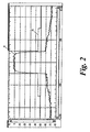
- Figure 2 shows a typical W-CDMA single channel spectrum.
- the plot 8 represents a transmitted signal (i.e. the output of the power amplifier) and the stepped line 10 represents the standard frequency mask.
- the spectrum shown in Figure 2 complies with the mask. However, at the point at which the adjacent channel power violates the boundary 4 of Figure 1 , it would expected that the spectrum of Figure 2 would violate the frequency mask.
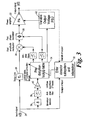
- Figure 3 shows a modified arrangement for introducing predistortion into an amplifier to compensate for non-linearities within the amplifier.
- a power amplifier 20 has a variable output voltage power supply unit 22.
- An input signal 24 is fed into the input of the power amplifier via an amplitude modulator 26 and a phase modulator 28.
- the delay line 30 is required simply to allow time for predistortion to be applied to the signal and may for the purposes of this explanation be ignored).
- a small portion (typically inductively coupled) of the output signal is fed back to an error detector subsystem 32 which compares a sample of the output with a sample of the input signal and carries out phase and amplitude error measurements.
- An envelope detector 36 and associated anti-aliasing filter 38 and quantizer 40 provides a quantized index for a predistortion look-up table 34. It will be noted for example from Figure 1 , distortion increases (generally speaking) with amplifier power output and therefore with envelope magnitude.
- the look-up table 34 contains mappings between measured input envelope and desired input (drive) values for the phase and amplitude modulators 28 and 26 required to correct for the phase and amplitude distortion generated by the amplifier.
- the contents of the look-up table are adjusted using feed-back of the actual measured phase and amplitude distortion at each envelope value 36 using the error detector subsystem and adaptation 32.
- the error detector subsystem 32 and the look-up table 34 co-operate to produce suitable predistortion values to be applied by the amplitude and phase modulators 26 and 28 to compensate for the measured distortion
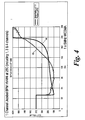
- the plot 42 shows look-up table values for phase correction (which corresponds to the amount of phase correction applied by the phase modulator 28) and look-up table values for the magnitude (or amplitude) correction applied by the amplitude modulator 26.
- the horizontal axis shows the values supplied by the envelope detector which is proportional to amplifier output power.
- variable output voltage power supply unit 22 supplies power to the amplifier and is controlled based on the operating position on the predistortion look-up table.
- a reduction in the power supply voltage typically will reduce the output power which may be produced by the amplifier without clipping.
- a reduction in the power supply voltage level may cause the amplifier to operate close to its clip point (i.e. may move the asymptotic portion of the line 44 in Figure 4 , towards the left of the graph).
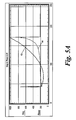
- Figure 5B shows an input envelope 'bin counter'. This 'bin counter' records the number of times during the last adaption cycle that each input envelope value was recorded. (in this implementation the counter stops at 16).
- the bin counter gives the system knowledge of the input signal envelope range during the last count (adaption) period.
- Figure 5B shows that during the last adaption period the highest input signal envelope was recorded at a value of approximately 170. This knowledge is combined with data from the correction look up tables ( Figure 5A ) to determine how close the system is to clip. If the amplitude and/or phase correction values in the look up table are below their maximum allowed values at the peak input level, then the system is operating above clip.
- a feedback algorithm may be used to reduce the power supply voltage until the maximum applied amplitude predistortion corresponds to a value of 1000 in the look-up table.
- This allows an additional 23 values as a margin (it will be noted that the values given in the plots of Figures 4 and 5 are binary values which is a consequence of the use typically of digital to analogue converters for controlling the variable voltage passed by unit 22 and the modulators 26 and 28).
- phase and/or amplitude curves 42 and 44 may signal the onset of clipping.
- the advantage of operating the amplifier close to its clip point may clearly be seen with reference to Figures 6 and 7 .
- the lines 50 in the two graphs represent adjacent channel power (adjacent channel power ratio in Figure 7 ) and therefore correspond to distortion in the amplifier power output.
- the lines 50 have a knee and an asymptotic portion which corresponds to amplifier clipping.
- the solid lines 52 also correspond to the defined boundaries in the transmission standards which must not be violated in order to meet the standards.
- the other lines 54 represent amplifier efficiency (in terms of DC power in versus RF power out). It will be noted that the amplifier efficiency increases dramatically as operation of the amplifier occurs closer to the clip point.
- the output characteristic of the amplifier which has been measured is phase and/or amplitude distortion.
- An alternative technique is described below which involves the use of a spectral analysis of the output signal. This technique allows a power amplifier to be used at or very close to its maximum power output thus reducing the margin which is required to allow for worst case operating conditions and/or unit-to-unit variations and also potentially offering the efficiency benefits discussed above. It will be appreciated also that both techniques could be used together.
- a simple receiver (which may for example mix the signal down to an intermediate frequency or base band) is applied to the output of the amplifier and a simple spectrum analyser (for example implemented in an FPGA or ASIC component) is used to process the "received" signal.
- a simple spectrum analyser for example implemented in an FPGA or ASIC component
- a base station includes a transmit application specific integrated circuit (ASIC) 60 which provides a two channel input into a BBPD field programmable gate array (FPGA).
- ASIC application specific integrated circuit
- FPGA field programmable gate array
- the output of the FPGA is fed into a pair of digital-to-analog converters 64-1 and 64-2 and then to a pair of anti-aliasing filters 66-1 and 66-2.
- the signal is then amplified and up-mixed together using a pair of amplifiers 68-1 and 68-2 and a mixer 70.
- the signal is then buffered and passed through a variable gain device 72. After band pass filtering, the signal is passed to a power amplifier 74. With the exception of the FPGA 62, this is the generally conventional arrangement.
- circuit of Figure 8 has been furthered modified with the addition of a feedback loop which takes an inductive 'sniff' from the output of the power amplifier 74 and includes a variable gain device 76, a downmixer 78.an amplifier 80 and a pair of bandpass filter 82 and 84.
- the feedback signal is then isolated (isolator 86) and sampled using an analog-to-digital converter 88.
- the digitised, down-mixed signal is then fed back into the FPGA 62.
- the signal may be compared with the frequency mask (for example the type of mask shown in Figure 2 ) and the amplifier output power adjusted accordingly using the variable gain devices 72 and/or 76 until it is determined that it does not violate to frequency mask 10.
- the gain of the amplifier or the gain of the transceiver may be varied in order to maximise output power for a given amplifier and power supply voltage (as is also possible for the first embodiment) or the power supply voltage may be varied in order to improve amplifier efficiency consistent with meeting the frequency mask 10 of Figure 2 as described above.
- a particular advantage of implementing an integral spectrum analyser is that other qualitative measurements may be made on the signal, for example wave form quality, error vector magnitude and/or code domain noise. This may be measured and monitored remotely. This may further reduce base station operating costs since it may be used to reduce the frequency of visits which are required to a particular base station sight.
- the measurements of the output may be used to provide an integral diagnostic capability. This may be achieved, for example, by including typical values in the base station processing hardware which are compared with the measured values. When the measured values differ from the stored values by more than a predetermined amount, an error may be flagged since this may represent a developing or developed fault within the base station.
- a significant part of the cost of a base station in the cellular mobile radio system is the power amplifier.
- the power amplifier it is desirable to maximise usage of a power amplifier and in particular to gain the best power output from the amplifier or to improve its efficiency.
- Such power amplifiers must operate within strict spectral boundaries and thus power amplifiers are typically over-specified in order to ensure that the spectral requirements are met.
- the degree of over-specification of the amplifier required may be reduced with consequent cost and environmental savings.
Landscapes
- Engineering & Computer Science (AREA)
- Power Engineering (AREA)
- Physics & Mathematics (AREA)
- Nonlinear Science (AREA)
- Amplifiers (AREA)
- Transmitters (AREA)
Claims (19)
- Verzerrungsregelkreis (26, 28, 32, 34) für einen Leistungsverstärker (20), umfassend:ein Ausgangsmessmittel, das zum Messen einer vorbestimmten Ausgangseigenschaft eines Ausgangssignals (y(t)) des Verstärkers (20) betriebsfähig ist;ein Verarbeitungsmittel (32) zum Verarbeiten der vom Ausgangsmessmittel erzeugten Messung;ein Mittel (26, 28), das zum Anlegen einer Vorverzerrung an ein Eingangssignal (x(t) des Verstärkers betriebsfähig ist;wobei der Regler (26, 28, 32, 34) gekennzeichnet ist durch:ein Reglermittel (34) zum Bestimmen eines Ausmaßes an Vorverzerrung, das für die Verzerrung repräsentativ ist, die vom Verstärker (20) in das Verstärkerausgangssignal eingeführt wird;das Mittel (26, 28), das zum Anlegen einer Vorverzerrung betriebsfähig ist, eine Vorverzerrung an das Eingangssignal (x(t) des Verstärkers auf der Basis des bestimmten Ausmaßes an Vorverzerrung anlegt;wobei das Reglermittel (34) zum Einstellen des Betriebsparameters des Verstärkers auch als Reaktion auf dasselbe bestimmte Ausmaß einer Vorverzerrung ausgebildet ist und wobei das Verarbeitungsmittel (32) zum Verarbeiten der gemessenen vorbestimmten Ausgangseigenschaft ausgebildet ist, um eine Eigenschaftskurve von Korrekturwerten gegenüber Verstärkerausgangsleistungswerten zu erstellen; unddas Reglermittel (34) zum periodischen Einstellen des Betriebsparameters des Verstärkers (20) ausgebildet ist, so dass ein Wert des Verstärkerleistungsausgangs unmittelbar unter einem Punkt auf der Eigenschaftskurve bleibt, an dem ein Gradient der Kurve asymptotisch wird.
- Regler (26, 28, 32, 34) nach Anspruch 1, wobei die gemessene vorbestimmte Ausgangseigenschaft eine Phasenverzerrung des Verstärkerausgangs ist.
- Regler (26, 28, 32, 34) nach einem der Ansprüche 1 bis 2, wobei die gemessene vorbestimmte Ausgangseigenschaft eine Amplitudenverzerrung des Verstärkerausgangs ist.
- Regler (26, 28, 32, 34) nach Anspruch 1, wobei die gemessene vorbestimmte Ausgangseigenschaft ein Frequenzspektrum des Verstärkerausgangs ist.
- Regler (26, 28, 32, 34) nach einem der Ansprüche 1 bis 4, wobei der Betriebsparameter die Ausgangsspannung einer Leistungsversorgung (22) ist, die zum Zuführen von Leistung zum Leistungsverstärker ausgebildet ist.
- Regler (26, 28, 32, 34) nach einem der Ansprüche 1 bis 5, wobei der Betriebsparameter die Verstärkung des Leistungsverstärkers (20) ist.
- Verfahren zum Optimieren des Wirkungsgrades in einem Leistungsverstärker (20), umfassend:Messen einer vorbestimmten Ausgangseigenschaft eines Ausgangssignals (y(t) des Verstärkers (20);Verarbeiten der gemessenen vorbestimmten Ausgangseigenschaft;Anlegen einer Vorverzerrung an ein Eingangssignal (x(t) des Verstärkers;zur Bestimmung eines Ausmaßes an Vorverzerrung, die für die Verzerrung repräsentativ ist, die vom Verstärker (20) in das Verstärkerausgangssignal eingeführt wird; Anlegen einer Vorverzerrung an das Eingangssignal (x(t) des Verstärkers auf der Basis des bestimmten Ausmaßes an Vorverzerrung; undEinstellen eines Betriebsparameters des Verstärkers;wobei das Verfahren gekennzeichnet ist durchBestimmen eines Ausmaßes einer Vorverzerrung, das für die Verzerrung repräsentativ ist, die vom Verstärker (20) in das Verstärkerausgangssignal eingeführt wird;Anlegen einer Vorverzerrung an das Eingangssignal (x(t) des Verstärkers auf der Basis des bestimmten Ausmaßes einer Vorverzerrung;wobei der Betriebsparameters des Verstärkers auch als Reaktion auf dasselbe bestimmte Ausmaß einer Vorverzerrung eingestellt wird;wobei die gemessene vorbestimmte Ausgangseigenschaft verarbeitet wird, um eine Eigenschaftskurve von Korrekturwerten gegenüber Verstärkerausgangsleistungswerten zu erstellen; undder Betriebsparameter des Verstärkers (20) periodisch eingestellt wird, so dass ein Wert des Verstärkerleistungsausgangs unmittelbar unter einem Punkt auf der Eigenschaftskurve bleibt, an dem ein Gradient der Kurve asymptotisch wird.
- Verfahren nach Anspruch 7, wobei die gemessene vorbestimmte Ausgangseigenschaft eine Phasenverzerrung ist und wobei der Betriebsparameter des Verstärkers (20) so eingestellt ist, dass der Gradient sich der Unendlichkeit nähert, was für die Clipping-Verzerrung im Verstärker repräsentativ ist.
- Verfahren nach Anspruch 7 oder Anspruch 8, wobei die gemessene vorbestimmte Ausgangseigenschaft eine Amplitudenverzerrung ist und wobei der Betriebsparameter des Verstärkers (20) so eingestellt ist, dass der Gradient sich der Unendlichkeit nähert, was für die Clipping-Verzerrung im Verstärker repräsentativ ist.
- Verfahren nach einem der Ansprüche 7 bis 9, wobei der Betriebsparameter eine Spannung einer Leistungsversorgung (22) für den Leistungsverstärker (20) ist.
- Verfahren nach einem der Ansprüche 7 bis 10, wobei der Betriebsparameter die Verstärkung des Verstärkers ist.
- Verfahren nach Anspruch 7, des Weiteren umfassend das Vergleichen der gemessenen vorbestimmten Ausgangseigenschaft gegen einen vorbestimmten Schwellenwert und das periodische Einstellen des Ausgangsparameters zum Aufrechterhalten der gemessenen vorbestimmten Ausgangseigenschaft an einer gewünschten Seite des Schwellenwertes.
- Verfahren nach Anspruch 12, wobei die gemessene vorbestimmte Ausgangseigenschaft ein Frequenzspektrum des Ausgangs des Verstärkers (20) ist und der Schwellenwert eine vorbestimmte Spektralmaske ist.
- Verfahren nach Anspruch 12, wobei die gemessene vorbestimmte Ausgangseigenschaft eine Wellenformqualität des Ausgangs des Verstärkers (20) ist.
- Verfahren nach Anspruch 12, wobei die gemessene vorbestimmte Ausgangseigenschaft eine Fehlervektorgröße des Ausgangs des Verstärkers (20) ist.
- Verfahren nach Anspruch 12, wobei die gemessene vorbestimmte Ausgangseigenschaft ein Code-Domain-Rauschen im Ausgang des Verstärkers (20) ist.
- Leistungsverstärker (20), umfassend einen Verzerrungsregelkreis (26, 28, 32, 34) nach einem der Ansprüche 1 bis 7.
- Basisstation für ein Funknetz, umfassend einen Leistungsverstärker nach Anspruch 17.
- Drahtloses Kommunikationsnetz, umfassend eine Basisstation nach Anspruch 18.
Applications Claiming Priority (3)
| Application Number | Priority Date | Filing Date | Title |
|---|---|---|---|
| US35879 | 2001-12-26 | ||
| US10/035,879 US6703897B2 (en) | 2001-12-26 | 2001-12-26 | Methods of optimising power amplifier efficiency and closed-loop power amplifier controllers |
| PCT/GB2002/005737 WO2003061114A2 (en) | 2001-12-26 | 2002-12-18 | Methods of optimising power amplifier efficiency and closed-loop power amplifier controllers |
Publications (2)
| Publication Number | Publication Date |
|---|---|
| EP1464112A2 EP1464112A2 (de) | 2004-10-06 |
| EP1464112B1 true EP1464112B1 (de) | 2012-10-24 |
Family
ID=21885326
Family Applications (1)
| Application Number | Title | Priority Date | Filing Date |
|---|---|---|---|
| EP02788140A Expired - Lifetime EP1464112B1 (de) | 2001-12-26 | 2002-12-18 | Verfahrenen zur optimierung des wirkungsgrads eines leistungsverstärkers, und leistungverstärkerregler mit einem geschlossenen regelkreis |
Country Status (7)
| Country | Link |
|---|---|
| US (1) | US6703897B2 (de) |
| EP (1) | EP1464112B1 (de) |
| KR (1) | KR100985044B1 (de) |
| CN (1) | CN100471042C (de) |
| AU (1) | AU2002352421A1 (de) |
| IL (1) | IL162683A0 (de) |
| WO (1) | WO2003061114A2 (de) |
Families Citing this family (65)
| Publication number | Priority date | Publication date | Assignee | Title |
|---|---|---|---|---|
| US6909757B2 (en) * | 2001-05-14 | 2005-06-21 | Ericsson Inc. | Methods, transmitters, and computer program products for transmitting a signal by adjusting a delay between an amplitude component of the signal and a phase component of the signal based on the transmission power |
| US7248642B1 (en) | 2002-02-05 | 2007-07-24 | Andrew Corporation | Frequency-dependent phase pre-distortion for reducing spurious emissions in communication networks |
| US7197085B1 (en) | 2002-03-08 | 2007-03-27 | Andrew Corporation | Frequency-dependent magnitude pre-distortion for reducing spurious emissions in communication networks |
| US7266159B2 (en) * | 2002-03-08 | 2007-09-04 | Andrew Corporation | Frequency-dependent magnitude pre-distortion on non-baseband input signals for reducing spurious emissions in communication networks |
| CN1177449C (zh) * | 2002-04-23 | 2004-11-24 | 华为技术有限公司 | 基于基带数字预失真技术的提高射频功率放大器效率的方法 |
| US8811917B2 (en) | 2002-05-01 | 2014-08-19 | Dali Systems Co. Ltd. | Digital hybrid mode power amplifier system |
| US8380143B2 (en) | 2002-05-01 | 2013-02-19 | Dali Systems Co. Ltd | Power amplifier time-delay invariant predistortion methods and apparatus |
| US8064850B2 (en) * | 2002-05-01 | 2011-11-22 | Dali Systems Co., Ltd. | High efficiency linearization power amplifier for wireless communication |
| US6985704B2 (en) * | 2002-05-01 | 2006-01-10 | Dali Yang | System and method for digital memorized predistortion for wireless communication |
| US8472897B1 (en) | 2006-12-22 | 2013-06-25 | Dali Systems Co. Ltd. | Power amplifier predistortion methods and apparatus |
| US7139327B2 (en) * | 2002-06-10 | 2006-11-21 | Andrew Corporation | Digital pre-distortion of input signals for reducing spurious emissions in communication networks |
| DE50213057D1 (de) * | 2002-07-17 | 2009-01-08 | Nokia Siemens Networks Gmbh | Verfahren und Vorrichtung zum Betreiben eines Sendeverstärkers |
| US7321635B2 (en) * | 2002-08-16 | 2008-01-22 | Andrew Corporation | Linearization of amplifiers using baseband detection and non-baseband pre-distortion |
| US7091777B2 (en) * | 2002-09-30 | 2006-08-15 | Lucent Technologies Inc. | Controller for an RF power amplifier |
| US7149484B2 (en) * | 2002-10-03 | 2006-12-12 | Intel Corporation | Portable communication device having adjustable amplification and method therefor |
| EP1548949A4 (de) * | 2002-10-03 | 2009-06-24 | Panasonic Corp | Sendeverfahren und sendervorrichtung |
| US7254195B2 (en) * | 2003-08-25 | 2007-08-07 | M/A-Com, Inc. | Apparatus, methods and articles of manufacture for dynamic differential delay correction |
| US7251293B2 (en) * | 2003-06-27 | 2007-07-31 | Andrew Corporation | Digital pre-distortion for the linearization of power amplifiers with asymmetrical characteristics |
| KR100518456B1 (ko) * | 2003-10-10 | 2005-09-30 | 학교법인 포항공과대학교 | 전력 증폭기의 선형화를 위한 디지털 피드백 선형화 장치및 방법 |
| JP2005167541A (ja) * | 2003-12-02 | 2005-06-23 | Matsushita Electric Ind Co Ltd | 送信機 |
| US7339426B2 (en) * | 2004-03-19 | 2008-03-04 | Powerwave Technologies, Inc. | High efficiency linear amplifier employing dynamically controlled back off |
| JP4417174B2 (ja) * | 2004-05-19 | 2010-02-17 | 株式会社日立国際電気 | プリディストータ |
| JP4801074B2 (ja) * | 2004-09-15 | 2011-10-26 | テレフオンアクチーボラゲット エル エム エリクソン(パブル) | 信号プリディストーションに関する装置と方法 |
| US7706467B2 (en) * | 2004-12-17 | 2010-04-27 | Andrew Llc | Transmitter with an envelope tracking power amplifier utilizing digital predistortion of the signal envelope |
| GB2421373B (en) * | 2004-12-17 | 2009-01-28 | Motorola Inc | A transmitter a transceiver and method of controlling a transmit power therefor |
| EP1708360A1 (de) * | 2005-03-30 | 2006-10-04 | Siemens Aktiengesellschaft | Verfahren und Vorrichtung zur Erzeugung eines Hochfrequenzsignals |
| US7653147B2 (en) * | 2005-08-17 | 2010-01-26 | Intel Corporation | Transmitter control |
| CN100442884C (zh) * | 2005-12-16 | 2008-12-10 | 上海华为技术有限公司 | 无线通信网络中节省基站功耗的方法及其系统 |
| KR100725982B1 (ko) * | 2006-02-03 | 2007-06-08 | 삼성전자주식회사 | 전압 변동에 따른 기록 파라미터 조절방법과 조절장치 |
| DE102006020831B4 (de) * | 2006-05-04 | 2014-08-28 | Siemens Aktiengesellschaft | Regler für einen Hochfrequenzverstärker |
| US7541866B2 (en) * | 2006-09-29 | 2009-06-02 | Nortel Networks Limited | Enhanced doherty amplifier with asymmetrical semiconductors |
| US20080122542A1 (en) * | 2006-11-27 | 2008-05-29 | Gregory Bowles | Enhanced amplifier with auxiliary path bias modulation |
| US9026067B2 (en) * | 2007-04-23 | 2015-05-05 | Dali Systems Co. Ltd. | Remotely reconfigurable power amplifier system and method |
| KR20100014339A (ko) * | 2006-12-26 | 2010-02-10 | 달리 시스템즈 씨오. 엘티디. | 다중 채널 광대역 통신 시스템에서의 기저 대역 전치 왜곡 선형화를 위한 방법 및 시스템 |
| JP2008206062A (ja) * | 2007-02-22 | 2008-09-04 | Fujitsu Ltd | 電源装置、信号出力装置、および電源供給方法 |
| US8274332B2 (en) | 2007-04-23 | 2012-09-25 | Dali Systems Co. Ltd. | N-way Doherty distributed power amplifier with power tracking |
| US7688135B2 (en) * | 2007-04-23 | 2010-03-30 | Dali Systems Co. Ltd. | N-way Doherty distributed power amplifier |
| FI20075343A0 (fi) * | 2007-05-11 | 2007-05-11 | Nokia Corp | Lähettimen häiriönpäästön ohjaus |
| US8224266B2 (en) * | 2007-08-30 | 2012-07-17 | Dali Systems Co., Ltd. | Power amplifier predistortion methods and apparatus using envelope and phase detector |
| KR101669173B1 (ko) | 2007-12-07 | 2016-10-25 | 달리 시스템즈 씨오. 엘티디. | 베이스밴드-도출형 광대역 rf 디지털 전치 왜곡 시스템 |
| US7768353B2 (en) | 2008-06-13 | 2010-08-03 | Samsung Electro-Mechanics Company, Ltd. | Systems and methods for switching mode power amplifier control |
| US7944294B2 (en) * | 2008-06-27 | 2011-05-17 | Cambridge Silicon Radio Limited | Signal amplification |
| GB2466218B (en) * | 2008-12-12 | 2012-02-01 | Motorola Solutions Inc | Simultaneous supply modulation and circulator elimination with maximum efficiency |
| JP5365369B2 (ja) * | 2009-06-26 | 2013-12-11 | 富士通株式会社 | 送信装置、歪み補償装置及び歪み補償方法 |
| GB2480687B (en) * | 2010-05-28 | 2018-04-04 | Snaptrack Inc | Power supply pre-distortion |
| US8183917B2 (en) | 2010-06-04 | 2012-05-22 | Quantance, Inc. | RF power amplifier circuit with mismatch tolerance |
| US8565343B1 (en) * | 2010-06-29 | 2013-10-22 | Qualcomm Incorporated | Transmit power control utilizing loopback error vector magnitude thresholds |
| US8599962B1 (en) * | 2010-07-16 | 2013-12-03 | Marvell International Ltd. | Power control using distortion measurement |
| KR102136940B1 (ko) | 2010-09-14 | 2020-07-23 | 달리 시스템즈 씨오. 엘티디. | 원격으로 재구성가능한 분산 안테나 시스템 및 방법 |
| US8610499B2 (en) * | 2011-04-11 | 2013-12-17 | Auriga Measurement Systems, LLC | Radio frequency (RF) amplifier utilizing a predistortion circuit and related techniques |
| US8711976B2 (en) | 2011-05-12 | 2014-04-29 | Andrew Llc | Pre-distortion architecture for compensating non-linear effects |
| US8879665B2 (en) * | 2011-06-08 | 2014-11-04 | Broadcom Corporation | Controlling a power amplifier based on transmitter output emissions |
| US9041464B2 (en) * | 2011-09-16 | 2015-05-26 | Qualcomm Incorporated | Circuitry for reducing power consumption |
| JPWO2013145748A1 (ja) * | 2012-03-30 | 2015-12-10 | 日本電気株式会社 | 増幅器および増幅方法 |
| GB2503890A (en) * | 2012-07-10 | 2014-01-15 | Nujira Ltd | Switched mode power supply having interference suppression capacitors |
| CN103905357B (zh) * | 2012-12-28 | 2017-05-10 | 京信通信系统(中国)有限公司 | 一种信号预失真处理方法及装置 |
| KR102048235B1 (ko) * | 2013-04-10 | 2019-11-25 | 삼성전자주식회사 | 무선 통신 시스템에서 디지털 전치 왜곡 장치 및 방법 |
| US10038503B2 (en) * | 2014-08-13 | 2018-07-31 | Xilinx, Inc. | Adaptive optical channel compensation |
| US9479122B2 (en) * | 2014-08-28 | 2016-10-25 | Macom Technology Solutions Holdings, Inc. | Amplification phase correction in a pulse burst |
| US9374262B1 (en) * | 2014-12-18 | 2016-06-21 | Viasat, Inc. | Techniques for linearizing phase separately from amplitude in a communications system |
| US9787259B2 (en) * | 2015-11-06 | 2017-10-10 | Infineon Technologies Ag | Outphasing power amplifier signal splitter using next stage input impedance and multiple biasing |
| US9853599B2 (en) * | 2015-12-04 | 2017-12-26 | The Boeing Company | Simultaneous linearization of multiple power amplifiers with independent power |
| US9985590B2 (en) | 2016-01-27 | 2018-05-29 | Mediatek Inc. | Adaptive power amplifier supply with pre-distortion mechanism |
| US9755585B1 (en) * | 2016-09-06 | 2017-09-05 | Aero Antenna, Inc. | High power radio frequency amplifier with dynamic digital control |
| JP6883659B2 (ja) * | 2017-04-28 | 2021-06-09 | パナソニック インテレクチュアル プロパティ コーポレーション オブ アメリカPanasonic Intellectual Property Corporation of America | 測定装置及び測定方法 |
Family Cites Families (20)
| Publication number | Priority date | Publication date | Assignee | Title |
|---|---|---|---|---|
| JPH03198512A (ja) * | 1989-12-27 | 1991-08-29 | Mitsubishi Electric Corp | 高周波増幅器 |
| JPH0440105A (ja) * | 1990-06-06 | 1992-02-10 | Oki Electric Ind Co Ltd | 線形化増幅回路 |
| JPH07118617B2 (ja) * | 1990-07-19 | 1995-12-18 | 沖電気工業株式会社 | 電力増幅装置及び送信装置 |
| US5742201A (en) * | 1996-01-30 | 1998-04-21 | Spectrian | Polar envelope correction mechanism for enhancing linearity of RF/microwave power amplifier |
| US5892397A (en) * | 1996-03-29 | 1999-04-06 | Spectrian | Adaptive compensation of RF amplifier distortion by injecting predistortion signal derived from respectively different functions of input signal amplitude |
| WO1997049174A1 (de) * | 1996-06-19 | 1997-12-24 | Fraunhofer-Gesellschaft zur Förderung der angewandten Forschung e.V. | Vorverzerrung für eine nichtlineare übertragungsstrecke im hochfrequenzbereich |
| US5923712A (en) * | 1997-05-05 | 1999-07-13 | Glenayre Electronics, Inc. | Method and apparatus for linear transmission by direct inverse modeling |
| US6072364A (en) * | 1997-06-17 | 2000-06-06 | Amplix | Adaptive digital predistortion for power amplifiers with real time modeling of memoryless complex gains |
| US6081161A (en) * | 1998-05-18 | 2000-06-27 | Omnipoint Corporation | Amplifier with dynamatically adaptable supply voltage |
| US6519293B1 (en) * | 1998-06-03 | 2003-02-11 | Mitsubishi Denki Kabushiki Kaisha | Radio transmitter and radio communication method |
| KR100326176B1 (ko) * | 1998-08-06 | 2002-04-17 | 윤종용 | 이동통신시스템의전력증폭장치및방법 |
| US6069530A (en) * | 1998-09-16 | 2000-05-30 | Motorola, Inc. | Apparatus and method for linear power amplification |
| US6275685B1 (en) * | 1998-12-10 | 2001-08-14 | Nortel Networks Limited | Linear amplifier arrangement |
| ES2247737T3 (es) * | 1998-12-24 | 2006-03-01 | Nokia Corporation | Transmisor multifrecuencia que usa la predistorsion y metodo de transmision. |
| US6043707A (en) * | 1999-01-07 | 2000-03-28 | Motorola, Inc. | Method and apparatus for operating a radio-frequency power amplifier as a variable-class linear amplifier |
| US6693974B2 (en) * | 1999-08-05 | 2004-02-17 | Samsung Electronics Co., Ltd. | Adaptive digital pre-distortion circuit using adjacent channel power profile and method of operation |
| CA2329100A1 (en) * | 1999-12-21 | 2001-06-21 | Nortel Networks Limited | Phase and amplitude detector and method of determining errors |
| US6366177B1 (en) * | 2000-02-02 | 2002-04-02 | Tropian Inc. | High-efficiency power modulators |
| US6396350B2 (en) * | 2000-02-09 | 2002-05-28 | Paradigm Wireless Systems, Inc. | Power booster method and apparatus for improving the performance of radio frequency linear power amplifiers |
| JP4622386B2 (ja) * | 2004-08-24 | 2011-02-02 | タカタ株式会社 | エアバッグ及びエアバッグ装置 |
-
2001
- 2001-12-26 US US10/035,879 patent/US6703897B2/en not_active Expired - Lifetime
-
2002
- 2002-12-18 AU AU2002352421A patent/AU2002352421A1/en not_active Abandoned
- 2002-12-18 IL IL16268302A patent/IL162683A0/xx unknown
- 2002-12-18 KR KR1020047010153A patent/KR100985044B1/ko not_active Expired - Fee Related
- 2002-12-18 WO PCT/GB2002/005737 patent/WO2003061114A2/en not_active Ceased
- 2002-12-18 CN CNB028261119A patent/CN100471042C/zh not_active Expired - Fee Related
- 2002-12-18 EP EP02788140A patent/EP1464112B1/de not_active Expired - Lifetime
Also Published As
| Publication number | Publication date |
|---|---|
| KR100985044B1 (ko) | 2010-10-04 |
| IL162683A0 (en) | 2005-11-20 |
| AU2002352421A8 (en) | 2003-07-30 |
| CN1636314A (zh) | 2005-07-06 |
| KR20040069346A (ko) | 2004-08-05 |
| US6703897B2 (en) | 2004-03-09 |
| EP1464112A2 (de) | 2004-10-06 |
| WO2003061114A3 (en) | 2004-05-27 |
| AU2002352421A1 (en) | 2003-07-30 |
| CN100471042C (zh) | 2009-03-18 |
| WO2003061114A2 (en) | 2003-07-24 |
| US20030117215A1 (en) | 2003-06-26 |
Similar Documents
| Publication | Publication Date | Title |
|---|---|---|
| US6703897B2 (en) | Methods of optimising power amplifier efficiency and closed-loop power amplifier controllers | |
| US5452473A (en) | Reverse link, transmit power correction and limitation in a radiotelephone system | |
| US5748678A (en) | Radio communications apparatus | |
| US6864745B2 (en) | Distortion compensation device | |
| CA2233692C (en) | Linearized digital automatic gain control | |
| EP2795792B1 (de) | Adaptive vorverzerrung für ein nichtlineares subsystem auf basis eines modells als verkettungen eines nichtlinearen, gefolgt von einem linearen modell | |
| US7970364B2 (en) | Strategy for using the envelope information within a closed loop power control system | |
| CA2262361C (en) | Method and apparatus for tailored distortion of a signal prior to amplification | |
| US5675287A (en) | Digital DC correction circuit for a linear transmitter | |
| US20130107926A1 (en) | Controlling a Power Amplifier Based on Transmitter Output Emissions | |
| US8270916B2 (en) | Methods for tuning and controlling output power in polar transmitters | |
| GB2323987A (en) | A radio transceiver amplifier with closed loop gain control feedback for a trunked mode and open loop bias feedback for a direct mode | |
| US20110261903A1 (en) | Wireless communication unit, integrated circuit and method of power control of a power amplifier therefor | |
| EP1124324A1 (de) | Verfahren zur Linearisierung eines Sendesystems über ein breites Frequenzband mit einem Leistungsverstärker | |
| GB2283629A (en) | Splatter-reduced training for adaptive pre-distortion or cartesian feedback linearizers | |
| GB2337169A (en) | An adaptive predistorter for an amplifier | |
| KR20250020404A (ko) | 신호 증폭 회로부 | |
| Zhang et al. | An improved digital predistortion in wideband wireless transmitters using an under-sampled feedback loop | |
| EP1601096A1 (de) | Verfahren und elektronische Schleifenschaltung zur Einstellung der Vorspannung | |
| GB2329538A (en) | Reducing splatter from TDMA transmitter | |
| EP2377282B1 (de) | Sender mit verringerter spektraler verbreiterung und zugehörige verfahren | |
| GB2309342A (en) | Linear TDMA transmitter using selectable gain elements in forward and feedback paths | |
| KR20050034520A (ko) | 무선 송신기 | |
| Long et al. | A Lightweight Coefficient Update Method for Linearization of Power Amplifiers With Frequent Power Variation | |
| CA2275156C (en) | Reverse link, transmit power correction and limitation in a radiotelephone system |
Legal Events
| Date | Code | Title | Description |
|---|---|---|---|
| PUAI | Public reference made under article 153(3) epc to a published international application that has entered the european phase |
Free format text: ORIGINAL CODE: 0009012 |
|
| AK | Designated contracting states |
Kind code of ref document: A2 Designated state(s): AT BE BG CH CY CZ DE DK EE ES FI FR GB GR IE IT LI LU MC NL PT SE SI SK TR |
|
| AX | Request for extension of the european patent |
Extension state: AL LT LV MK RO |
|
| 17P | Request for examination filed |
Effective date: 20041129 |
|
| 17Q | First examination report despatched |
Effective date: 20050303 |
|
| REG | Reference to a national code |
Ref country code: DE Ref legal event code: R079 Ref document number: 60243928 Country of ref document: DE Free format text: PREVIOUS MAIN CLASS: H03F0001000000 Ipc: H03F0001320000 |
|
| GRAP | Despatch of communication of intention to grant a patent |
Free format text: ORIGINAL CODE: EPIDOSNIGR1 |
|
| RIC1 | Information provided on ipc code assigned before grant |
Ipc: H03F 1/02 20060101ALI20120330BHEP Ipc: H03F 1/32 20060101AFI20120330BHEP |
|
| GRAS | Grant fee paid |
Free format text: ORIGINAL CODE: EPIDOSNIGR3 |
|
| GRAA | (expected) grant |
Free format text: ORIGINAL CODE: 0009210 |
|
| AK | Designated contracting states |
Kind code of ref document: B1 Designated state(s): AT BE BG CH CY CZ DE DK EE ES FI FR GB GR IE IT LI LU MC NL PT SE SI SK TR |
|
| REG | Reference to a national code |
Ref country code: GB Ref legal event code: FG4D |
|
| REG | Reference to a national code |
Ref country code: CH Ref legal event code: EP |
|
| REG | Reference to a national code |
Ref country code: AT Ref legal event code: REF Ref document number: 581363 Country of ref document: AT Kind code of ref document: T Effective date: 20121115 |
|
| REG | Reference to a national code |
Ref country code: IE Ref legal event code: FG4D |
|
| REG | Reference to a national code |
Ref country code: DE Ref legal event code: R096 Ref document number: 60243928 Country of ref document: DE Effective date: 20121220 |
|
| REG | Reference to a national code |
Ref country code: SE Ref legal event code: TRGR |
|
| RAP2 | Party data changed (patent owner data changed or rights of a patent transferred) |
Owner name: APPLE INC. |
|
| REG | Reference to a national code |
Ref country code: AT Ref legal event code: MK05 Ref document number: 581363 Country of ref document: AT Kind code of ref document: T Effective date: 20121024 |
|
| REG | Reference to a national code |
Ref country code: NL Ref legal event code: VDEP Effective date: 20121024 |
|
| PG25 | Lapsed in a contracting state [announced via postgrant information from national office to epo] |
Ref country code: ES Free format text: LAPSE BECAUSE OF FAILURE TO SUBMIT A TRANSLATION OF THE DESCRIPTION OR TO PAY THE FEE WITHIN THE PRESCRIBED TIME-LIMIT Effective date: 20130204 Ref country code: NL Free format text: LAPSE BECAUSE OF FAILURE TO SUBMIT A TRANSLATION OF THE DESCRIPTION OR TO PAY THE FEE WITHIN THE PRESCRIBED TIME-LIMIT Effective date: 20121024 |
|
| REG | Reference to a national code |
Ref country code: DE Ref legal event code: R081 Ref document number: 60243928 Country of ref document: DE Owner name: APPLE INC., US Free format text: FORMER OWNER: NORTEL NETWORKS LIMITED, ST. LAURENT, CA Effective date: 20130404 Ref country code: DE Ref legal event code: R081 Ref document number: 60243928 Country of ref document: DE Owner name: APPLE INC., US Free format text: FORMER OWNER: NORTEL NETWORKS LTD., ST. LAURENT, CA Effective date: 20121024 Ref country code: DE Ref legal event code: R082 Ref document number: 60243928 Country of ref document: DE Representative=s name: BARDEHLE PAGENBERG PARTNERSCHAFT PATENTANWAELT, DE Effective date: 20130404 Ref country code: DE Ref legal event code: R082 Ref document number: 60243928 Country of ref document: DE Representative=s name: BARDEHLE PAGENBERG PARTNERSCHAFT MBB PATENTANW, DE Effective date: 20130404 Ref country code: DE Ref legal event code: R081 Ref document number: 60243928 Country of ref document: DE Owner name: APPLE INC., CUPERTINO, US Free format text: FORMER OWNER: NORTEL NETWORKS LTD., ST. LAURENT, QUEBEC, CA Effective date: 20121024 Ref country code: DE Ref legal event code: R081 Ref document number: 60243928 Country of ref document: DE Owner name: APPLE INC., CUPERTINO, US Free format text: FORMER OWNER: NORTEL NETWORKS LIMITED, ST. LAURENT, QUEBEC, CA Effective date: 20130404 |
|
| REG | Reference to a national code |
Ref country code: GB Ref legal event code: 732E Free format text: REGISTERED BETWEEN 20130502 AND 20130508 |
|
| PG25 | Lapsed in a contracting state [announced via postgrant information from national office to epo] |
Ref country code: GR Free format text: LAPSE BECAUSE OF FAILURE TO SUBMIT A TRANSLATION OF THE DESCRIPTION OR TO PAY THE FEE WITHIN THE PRESCRIBED TIME-LIMIT Effective date: 20130125 Ref country code: CY Free format text: LAPSE BECAUSE OF FAILURE TO SUBMIT A TRANSLATION OF THE DESCRIPTION OR TO PAY THE FEE WITHIN THE PRESCRIBED TIME-LIMIT Effective date: 20121024 Ref country code: SI Free format text: LAPSE BECAUSE OF FAILURE TO SUBMIT A TRANSLATION OF THE DESCRIPTION OR TO PAY THE FEE WITHIN THE PRESCRIBED TIME-LIMIT Effective date: 20121024 Ref country code: PT Free format text: LAPSE BECAUSE OF FAILURE TO SUBMIT A TRANSLATION OF THE DESCRIPTION OR TO PAY THE FEE WITHIN THE PRESCRIBED TIME-LIMIT Effective date: 20130225 Ref country code: BE Free format text: LAPSE BECAUSE OF FAILURE TO SUBMIT A TRANSLATION OF THE DESCRIPTION OR TO PAY THE FEE WITHIN THE PRESCRIBED TIME-LIMIT Effective date: 20121024 |
|
| REG | Reference to a national code |
Ref country code: GB Ref legal event code: 732E Free format text: REGISTERED BETWEEN 20130509 AND 20130515 |
|
| PG25 | Lapsed in a contracting state [announced via postgrant information from national office to epo] |
Ref country code: AT Free format text: LAPSE BECAUSE OF FAILURE TO SUBMIT A TRANSLATION OF THE DESCRIPTION OR TO PAY THE FEE WITHIN THE PRESCRIBED TIME-LIMIT Effective date: 20121024 |
|
| PG25 | Lapsed in a contracting state [announced via postgrant information from national office to epo] |
Ref country code: BG Free format text: LAPSE BECAUSE OF FAILURE TO SUBMIT A TRANSLATION OF THE DESCRIPTION OR TO PAY THE FEE WITHIN THE PRESCRIBED TIME-LIMIT Effective date: 20130124 Ref country code: SK Free format text: LAPSE BECAUSE OF FAILURE TO SUBMIT A TRANSLATION OF THE DESCRIPTION OR TO PAY THE FEE WITHIN THE PRESCRIBED TIME-LIMIT Effective date: 20121024 Ref country code: EE Free format text: LAPSE BECAUSE OF FAILURE TO SUBMIT A TRANSLATION OF THE DESCRIPTION OR TO PAY THE FEE WITHIN THE PRESCRIBED TIME-LIMIT Effective date: 20121024 Ref country code: CZ Free format text: LAPSE BECAUSE OF FAILURE TO SUBMIT A TRANSLATION OF THE DESCRIPTION OR TO PAY THE FEE WITHIN THE PRESCRIBED TIME-LIMIT Effective date: 20121024 Ref country code: MC Free format text: LAPSE BECAUSE OF NON-PAYMENT OF DUE FEES Effective date: 20121231 Ref country code: DK Free format text: LAPSE BECAUSE OF FAILURE TO SUBMIT A TRANSLATION OF THE DESCRIPTION OR TO PAY THE FEE WITHIN THE PRESCRIBED TIME-LIMIT Effective date: 20121024 |
|
| REG | Reference to a national code |
Ref country code: CH Ref legal event code: PL |
|
| PG25 | Lapsed in a contracting state [announced via postgrant information from national office to epo] |
Ref country code: IT Free format text: LAPSE BECAUSE OF FAILURE TO SUBMIT A TRANSLATION OF THE DESCRIPTION OR TO PAY THE FEE WITHIN THE PRESCRIBED TIME-LIMIT Effective date: 20121024 |
|
| PLBE | No opposition filed within time limit |
Free format text: ORIGINAL CODE: 0009261 |
|
| STAA | Information on the status of an ep patent application or granted ep patent |
Free format text: STATUS: NO OPPOSITION FILED WITHIN TIME LIMIT |
|
| REG | Reference to a national code |
Ref country code: IE Ref legal event code: MM4A |
|
| 26N | No opposition filed |
Effective date: 20130725 |
|
| PG25 | Lapsed in a contracting state [announced via postgrant information from national office to epo] |
Ref country code: IE Free format text: LAPSE BECAUSE OF NON-PAYMENT OF DUE FEES Effective date: 20121218 Ref country code: CH Free format text: LAPSE BECAUSE OF NON-PAYMENT OF DUE FEES Effective date: 20121231 Ref country code: LI Free format text: LAPSE BECAUSE OF NON-PAYMENT OF DUE FEES Effective date: 20121231 |
|
| REG | Reference to a national code |
Ref country code: DE Ref legal event code: R097 Ref document number: 60243928 Country of ref document: DE Effective date: 20130725 |
|
| PG25 | Lapsed in a contracting state [announced via postgrant information from national office to epo] |
Ref country code: TR Free format text: LAPSE BECAUSE OF FAILURE TO SUBMIT A TRANSLATION OF THE DESCRIPTION OR TO PAY THE FEE WITHIN THE PRESCRIBED TIME-LIMIT Effective date: 20121024 |
|
| PG25 | Lapsed in a contracting state [announced via postgrant information from national office to epo] |
Ref country code: LU Free format text: LAPSE BECAUSE OF NON-PAYMENT OF DUE FEES Effective date: 20121218 |
|
| PGFP | Annual fee paid to national office [announced via postgrant information from national office to epo] |
Ref country code: GB Payment date: 20141217 Year of fee payment: 13 Ref country code: SE Payment date: 20141211 Year of fee payment: 13 |
|
| PGFP | Annual fee paid to national office [announced via postgrant information from national office to epo] |
Ref country code: FR Payment date: 20141208 Year of fee payment: 13 |
|
| REG | Reference to a national code |
Ref country code: SE Ref legal event code: EUG |
|
| GBPC | Gb: european patent ceased through non-payment of renewal fee |
Effective date: 20151218 |
|
| PG25 | Lapsed in a contracting state [announced via postgrant information from national office to epo] |
Ref country code: SE Free format text: LAPSE BECAUSE OF NON-PAYMENT OF DUE FEES Effective date: 20151219 |
|
| REG | Reference to a national code |
Ref country code: FR Ref legal event code: ST Effective date: 20160831 |
|
| PG25 | Lapsed in a contracting state [announced via postgrant information from national office to epo] |
Ref country code: GB Free format text: LAPSE BECAUSE OF NON-PAYMENT OF DUE FEES Effective date: 20151218 |
|
| PG25 | Lapsed in a contracting state [announced via postgrant information from national office to epo] |
Ref country code: FR Free format text: LAPSE BECAUSE OF NON-PAYMENT OF DUE FEES Effective date: 20151231 |
|
| PGFP | Annual fee paid to national office [announced via postgrant information from national office to epo] |
Ref country code: FI Payment date: 20201209 Year of fee payment: 19 Ref country code: DE Payment date: 20201208 Year of fee payment: 19 |
|
| REG | Reference to a national code |
Ref country code: DE Ref legal event code: R119 Ref document number: 60243928 Country of ref document: DE |
|
| REG | Reference to a national code |
Ref country code: FI Ref legal event code: MAE |
|
| PG25 | Lapsed in a contracting state [announced via postgrant information from national office to epo] |
Ref country code: FI Free format text: LAPSE BECAUSE OF NON-PAYMENT OF DUE FEES Effective date: 20211218 |
|
| PG25 | Lapsed in a contracting state [announced via postgrant information from national office to epo] |
Ref country code: DE Free format text: LAPSE BECAUSE OF NON-PAYMENT OF DUE FEES Effective date: 20220701 |