EP1454412B1 - Filter device and method of fabricating a filter device - Google Patents
Filter device and method of fabricating a filter device Download PDFInfo
- Publication number
- EP1454412B1 EP1454412B1 EP01274644A EP01274644A EP1454412B1 EP 1454412 B1 EP1454412 B1 EP 1454412B1 EP 01274644 A EP01274644 A EP 01274644A EP 01274644 A EP01274644 A EP 01274644A EP 1454412 B1 EP1454412 B1 EP 1454412B1
- Authority
- EP
- European Patent Office
- Prior art keywords
- filter
- substrate
- acoustic wave
- set forth
- filter device
- Prior art date
- Legal status (The legal status is an assumption and is not a legal conclusion. Google has not performed a legal analysis and makes no representation as to the accuracy of the status listed.)
- Expired - Lifetime
Links
Images


Classifications
-
- H—ELECTRICITY
- H03—ELECTRONIC CIRCUITRY
- H03H—IMPEDANCE NETWORKS, e.g. RESONANT CIRCUITS; RESONATORS
- H03H9/00—Networks comprising electromechanical or electro-acoustic elements; Electromechanical resonators
- H03H9/15—Constructional features of resonators consisting of piezoelectric or electrostrictive material
- H03H9/17—Constructional features of resonators consisting of piezoelectric or electrostrictive material having a single resonator
- H03H9/171—Constructional features of resonators consisting of piezoelectric or electrostrictive material having a single resonator implemented with thin-film techniques, i.e. of the film bulk acoustic resonator [FBAR] type
- H03H9/172—Means for mounting on a substrate, i.e. means constituting the material interface confining the waves to a volume
- H03H9/175—Acoustic mirrors
-
- H—ELECTRICITY
- H03—ELECTRONIC CIRCUITRY
- H03H—IMPEDANCE NETWORKS, e.g. RESONANT CIRCUITS; RESONATORS
- H03H3/00—Apparatus or processes specially adapted for the manufacture of impedance networks, resonating circuits, resonators
- H03H3/007—Apparatus or processes specially adapted for the manufacture of impedance networks, resonating circuits, resonators for the manufacture of electromechanical resonators or networks
- H03H3/02—Apparatus or processes specially adapted for the manufacture of impedance networks, resonating circuits, resonators for the manufacture of electromechanical resonators or networks for the manufacture of piezoelectric or electrostrictive resonators or networks
-
- H—ELECTRICITY
- H03—ELECTRONIC CIRCUITRY
- H03H—IMPEDANCE NETWORKS, e.g. RESONANT CIRCUITS; RESONATORS
- H03H9/00—Networks comprising electromechanical or electro-acoustic elements; Electromechanical resonators
- H03H9/02—Details
- H03H9/02007—Details of bulk acoustic wave devices
- H03H9/02047—Treatment of substrates
- H03H9/02055—Treatment of substrates of the surface including the back surface
-
- H—ELECTRICITY
- H03—ELECTRONIC CIRCUITRY
- H03H—IMPEDANCE NETWORKS, e.g. RESONANT CIRCUITS; RESONATORS
- H03H9/00—Networks comprising electromechanical or electro-acoustic elements; Electromechanical resonators
- H03H9/02—Details
- H03H9/02007—Details of bulk acoustic wave devices
- H03H9/02086—Means for compensation or elimination of undesirable effects
- H03H9/0211—Means for compensation or elimination of undesirable effects of reflections
-
- H—ELECTRICITY
- H03—ELECTRONIC CIRCUITRY
- H03H—IMPEDANCE NETWORKS, e.g. RESONANT CIRCUITS; RESONATORS
- H03H9/00—Networks comprising electromechanical or electro-acoustic elements; Electromechanical resonators
- H03H9/46—Filters
- H03H9/54—Filters comprising resonators of piezoelectric or electrostrictive material
- H03H9/58—Multiple crystal filters
- H03H9/582—Multiple crystal filters implemented with thin-film techniques
- H03H9/583—Multiple crystal filters implemented with thin-film techniques comprising a plurality of piezoelectric layers acoustically coupled
- H03H9/585—Stacked Crystal Filters [SCF]
-
- H—ELECTRICITY
- H03—ELECTRONIC CIRCUITRY
- H03H—IMPEDANCE NETWORKS, e.g. RESONANT CIRCUITS; RESONATORS
- H03H9/00—Networks comprising electromechanical or electro-acoustic elements; Electromechanical resonators
- H03H9/46—Filters
- H03H9/54—Filters comprising resonators of piezoelectric or electrostrictive material
- H03H9/58—Multiple crystal filters
- H03H9/582—Multiple crystal filters implemented with thin-film techniques
- H03H9/586—Means for mounting to a substrate, i.e. means constituting the material interface confining the waves to a volume
- H03H9/589—Acoustic mirrors
-
- Y—GENERAL TAGGING OF NEW TECHNOLOGICAL DEVELOPMENTS; GENERAL TAGGING OF CROSS-SECTIONAL TECHNOLOGIES SPANNING OVER SEVERAL SECTIONS OF THE IPC; TECHNICAL SUBJECTS COVERED BY FORMER USPC CROSS-REFERENCE ART COLLECTIONS [XRACs] AND DIGESTS
- Y10—TECHNICAL SUBJECTS COVERED BY FORMER USPC
- Y10T—TECHNICAL SUBJECTS COVERED BY FORMER US CLASSIFICATION
- Y10T29/00—Metal working
- Y10T29/42—Piezoelectric device making
Definitions
- the present invention relates to filter devices.
- the present invention especially relates to acoustic wave filter devices, e.g. Surface Acoustic Wave (SAW) filter devices, and/or Bulk Acoustic Wave (BAW) filter devices.
- SAW Surface Acoustic Wave
- BAW Bulk Acoustic Wave
- SAW Surface Acoustic Wave
- BAW Bulk Acoustic Wave filters
- Bulk Acoustic Wave (BAW) filters typically include several Bulk Acoustic Wave (BAW) resonators.
- BAW Bulk Acoustic Wave
- acoustic waves propagate in a direction that is perpendicular to the filter's layer surfaces.
- acoustic waves which propagate within a Surface Acoustic Wave (SAW) filter do so in a direction that is parallel to the layer surfaces of the filter.
- BAW Bulk Acoustic Wave
- FBARs Thin Film Bulk Acoustic Wave Resonators
- Bulk Acoustic Wave (BAW) filters can be fabricated to include various known types of Bulk Acoustic Wave (BAW) resonators. These known types of Bulk Acoustic Wave (BAW) resonators comprise three basic portions.
- a second one of the portions includes electrodes that are formed on opposite sides of the piezoelectric layer.
- a third portion of the Bulk Acoustic Wave (BAW) resonator includes a mechanism for acoustically isolating the substrate from vibrations produced by the piezoelectric layer.
- Bulk Acoustic Wave (BAW) resonators are typically fabricated on silicon, gallium arsenide, or glass substrates using thin film technology (e.g., sputtering, chemical vapor deposition, etc.).
- Bulk Acoustic Wave (BAW) resonators exhibit series and parallel resonances that are similar to those of, by example, crystal resonators.
- Resonant frequencies of Bulk Acoustic Wave (BAW) resonators can typically range from about 0.5 GH to 5 GHz, depending on the layer thicknesses of the devices.
- FIG. 1 shows an example of a Bulk-Acoustic-Wave (BAW) resonator using an acoustic mirror to acoustically isolate the resonator from the substrate.
- the Bulk Acoustic Wave (BAW) resonator 20 comprises a substrate 10 having a top surface 12 and a bottom surface 14. Acoustic mirror 31 overlies the top surface 12 of the substrate.
- the resonator further comprises a piezoelectric layer 22 interposed between a first electrode 21 and a second electrode 23, and a protective layer 16.
- the piezoelectric layer 22 comprises, by example, a piezoelectric material that can be fabricated as a thin film such as, by example, zinc-oxide (ZnO), or aluminum-nitride (AlN) .
- the acoustic mirror 31 comprises three layers, namely a top layer 31a, a middle layer 31b, and a bottom layer 31c.
- Each layer 31a, 31b and 31c has a thickness that is, by example, approximately equal to one quarter wavelength of the resonance frequency of the resonator.
- the top layer 31a and bottom layer 31c are made of materials having low acoustic impedances such as, by example, silicon oxide (SiO 2 ), poly-silicon, aluminum (Al) , or a polymer.
- the middle layer 31b is made of a material having a high acoustic impedance such as, by example, gold (Au), molybdenum (Mo), or tungsten (W).
- the substrate 10 may be comprised of various high acoustic impedance materials or low acoustic impedance materials (e.g., Si, SiO 2 , GaAs, glass, or a ceramic material).
- the number of layers in an acoustic mirror can vary broadly depending on the degree of acoustic isolation required for the respective filter device. Usually three to up to nine layers are used, wherein uneven and even numbers of layers are possible.
- FIG 2 an example of a BAW device is shown which comprises a Stacked-Crystal-Filter (SCF) on a substrate 10.
- the Stacked Crystal Filter (SCF) 50 comprises a lower electrode 21, a middle electrode 23, and a top electrode 25. Interposed between the lower and the middle electrode is a first piezoelectric layer 22. Interposed between the middle and the upper electrode is a second piezoelectric layer 24.
- the piezoelectric layer 22 comprises, by example, a piezoelectric material that can be fabricated as a thin film such as, by example, zinc-oxide (ZnO) , or aluminum-nitride (AlN) .
- the second piezoelectric layer 24 may comprise similar materials as the first piezoelectric layer 22.
- the middle electrode 23 is usually employed as a ground electrode.
- the top electrode 25 may comprise similar materials as the bottom and middle electrodes 21 and 23, for example Al .
- the solidly-mounted Stacked Crystal Filter 50 shown in Figure 2 comprises an acoustic mirror 31 which acoustically isolates vibrations produced by the piezoelectric layers 22 and 24 from the substrate 10.
- the acoustic mirror 31 shown in Fig. 2 also comprises three layers, namely a top layer 31a, a middle layer 31b, and a bottom layer 31c.
- Each layer 31a, 31b and 31c has a thickness that is, by example, approximately equal to one quarter wavelength of the resonance frequency of the resonator.
- the top layer 31a and bottom layer 31c are made of materials having low acoustic impedances such as, by example, silicon oxide (SiO 2 ), poly-silicon, aluminum (Al), or a polymer.
- the middle layer 31b is made of a material having a high acoustic impedance such as, by example, gold (Au), molybdenum (Mo), or tungsten (W) .
- Au gold
- Mo molybdenum
- W tungsten
- a membrane or tuning layer may also be provided between the acoustic mirror 31 and the electrode 21 of the device 50, if needed for tuning the device 50 to enable it to provide desired frequency response characteristics.
- a problem encountered with solidly mounted Bulk-Acoustic-Devices is that the acoustic isolation of the resonator by the acoustic mirror is not complete and that therefore a part of the acoustic energy leaks into the substrate an is reflected from the bottom surface of the substrate back up to the resonator. This phenomena causes ripples in the filter's passband, deteriorating it's performance. For some frequencies, depending on the thickness of the substrate, the substrate may even form an acoustic cavity, which increases the negative effects on the resonators.
- bridge type BAW-resonators in the filter devices.
- Such resonators use an air gap underneath the resonator to acoustically isolate it.
- the costs for fabricating such bridge-type BAW resonators is much higher than for those using acoustic mirrors.
- the use of bridge-type resonators puts further constraints regarding suitable packaging of such filter devices.
- the present invention provides a filter device comprising:
- the effect achieved by the roughening of the bottom surface of the substrate is that an acoustic wave which is generated by the acoustic wave filter and reaches the bottom surface of the substrate, is basically scattered at the roughened bottom surface. Accordingly the portion of the acoustic wave that is actually reflected back to the acoustic wave device is reduced which, in turn, improves the performance characteristics of the acoustic wave filter. In that manner, the acoustic wave filter may reach performance levels similar to those of a bridge-type filter but avoids the disadvantages of bridge-type filters with regard to the production complexity.
- the substrate can be made of any material usually used as substrates in micro-chip technology, especially CMOS-technology.
- the substrate is a silicon substrate. This has the advantage that silicon substrates are fully compatible with standard CMOS-technology.
- the top surface of the substrate is that surface of the substrate on which the acoustic wave filter is formed.
- the acoustic wave device can either be directly formed on the top surface of the substrate or additional layers, such as, for instance, tuning layers can be interposed between the acoustic wave device and the substrate. In both alternatives the acoustic wave device is in the context of the present invention considered to be "in contact" with the top surface of the substrate.
- the average height difference between the peaks and the valleys on the roughened bottom surface of the substrate is larger than 0,2 ⁇ , preferably larger than 0,5 ⁇ .
- ⁇ is the wavelength of the acoustic wave that is generated by the acoustic wave filter.
- the average lateral distance between the peaks and the valleys on the roughened bottom surface of the substrate is smaller than 3 ⁇ , preferably smaller than 2 ⁇
- the acoustic wave filter is a Bulk Acoustic Wave (BAW) filter comprising at least one Bulk Acoustic Wave resonator.
- the acoustic wave filter is a Bulk Acoustic Wave (BAW) filter comprising at least one Staked-Crystal-Filter (SCF).
- BAW Bulk Acoustic Wave
- SCF Staked-Crystal-Filter
- the acoustic filter device further comprises at least one acoustic mirror which is preferably arranged between the acoustic wave filter and the top surface of the substrate.
- the acoustic mirror comprises only two pairs of mirror-layers and each pair of said mirror-layers comprises a layer of a material having a high acoustic impedance and a layer of a material having a low acoustic impedance and both pairs of mirror-layers are arranged in respect to each other such that the two layers of material having a high acoustic impedance are separated by one layer of material having a low acoustic impedance.
- the filter devices according to the present invention allow a significant reduction of the number of mirror layers necessary to acoustically isolate the substrate from the acoustic wave filter. I may even be possible to omit the acoustic mirror completely.
- the reduction of the number of mirror layers used reduces the cost of the filter device and furthermore makes it possible that the acoustic mirror is optimized regarding other parameters than reduction of reflection within the substrate, such as, for instance, temperature behavior.
- a method for fabricating a filter device comprising the steps of a) providing a substrate having a top surface and a bottom surface, b) forming at least one acoustic wave filter device on the top surface of the substrate, and c) roughening the bottom surface of the substrate such that the reflection of an acoustic wave back to the acoustic wave filter is reduced.
- steps a), b) and c) are performed in this sequence, it also possible that the roughening step c) is carried out before forming step b). Furthermore, it is preferred that the roughening step c) is carried out simultaneously with the thinning of the substrate. In this case no additional process step and especially no additional etching step is necessary. This again is very cost-effective.
- the roughening is achieved by mechanical roughening, most preferably by sanding.
- the roughening can be achieved by using conventional sanding equipment such as a plate sander. Additionally, especially adapted chemical-mechanical-polishing processes can be used.
- the degree of roughness can be controlled by the use of corresponding abrasive grains during the roughening step.
- the roughening is achieved by etching, preferably wet etching (e.g. HNO 3 or HF). But any other method by which the bottom surface of the substrate can be roughened to the required surface roughness is also suitable.
- the acoustic wave filter is a Bulk Acoustic Wave (BAW) filter comprising at least one Bulk Acoustic Wave resonator.
- the acoustic wave filter is a Bulk Acoustic Wave (BAW) filter comprising at least one Staked-Crystal-Filter (SCF).
- BAW Bulk Acoustic Wave
- SCF Staked-Crystal-Filter
- step b) comprises forming an acoustic mirror to be situated between the top surface of the substrate and the resonator or Stacked-Crystal-Filter (SCF) of the acoustic wave filter.
- the acoustic mirror is preferably made of mirror-layers as already described above in connection with the filter devices according to the present invention.
- the substrate is a silicon substrate such as a silicon wafer.
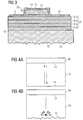
- Fig. 3 shows a shows a resonator comprised in an acoustic wave filter used in a filter device according to a first embodiment of the present invention.
- resonator shown in Fig 3 is a bulk acoustic wave resonator and essentially corresponds to the one described with respect to Fig. 1 of this application.
- Corresponding reference numerals in Fig. 3 denote parts corresponding to those of Fig. 1 .
- the resonator according to Fig. 3 comprises a substrate (10) in which the bottom surface of the substrate (14) has been roughened such that the reflection of an acoustic wave back to the acoustic wave filter is reduced.
- the average height difference between the peaks and the valleys on the roughened bottom surface of the substrate is larger than 0,2 ⁇ , preferably larger than 0,5 ⁇ .
- the average height difference between the peaks and the valleys is larger than 2 ⁇ m, preferably larger than 3 ⁇ m and most preferred larger than 5 ⁇ m.
- the average lateral distance between the peaks and the valleys on the roughened bottom surface of the substrate is smaller than 3 ⁇ , preferably smaller than 2 ⁇ .
- the acoustic mirror two pairs of mirror layers, each pair comprising a layer of a material having a low acoustic impedance (31a, 31c) and a layer of a material having a high acoustic impedance (31b, 31d).
- the number of layers in the acoustic mirror in the filter devices according to the present invention can be varied in order to optimize the mirror stack regarding properties other than the minimization of the reflection of acoustic waves in the substrate.
- a property can be temperature behavior, for instance.
- an acoustic wave filter according to present invention which corresponds to a prior art acoustic wave filter and comprising an identical acoustic mirror but which differs in the feature that the bottom surface of the substrate has been roughened will exhibit less acoustic wave reflection in the substrate than said prior art acoustic wave filter.
- Fig. 4a and b show a schematic comparison of acoustic wave reflection at the bottom surface (14) of a substrate (10) in a prior art filter device (Fig. a) and in a filter device according to the present invention (Fig. b).
- the substrate (10) has a top surface (12) and a bottom surface (14) which has not been roughened.
- the acoustic waves leaking from the acoustic wave filter (40) into the substrate (10) propagate to the bottom surface (14) and are coherently reflected at the smooth bottom surface (14) back up towards the acoustic wave filter (40). This is indicated by the two arrows in Fig. 4a .
- the acoustic waves reflected back towards the acoustic wave filter (40) and cause ripples in the passband of the resonator and consequently in the passband of the filter, which deteriorates it's performance.
- the substrate at certain wavelengths forms an acoustic cavity which further amplifies the deteriorating effects due to the coupling of the reflected waves into the resonator.
- the bottom surface (14) of the substrate (10) has been roughened. Acoustic waves leaking from the acoustic wave filter (40) and reaching the bottom surface (14) are scattered in all directions at the roughened surface. Accordingly, the portion of the acoustic wave that is actually reflected back to the acoustic wave device is reduced. Therefore, the negative effects caused by the reflection of acoustic waves back to the acoustic wave filter are avoided in the filter devices according to the present invention.
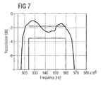
- Fig. 5 to 9 show a comparison of the results of different measurements on filter devices in which the substrate of the filter device has been roughened in accordance with the present invention and the same filter devices without said roughening of the bottom surface of the substrate of the filter device.
- the measurements were carried out on 900 MHz resonators.
- the bottom surface of the substrate was roughened using a conventional plate sander which is normally used in woodwork.
- Figure 5 shows the transmission of a 3.5 step ladder type filter device as a function of the frequency.
- the measurement was carried out using a suitable method to measure the S 21 -component of the scattering matrix of the filter device.
- the definition of the scattering matrix of a filter device is known to the person skilled in the art and can for instance be found in " Zinke, Brunswig; Hochfrequenztechnik 1, 6th edition, Springer Verlag, pages 182 to 185 " the disclosure of which is herewith incorporated by reference.
- the bottom surface of the substrate of the filter device was not roughened prior to the measurement of the transmission.
- the transmission shows numerous ripples in the frequency range from about 920 to 965 MHz. These ripples deteriorate the performance of the filter.
- the transmission shows no such ripples in the passband-section and therefore shows an improved performance as compared to the filter devices in which the bottom surface of the substrate of the filter device is not roughened.
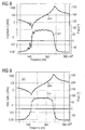
- Figure 8 relates to a filter device without a roughened bottom surface of the substrate of the filter device
- Figure 9 relates to the corresponding filter device in which the bottom surface of the substrate of the filter device is roughened according to the present invention.
- the S 11 -component of the filter device according to the present invention does not exhibit any substantial ripples in both amplitude (Z am ) and phase (z ph ), whereas the performance of the filter device which has not been roughened shows is deteriorated by the ripples in both amplitude (z am ) and phase (z ph ) of the S 11 -component, especially in the range between about 935 MHz to 950 MHz.
Landscapes
- Physics & Mathematics (AREA)
- Acoustics & Sound (AREA)
- Chemical & Material Sciences (AREA)
- Crystallography & Structural Chemistry (AREA)
- Engineering & Computer Science (AREA)
- Manufacturing & Machinery (AREA)
- Piezo-Electric Or Mechanical Vibrators, Or Delay Or Filter Circuits (AREA)
Applications Claiming Priority (1)
| Application Number | Priority Date | Filing Date | Title |
|---|---|---|---|
| PCT/EP2001/012826 WO2003041273A1 (en) | 2001-11-06 | 2001-11-06 | Filter device and method of fabricating a filter device |
Publications (2)
| Publication Number | Publication Date |
|---|---|
| EP1454412A1 EP1454412A1 (en) | 2004-09-08 |
| EP1454412B1 true EP1454412B1 (en) | 2009-10-28 |
Family
ID=8164665
Family Applications (1)
| Application Number | Title | Priority Date | Filing Date |
|---|---|---|---|
| EP01274644A Expired - Lifetime EP1454412B1 (en) | 2001-11-06 | 2001-11-06 | Filter device and method of fabricating a filter device |
Country Status (5)
| Country | Link |
|---|---|
| US (1) | US6943647B2 (enExample) |
| EP (1) | EP1454412B1 (enExample) |
| JP (1) | JP3987036B2 (enExample) |
| DE (1) | DE60140319D1 (enExample) |
| WO (1) | WO2003041273A1 (enExample) |
Families Citing this family (41)
| Publication number | Priority date | Publication date | Assignee | Title |
|---|---|---|---|---|
| EP1540819A1 (en) * | 2002-09-12 | 2005-06-15 | Philips Intellectual Property & Standards GmbH | Bulk acoustic waver resonator with means for suppression of pass-band ripple in bulk acoustic wave filters |
| JP4024741B2 (ja) | 2003-10-20 | 2007-12-19 | 富士通メディアデバイス株式会社 | 圧電薄膜共振子及びフィルタ |
| US7332985B2 (en) * | 2003-10-30 | 2008-02-19 | Avago Technologies Wireless Ip (Singapore) Pte Ltd. | Cavity-less film bulk acoustic resonator (FBAR) devices |
| JP2005260484A (ja) * | 2004-03-10 | 2005-09-22 | Tdk Corp | 圧電共振器およびそれを備えた電子部品 |
| JP2005277454A (ja) * | 2004-03-22 | 2005-10-06 | Tdk Corp | 圧電共振器およびそれを備えた電子部品 |
| US8981876B2 (en) | 2004-11-15 | 2015-03-17 | Avago Technologies General Ip (Singapore) Pte. Ltd. | Piezoelectric resonator structures and electrical filters having frame elements |
| US7791434B2 (en) * | 2004-12-22 | 2010-09-07 | Avago Technologies Wireless Ip (Singapore) Pte. Ltd. | Acoustic resonator performance enhancement using selective metal etch and having a trench in the piezoelectric |
| US7598827B2 (en) | 2006-06-19 | 2009-10-06 | Maxim Integrated Products | Harmonic termination of power amplifiers using BAW filter output matching circuits |
| US7586389B2 (en) * | 2006-06-19 | 2009-09-08 | Maxim Integrated Products, Inc. | Impedance transformation and filter using bulk acoustic wave technology |
| US7706213B2 (en) * | 2006-10-23 | 2010-04-27 | Nancy Ann Winfree | Mechanical filter for sensors |
| US20090053401A1 (en) * | 2007-08-24 | 2009-02-26 | Maxim Integrated Products, Inc. | Piezoelectric deposition for BAW resonators |
| US8512800B2 (en) * | 2007-12-04 | 2013-08-20 | Triquint Semiconductor, Inc. | Optimal acoustic impedance materials for polished substrate coating to suppress passband ripple in BAW resonators and filters |
| DE102008003820B4 (de) * | 2008-01-10 | 2013-01-17 | Epcos Ag | Frontendschaltung |
| US7768364B2 (en) * | 2008-06-09 | 2010-08-03 | Maxim Integrated Products, Inc. | Bulk acoustic resonators with multi-layer electrodes |
| US8030823B2 (en) * | 2009-01-26 | 2011-10-04 | Resonance Semiconductor Corporation | Protected resonator |
| US9735338B2 (en) | 2009-01-26 | 2017-08-15 | Cymatics Laboratories Corp. | Protected resonator |
| US8248185B2 (en) | 2009-06-24 | 2012-08-21 | Avago Technologies Wireless Ip (Singapore) Pte. Ltd. | Acoustic resonator structure comprising a bridge |
| US8902023B2 (en) | 2009-06-24 | 2014-12-02 | Avago Technologies General Ip (Singapore) Pte. Ltd. | Acoustic resonator structure having an electrode with a cantilevered portion |
| JP5617523B2 (ja) * | 2009-12-08 | 2014-11-05 | 株式会社村田製作所 | 積層型圧電薄膜フィルタの製造方法 |
| US9243316B2 (en) | 2010-01-22 | 2016-01-26 | Avago Technologies General Ip (Singapore) Pte. Ltd. | Method of fabricating piezoelectric material with selected c-axis orientation |
| US8796904B2 (en) | 2011-10-31 | 2014-08-05 | Avago Technologies General Ip (Singapore) Pte. Ltd. | Bulk acoustic resonator comprising piezoelectric layer and inverse piezoelectric layer |
| DE102010033867A1 (de) | 2010-08-10 | 2012-02-16 | Epcos Ag | Filteranordnung, Duplexer sowie Verfahren zur Herstellung einer Filteranordnung |
| US8962443B2 (en) | 2011-01-31 | 2015-02-24 | Avago Technologies General Ip (Singapore) Pte. Ltd. | Semiconductor device having an airbridge and method of fabricating the same |
| US9136818B2 (en) | 2011-02-28 | 2015-09-15 | Avago Technologies General Ip (Singapore) Pte. Ltd. | Stacked acoustic resonator comprising a bridge |
| US9203374B2 (en) | 2011-02-28 | 2015-12-01 | Avago Technologies General Ip (Singapore) Pte. Ltd. | Film bulk acoustic resonator comprising a bridge |
| US9154112B2 (en) | 2011-02-28 | 2015-10-06 | Avago Technologies General Ip (Singapore) Pte. Ltd. | Coupled resonator filter comprising a bridge |
| US9048812B2 (en) | 2011-02-28 | 2015-06-02 | Avago Technologies General Ip (Singapore) Pte. Ltd. | Bulk acoustic wave resonator comprising bridge formed within piezoelectric layer |
| US9425764B2 (en) | 2012-10-25 | 2016-08-23 | Avago Technologies General Ip (Singapore) Pte. Ltd. | Accoustic resonator having composite electrodes with integrated lateral features |
| US9148117B2 (en) | 2011-02-28 | 2015-09-29 | Avago Technologies General Ip (Singapore) Pte. Ltd. | Coupled resonator filter comprising a bridge and frame elements |
| US9083302B2 (en) | 2011-02-28 | 2015-07-14 | Avago Technologies General Ip (Singapore) Pte. Ltd. | Stacked bulk acoustic resonator comprising a bridge and an acoustic reflector along a perimeter of the resonator |
| US9484882B2 (en) * | 2013-02-14 | 2016-11-01 | Avago Technologies General Ip (Singapore) Pte. Ltd. | Acoustic resonator having temperature compensation |
| US8575820B2 (en) | 2011-03-29 | 2013-11-05 | Avago Technologies General Ip (Singapore) Pte. Ltd. | Stacked bulk acoustic resonator |
| US9444426B2 (en) | 2012-10-25 | 2016-09-13 | Avago Technologies General Ip (Singapore) Pte. Ltd. | Accoustic resonator having integrated lateral feature and temperature compensation feature |
| US8350445B1 (en) | 2011-06-16 | 2013-01-08 | Avago Technologies Wireless Ip (Singapore) Pte. Ltd. | Bulk acoustic resonator comprising non-piezoelectric layer and bridge |
| US9473106B2 (en) * | 2011-06-21 | 2016-10-18 | Georgia Tech Research Corporation | Thin-film bulk acoustic wave delay line |
| US8922302B2 (en) | 2011-08-24 | 2014-12-30 | Avago Technologies General Ip (Singapore) Pte. Ltd. | Acoustic resonator formed on a pedestal |
| US9254997B2 (en) * | 2013-08-29 | 2016-02-09 | Taiwan Semiconductor Manufacturing Co., Ltd. | CMOS-MEMS integrated flow for making a pressure sensitive transducer |
| US10090820B2 (en) | 2015-07-31 | 2018-10-02 | Qorvo Us, Inc. | Stealth-dicing compatible devices and methods to prevent acoustic backside reflections on acoustic wave devices |
| JP2017046225A (ja) * | 2015-08-27 | 2017-03-02 | 株式会社ディスコ | Bawデバイス及びbawデバイスの製造方法 |
| JP6699927B2 (ja) * | 2016-03-03 | 2020-05-27 | 株式会社ディスコ | Bawデバイス及びbawデバイスの製造方法 |
| JP2020113954A (ja) | 2019-01-16 | 2020-07-27 | 株式会社村田製作所 | 弾性波装置 |
Family Cites Families (16)
| Publication number | Priority date | Publication date | Assignee | Title |
|---|---|---|---|---|
| GB1438777A (en) * | 1973-09-04 | 1976-06-09 | Mullard Ltd | Electromechanical propagation devices and the manufacture thereof |
| FR2261654B1 (enExample) * | 1974-02-15 | 1978-01-06 | Thomson Csf | |
| CA1089544A (en) * | 1976-11-09 | 1980-11-11 | Sadao Takahashi | Elastic surface wave device |
| JPS60126907A (ja) * | 1983-12-12 | 1985-07-06 | Nippon Telegr & Teleph Corp <Ntt> | 単一応答複合圧電振動素子 |
| JPH03165116A (ja) * | 1989-11-22 | 1991-07-17 | Clarion Co Ltd | 弾性表面波装置 |
| US5864261A (en) * | 1994-05-23 | 1999-01-26 | Iowa State University Research Foundation | Multiple layer acoustical structures for thin-film resonator based circuits and systems |
| JPH0897675A (ja) * | 1994-09-28 | 1996-04-12 | Canon Inc | 弾性表面波素子及びその作製方法及びそれを用いた通信装置 |
| US5872493A (en) * | 1997-03-13 | 1999-02-16 | Nokia Mobile Phones, Ltd. | Bulk acoustic wave (BAW) filter having a top portion that includes a protective acoustic mirror |
| US5903087A (en) * | 1997-06-05 | 1999-05-11 | Motorola Inc. | Electrode edge wave patterns for piezoelectric resonator |
| JPH11284481A (ja) * | 1998-03-30 | 1999-10-15 | Murata Mfg Co Ltd | 圧電薄膜振動子およびその製造方法 |
| US6150703A (en) * | 1998-06-29 | 2000-11-21 | Trw Inc. | Lateral mode suppression in semiconductor bulk acoustic resonator (SBAR) devices using tapered electrodes, and electrodes edge damping materials |
| DE19931297A1 (de) * | 1999-07-07 | 2001-01-11 | Philips Corp Intellectual Pty | Volumenwellen-Filter |
| US6603241B1 (en) * | 2000-05-23 | 2003-08-05 | Agere Systems, Inc. | Acoustic mirror materials for acoustic devices |
| KR100398365B1 (ko) * | 2001-06-25 | 2003-09-19 | 삼성전기주식회사 | 폭방향 파동이 억제되는 박막 공진기 |
| US6720844B1 (en) * | 2001-11-16 | 2004-04-13 | Tfr Technologies, Inc. | Coupled resonator bulk acoustic wave filter |
| EP1540819A1 (en) * | 2002-09-12 | 2005-06-15 | Philips Intellectual Property & Standards GmbH | Bulk acoustic waver resonator with means for suppression of pass-band ripple in bulk acoustic wave filters |
-
2001
- 2001-11-06 DE DE60140319T patent/DE60140319D1/de not_active Expired - Lifetime
- 2001-11-06 JP JP2003543190A patent/JP3987036B2/ja not_active Expired - Fee Related
- 2001-11-06 WO PCT/EP2001/012826 patent/WO2003041273A1/en not_active Ceased
- 2001-11-06 EP EP01274644A patent/EP1454412B1/en not_active Expired - Lifetime
-
2004
- 2004-05-06 US US10/840,320 patent/US6943647B2/en not_active Expired - Lifetime
Also Published As
| Publication number | Publication date |
|---|---|
| WO2003041273A1 (en) | 2003-05-15 |
| US6943647B2 (en) | 2005-09-13 |
| DE60140319D1 (de) | 2009-12-10 |
| EP1454412A1 (en) | 2004-09-08 |
| JP3987036B2 (ja) | 2007-10-03 |
| US20040227591A1 (en) | 2004-11-18 |
| JP2005509348A (ja) | 2005-04-07 |
Similar Documents
| Publication | Publication Date | Title |
|---|---|---|
| EP1454412B1 (en) | Filter device and method of fabricating a filter device | |
| KR100799391B1 (ko) | 박막 음향공진기 및 그 제조방법 | |
| EP1196989B1 (en) | Resonator structure and a filter having such a resonator structure | |
| US8525619B1 (en) | Lateral acoustic wave resonator comprising a suspended membrane of low damping resonator material | |
| US7737806B2 (en) | Piezoelectric thin-film resonator and filter | |
| US7138889B2 (en) | Single-port multi-resonator acoustic resonator device | |
| US7463118B2 (en) | Piezoelectric resonator with an efficient all-dielectric Bragg reflector | |
| KR100806504B1 (ko) | 음향 공진기 | |
| US8149500B2 (en) | Bragg mirror and method for making same | |
| US9490770B2 (en) | Acoustic resonator comprising temperature compensating layer and perimeter distributed bragg reflector | |
| CN100440730C (zh) | 电子部件及其制造方法 | |
| CN101026368A (zh) | 膜体声谐振器及其制造方法 | |
| JP2005512442A (ja) | 反射性の改善された音響鏡 | |
| KR20040051539A (ko) | 압전 공진 필터 및 듀플렉서 | |
| JP6556173B2 (ja) | 圧電薄膜共振器、フィルタおよびマルチプレクサ | |
| WO2024040679A1 (zh) | 体声波谐振器及其制作方法、滤波器及电子设备 | |
| CN1862959B (zh) | 压电薄膜谐振器与滤波器 | |
| CN100530955C (zh) | 薄膜压电共振器、滤波器 | |
| US7109637B2 (en) | Thin-film bulk acoustic oscillator and method of manufacturing same | |
| JP7383417B2 (ja) | 弾性波デバイスおよびその製造方法、圧電薄膜共振器、フィルタ並びにマルチプレクサ | |
| CN118631211A (zh) | 谐振器及其制备方法 | |
| JP7641774B2 (ja) | 弾性波デバイス、フィルタおよびマルチプレクサ | |
| CN116208114A (zh) | 一种体声波谐振器及其制备方法 | |
| KR100323802B1 (ko) | 탄성파 소자의 제조방법 및 그에 따라 형성된 탄성파 소자 | |
| WO2024055388A1 (en) | Acoustic resonator |
Legal Events
| Date | Code | Title | Description |
|---|---|---|---|
| PUAI | Public reference made under article 153(3) epc to a published international application that has entered the european phase |
Free format text: ORIGINAL CODE: 0009012 |
|
| 17P | Request for examination filed |
Effective date: 20040428 |
|
| AK | Designated contracting states |
Kind code of ref document: A1 Designated state(s): AT BE CH CY DE DK ES FI FR GB GR IE IT LI LU MC NL PT SE TR |
|
| 17Q | First examination report despatched |
Effective date: 20061116 |
|
| RAP1 | Party data changed (applicant data changed or rights of an application transferred) |
Owner name: AVAGO TECHNOLOGIES WIRELESS IP (SINGAPORE) PTE. LT Owner name: NOKIA CORPORATION |
|
| GRAP | Despatch of communication of intention to grant a patent |
Free format text: ORIGINAL CODE: EPIDOSNIGR1 |
|
| GRAS | Grant fee paid |
Free format text: ORIGINAL CODE: EPIDOSNIGR3 |
|
| GRAA | (expected) grant |
Free format text: ORIGINAL CODE: 0009210 |
|
| AK | Designated contracting states |
Kind code of ref document: B1 Designated state(s): DE |
|
| REF | Corresponds to: |
Ref document number: 60140319 Country of ref document: DE Date of ref document: 20091210 Kind code of ref document: P |
|
| PLBE | No opposition filed within time limit |
Free format text: ORIGINAL CODE: 0009261 |
|
| STAA | Information on the status of an ep patent application or granted ep patent |
Free format text: STATUS: NO OPPOSITION FILED WITHIN TIME LIMIT |
|
| 26N | No opposition filed |
Effective date: 20100729 |
|
| REG | Reference to a national code |
Ref country code: DE Ref legal event code: R082 Ref document number: 60140319 Country of ref document: DE Representative=s name: DILG HAEUSLER SCHINDELMANN PATENTANWALTSGESELL, DE |
|
| REG | Reference to a national code |
Ref country code: DE Ref legal event code: R082 Ref document number: 60140319 Country of ref document: DE Representative=s name: DILG HAEUSLER SCHINDELMANN PATENTANWALTSGESELL, DE Effective date: 20130605 Ref country code: DE Ref legal event code: R081 Ref document number: 60140319 Country of ref document: DE Owner name: NOKIA CORP., FI Free format text: FORMER OWNER: AVAGO TECHNOLOGIES WIRELESS IP , NOKIA CORP., , FI Effective date: 20130605 Ref country code: DE Ref legal event code: R081 Ref document number: 60140319 Country of ref document: DE Owner name: AVAGO TECHNOLOGIES GENERAL IP (SINGAPORE) PTE., SG Free format text: FORMER OWNER: AVAGO TECHNOLOGIES WIRELESS IP , NOKIA CORP., , FI Effective date: 20130605 Ref country code: DE Ref legal event code: R081 Ref document number: 60140319 Country of ref document: DE Owner name: NOKIA CORP., FI Free format text: FORMER OWNERS: AVAGO TECHNOLOGIES WIRELESS IP (SINGAPORE) PTE. LTD., SINGAPORE, SG; NOKIA CORP., 02610 ESPOO, FI Effective date: 20130605 Ref country code: DE Ref legal event code: R081 Ref document number: 60140319 Country of ref document: DE Owner name: AVAGO TECHNOLOGIES GENERAL IP (SINGAPORE) PTE., SG Free format text: FORMER OWNERS: AVAGO TECHNOLOGIES WIRELESS IP (SINGAPORE) PTE. LTD., SINGAPORE, SG; NOKIA CORP., 02610 ESPOO, FI Effective date: 20130605 |
|
| REG | Reference to a national code |
Ref country code: DE Ref legal event code: R081 Ref document number: 60140319 Country of ref document: DE Owner name: NOKIA CORP., FI Free format text: FORMER OWNERS: AVAGO TECHNOLOGIES GENERAL IP (SINGAPORE) PTE. LTD., SINGAPORE, SG; NOKIA CORP., 02610 ESPOO, FI Ref country code: DE Ref legal event code: R081 Ref document number: 60140319 Country of ref document: DE Owner name: AVAGO TECHNOLOGIES INTERNATIONAL SALES PTE. LT, SG Free format text: FORMER OWNERS: AVAGO TECHNOLOGIES GENERAL IP (SINGAPORE) PTE. LTD., SINGAPORE, SG; NOKIA CORP., 02610 ESPOO, FI Ref country code: DE Ref legal event code: R082 Ref document number: 60140319 Country of ref document: DE Representative=s name: DILG, HAEUSLER, SCHINDELMANN PATENTANWALTSGESE, DE Ref country code: DE Ref legal event code: R082 Ref document number: 60140319 Country of ref document: DE Representative=s name: DILG HAEUSLER SCHINDELMANN PATENTANWALTSGESELL, DE |
|
| PGFP | Annual fee paid to national office [announced via postgrant information from national office to epo] |
Ref country code: DE Payment date: 20191127 Year of fee payment: 19 |
|
| REG | Reference to a national code |
Ref country code: DE Ref legal event code: R119 Ref document number: 60140319 Country of ref document: DE |
|
| PG25 | Lapsed in a contracting state [announced via postgrant information from national office to epo] |
Ref country code: DE Free format text: LAPSE BECAUSE OF NON-PAYMENT OF DUE FEES Effective date: 20210601 |