JP3987036B2 - フィルタ装置およびその製造方法 - Google Patents
フィルタ装置およびその製造方法 Download PDFInfo
- Publication number
- JP3987036B2 JP3987036B2 JP2003543190A JP2003543190A JP3987036B2 JP 3987036 B2 JP3987036 B2 JP 3987036B2 JP 2003543190 A JP2003543190 A JP 2003543190A JP 2003543190 A JP2003543190 A JP 2003543190A JP 3987036 B2 JP3987036 B2 JP 3987036B2
- Authority
- JP
- Japan
- Prior art keywords
- substrate
- filter
- acoustic
- elastic
- filter device
- Prior art date
- Legal status (The legal status is an assumption and is not a legal conclusion. Google has not performed a legal analysis and makes no representation as to the accuracy of the status listed.)
- Expired - Fee Related
Links
- 238000004519 manufacturing process Methods 0.000 title claims description 10
- 239000000758 substrate Substances 0.000 claims description 94
- 239000000463 material Substances 0.000 claims description 23
- 238000000034 method Methods 0.000 claims description 21
- 239000013078 crystal Substances 0.000 claims description 13
- XUIMIQQOPSSXEZ-UHFFFAOYSA-N Silicon Chemical compound [Si] XUIMIQQOPSSXEZ-UHFFFAOYSA-N 0.000 claims description 7
- 229910052710 silicon Inorganic materials 0.000 claims description 7
- 239000010703 silicon Substances 0.000 claims description 7
- 238000005530 etching Methods 0.000 claims description 3
- 238000005498 polishing Methods 0.000 claims description 2
- 238000001039 wet etching Methods 0.000 claims description 2
- 239000010410 layer Substances 0.000 description 57
- 230000005540 biological transmission Effects 0.000 description 9
- 230000000694 effects Effects 0.000 description 8
- 238000010897 surface acoustic wave method Methods 0.000 description 8
- 238000007788 roughening Methods 0.000 description 7
- 239000010409 thin film Substances 0.000 description 6
- 238000010586 diagram Methods 0.000 description 5
- 238000005259 measurement Methods 0.000 description 5
- 238000009792 diffusion process Methods 0.000 description 4
- 238000005516 engineering process Methods 0.000 description 4
- 239000011521 glass Substances 0.000 description 4
- 239000010931 gold Substances 0.000 description 4
- 239000011159 matrix material Substances 0.000 description 4
- PIGFYZPCRLYGLF-UHFFFAOYSA-N Aluminum nitride Chemical compound [Al]#N PIGFYZPCRLYGLF-UHFFFAOYSA-N 0.000 description 3
- 229910004298 SiO 2 Inorganic materials 0.000 description 3
- XLOMVQKBTHCTTD-UHFFFAOYSA-N Zinc monoxide Chemical compound [Zn]=O XLOMVQKBTHCTTD-UHFFFAOYSA-N 0.000 description 3
- WFKWXMTUELFFGS-UHFFFAOYSA-N tungsten Chemical compound [W] WFKWXMTUELFFGS-UHFFFAOYSA-N 0.000 description 3
- 229910052721 tungsten Inorganic materials 0.000 description 3
- 239000010937 tungsten Substances 0.000 description 3
- JBRZTFJDHDCESZ-UHFFFAOYSA-N AsGa Chemical compound [As]#[Ga] JBRZTFJDHDCESZ-UHFFFAOYSA-N 0.000 description 2
- 229910001218 Gallium arsenide Inorganic materials 0.000 description 2
- VYPSYNLAJGMNEJ-UHFFFAOYSA-N Silicium dioxide Chemical compound O=[Si]=O VYPSYNLAJGMNEJ-UHFFFAOYSA-N 0.000 description 2
- 239000005083 Zinc sulfide Substances 0.000 description 2
- 229910052782 aluminium Inorganic materials 0.000 description 2
- XAGFODPZIPBFFR-UHFFFAOYSA-N aluminium Chemical compound [Al] XAGFODPZIPBFFR-UHFFFAOYSA-N 0.000 description 2
- 230000006866 deterioration Effects 0.000 description 2
- PCHJSUWPFVWCPO-UHFFFAOYSA-N gold Chemical compound [Au] PCHJSUWPFVWCPO-UHFFFAOYSA-N 0.000 description 2
- 229910052737 gold Inorganic materials 0.000 description 2
- 238000002955 isolation Methods 0.000 description 2
- 229910021420 polycrystalline silicon Inorganic materials 0.000 description 2
- 229920000642 polymer Polymers 0.000 description 2
- 229920005591 polysilicon Polymers 0.000 description 2
- 230000008569 process Effects 0.000 description 2
- 229910052814 silicon oxide Inorganic materials 0.000 description 2
- 239000000126 substance Substances 0.000 description 2
- 229910052984 zinc sulfide Inorganic materials 0.000 description 2
- ZOKXTWBITQBERF-UHFFFAOYSA-N Molybdenum Chemical compound [Mo] ZOKXTWBITQBERF-UHFFFAOYSA-N 0.000 description 1
- 239000006061 abrasive grain Substances 0.000 description 1
- 238000010521 absorption reaction Methods 0.000 description 1
- 230000008901 benefit Effects 0.000 description 1
- 230000015556 catabolic process Effects 0.000 description 1
- 229910010293 ceramic material Inorganic materials 0.000 description 1
- 230000008859 change Effects 0.000 description 1
- 238000006243 chemical reaction Methods 0.000 description 1
- 238000004891 communication Methods 0.000 description 1
- 238000006731 degradation reaction Methods 0.000 description 1
- 230000000593 degrading effect Effects 0.000 description 1
- 230000001419 dependent effect Effects 0.000 description 1
- 238000000227 grinding Methods 0.000 description 1
- 238000009413 insulation Methods 0.000 description 1
- DNHVXYDGZKWYNU-UHFFFAOYSA-N lead;hydrate Chemical compound O.[Pb] DNHVXYDGZKWYNU-UHFFFAOYSA-N 0.000 description 1
- 230000007246 mechanism Effects 0.000 description 1
- 229910052750 molybdenum Inorganic materials 0.000 description 1
- 239000011733 molybdenum Substances 0.000 description 1
- 238000007517 polishing process Methods 0.000 description 1
- 230000008092 positive effect Effects 0.000 description 1
- 230000001902 propagating effect Effects 0.000 description 1
- 239000011241 protective layer Substances 0.000 description 1
- 230000004044 response Effects 0.000 description 1
- 238000004544 sputter deposition Methods 0.000 description 1
- 230000003746 surface roughness Effects 0.000 description 1
- DRDVZXDWVBGGMH-UHFFFAOYSA-N zinc;sulfide Chemical compound [S-2].[Zn+2] DRDVZXDWVBGGMH-UHFFFAOYSA-N 0.000 description 1
Images


Classifications
-
- H—ELECTRICITY
- H03—ELECTRONIC CIRCUITRY
- H03H—IMPEDANCE NETWORKS, e.g. RESONANT CIRCUITS; RESONATORS
- H03H9/00—Networks comprising electromechanical or electro-acoustic devices; Electromechanical resonators
- H03H9/15—Constructional features of resonators consisting of piezoelectric or electrostrictive material
- H03H9/17—Constructional features of resonators consisting of piezoelectric or electrostrictive material having a single resonator
- H03H9/171—Constructional features of resonators consisting of piezoelectric or electrostrictive material having a single resonator implemented with thin-film techniques, i.e. of the film bulk acoustic resonator [FBAR] type
- H03H9/172—Means for mounting on a substrate, i.e. means constituting the material interface confining the waves to a volume
- H03H9/175—Acoustic mirrors
-
- H—ELECTRICITY
- H03—ELECTRONIC CIRCUITRY
- H03H—IMPEDANCE NETWORKS, e.g. RESONANT CIRCUITS; RESONATORS
- H03H3/00—Apparatus or processes specially adapted for the manufacture of impedance networks, resonating circuits, resonators
- H03H3/007—Apparatus or processes specially adapted for the manufacture of impedance networks, resonating circuits, resonators for the manufacture of electromechanical resonators or networks
- H03H3/02—Apparatus or processes specially adapted for the manufacture of impedance networks, resonating circuits, resonators for the manufacture of electromechanical resonators or networks for the manufacture of piezoelectric or electrostrictive resonators or networks
-
- H—ELECTRICITY
- H03—ELECTRONIC CIRCUITRY
- H03H—IMPEDANCE NETWORKS, e.g. RESONANT CIRCUITS; RESONATORS
- H03H9/00—Networks comprising electromechanical or electro-acoustic devices; Electromechanical resonators
- H03H9/02—Details
- H03H9/02007—Details of bulk acoustic wave devices
- H03H9/02047—Treatment of substrates
- H03H9/02055—Treatment of substrates of the surface including the back surface
-
- H—ELECTRICITY
- H03—ELECTRONIC CIRCUITRY
- H03H—IMPEDANCE NETWORKS, e.g. RESONANT CIRCUITS; RESONATORS
- H03H9/00—Networks comprising electromechanical or electro-acoustic devices; Electromechanical resonators
- H03H9/02—Details
- H03H9/02007—Details of bulk acoustic wave devices
- H03H9/02086—Means for compensation or elimination of undesirable effects
- H03H9/0211—Means for compensation or elimination of undesirable effects of reflections
-
- H—ELECTRICITY
- H03—ELECTRONIC CIRCUITRY
- H03H—IMPEDANCE NETWORKS, e.g. RESONANT CIRCUITS; RESONATORS
- H03H9/00—Networks comprising electromechanical or electro-acoustic devices; Electromechanical resonators
- H03H9/46—Filters
- H03H9/54—Filters comprising resonators of piezo-electric or electrostrictive material
- H03H9/58—Multiple crystal filters
- H03H9/582—Multiple crystal filters implemented with thin-film techniques
- H03H9/583—Multiple crystal filters implemented with thin-film techniques comprising a plurality of piezoelectric layers acoustically coupled
- H03H9/585—Stacked Crystal Filters [SCF]
-
- H—ELECTRICITY
- H03—ELECTRONIC CIRCUITRY
- H03H—IMPEDANCE NETWORKS, e.g. RESONANT CIRCUITS; RESONATORS
- H03H9/00—Networks comprising electromechanical or electro-acoustic devices; Electromechanical resonators
- H03H9/46—Filters
- H03H9/54—Filters comprising resonators of piezo-electric or electrostrictive material
- H03H9/58—Multiple crystal filters
- H03H9/582—Multiple crystal filters implemented with thin-film techniques
- H03H9/586—Means for mounting to a substrate, i.e. means constituting the material interface confining the waves to a volume
- H03H9/589—Acoustic mirrors
-
- Y—GENERAL TAGGING OF NEW TECHNOLOGICAL DEVELOPMENTS; GENERAL TAGGING OF CROSS-SECTIONAL TECHNOLOGIES SPANNING OVER SEVERAL SECTIONS OF THE IPC; TECHNICAL SUBJECTS COVERED BY FORMER USPC CROSS-REFERENCE ART COLLECTIONS [XRACs] AND DIGESTS
- Y10—TECHNICAL SUBJECTS COVERED BY FORMER USPC
- Y10T—TECHNICAL SUBJECTS COVERED BY FORMER US CLASSIFICATION
- Y10T29/00—Metal working
- Y10T29/42—Piezoelectric device making
Description
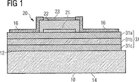
(a)上面および下面を有する基板
(b)基板の上面に接触する少なくとも1つの弾性波フィルタ
このとき、基板の下面は、弾性波の弾性波フィルタへの反射を低減させるために、粗くなっている。
Claims (16)
- (a)上面(12)および下面(14)を有する基板(10)と、
(b)共振周波数が0.5〜5GHzである少なくとも1つの弾性バルク波共振器を含んだ、少なくとも1つの弾性バルク波(BAW)フィルタ(20)とを含み、
上記弾性バルク波(BAW)フィルタ(20)は、基板(10)の上面(12)に接触しており、
上記基板(10)の下面(14)が、弾性波の弾性波フィルタ(20)への反射を低減させるためにでこぼこになっている、フィルタ装置。 - でこぼこにした基板の下面における突出部と窪みとの平均高度差が、0.2λよりも大きく、好ましくは0.5λよりも大きい、請求項1に記載のフィルタ装置。
- 上記でこぼこにした基板の下面における突出部と窪みとの平均横方向距離が、3λよりも小さく、好ましくは2λよりも小さい、請求項1または2に記載のフィルタ装置。
- 上記弾性波フィルタが、少なくとも1つの積層型結晶フィルタ(SCF)を含んだ弾性バルク波(BAW)フィルタである、請求項1〜3のいずれか1項に記載のフィルタ装置。
- 上記弾性波フィルタは、少なくとも1つの音響ミラーをさらに含んでいる、請求項1〜4のいずれか1項に記載のフィルタ装置。
- 上記音響ミラーは、弾性バルク波共振器または積層型結晶フィルタと、基板の上面(12)との間に配置されている、請求項5に記載のフィルタ装置。
- 上記音響ミラーは、ミラー層を2組のみ含んでおり、この各組のミラー層が、高い音響インピーダンスを有する材料からなる層と、低い音響インピーダンスを有する材料からなる層とを含んでおり、双方の組のミラー層は、高い音響インピーダンスを有する材料からなる2つの層が、低い音響インピーダンスを有する材料からなる1つの層によって隔てられて配置されている、請求項5または6に記載のフィルタ装置。
- 上記基板がシリコン基板である、請求項1〜7のいずれか1項に記載のフィルタ装置。
- フィルタ装置の製造方法であって、
(a)上記上面(12)および下面(14)を有する基板(10)を準備するステップと、
(b)上記基板(10)の上面(12)に、共振周波数が0.5〜5GHzの弾性バルク波共振器を少なくとも1つ含む弾性バルク波フィルタ(20)を少なくとも1つ形成するステップと、
(c)上記弾性バルク波フィルタ(20)への弾性波の反射が低減するように、基板(10)の下面(14)をでこぼこにするステップとを含んだ、製造方法。 - 上記した基板(10)の下面(14)をでこぼこにするステップ(c)を、基板を薄くすると同時に実施する、請求項9に記載の方法。
- 上記の下面(14)をでこぼこにするステップは、機械を用いて実施される、請求項9または10に記載の方法。
- 上記の下面をでこぼこにするステップは、研磨によって実施される、請求項9〜11のいずれか1項に記載の方法。
- 上記の下面(14)をでこぼこにするステップは、エッチング、好ましくはウェットエッチングによって実施される、請求項9または10に記載の方法。
- 上記弾性波フィルタは、少なくとも1つの積層型結晶フィルタ(SCF)を含んだ弾性バルク波(BAW)フィルタである、請求項9〜13のいずれか1項に記載の方法。
- 上記ステップ(b)では、基板(10)の上面(12)と、弾性波フィルタにおける弾性バルク波共振器または積層型結晶フィルタ(SCF)との間に配置される音響ミラーを形成する、請求項9〜14のいずれか1項に記載の方法。
- 上記基板(10)がシリコン基板である、請求項9〜15のいずれか1項に記載の方法。
Applications Claiming Priority (1)
| Application Number | Priority Date | Filing Date | Title |
|---|---|---|---|
| PCT/EP2001/012826 WO2003041273A1 (en) | 2001-11-06 | 2001-11-06 | Filter device and method of fabricating a filter device |
Publications (3)
| Publication Number | Publication Date |
|---|---|
| JP2005509348A JP2005509348A (ja) | 2005-04-07 |
| JP2005509348A5 JP2005509348A5 (ja) | 2007-04-05 |
| JP3987036B2 true JP3987036B2 (ja) | 2007-10-03 |
Family
ID=8164665
Family Applications (1)
| Application Number | Title | Priority Date | Filing Date |
|---|---|---|---|
| JP2003543190A Expired - Fee Related JP3987036B2 (ja) | 2001-11-06 | 2001-11-06 | フィルタ装置およびその製造方法 |
Country Status (5)
| Country | Link |
|---|---|
| US (1) | US6943647B2 (ja) |
| EP (1) | EP1454412B1 (ja) |
| JP (1) | JP3987036B2 (ja) |
| DE (1) | DE60140319D1 (ja) |
| WO (1) | WO2003041273A1 (ja) |
Cited By (1)
| Publication number | Priority date | Publication date | Assignee | Title |
|---|---|---|---|---|
| US11146237B2 (en) | 2019-01-16 | 2021-10-12 | Murata Manufacturing Co., Ltd. | Acoustic wave device |
Families Citing this family (40)
| Publication number | Priority date | Publication date | Assignee | Title |
|---|---|---|---|---|
| US20060043507A1 (en) * | 2002-09-12 | 2006-03-02 | Hans Lobl | Bulk acoustic wave resonator with means for suppression of pass-band ripple in bulk acoustic wave filters |
| JP4024741B2 (ja) | 2003-10-20 | 2007-12-19 | 富士通メディアデバイス株式会社 | 圧電薄膜共振子及びフィルタ |
| US7332985B2 (en) * | 2003-10-30 | 2008-02-19 | Avago Technologies Wireless Ip (Singapore) Pte Ltd. | Cavity-less film bulk acoustic resonator (FBAR) devices |
| JP2005260484A (ja) * | 2004-03-10 | 2005-09-22 | Tdk Corp | 圧電共振器およびそれを備えた電子部品 |
| JP2005277454A (ja) * | 2004-03-22 | 2005-10-06 | Tdk Corp | 圧電共振器およびそれを備えた電子部品 |
| US8981876B2 (en) | 2004-11-15 | 2015-03-17 | Avago Technologies General Ip (Singapore) Pte. Ltd. | Piezoelectric resonator structures and electrical filters having frame elements |
| US7791434B2 (en) * | 2004-12-22 | 2010-09-07 | Avago Technologies Wireless Ip (Singapore) Pte. Ltd. | Acoustic resonator performance enhancement using selective metal etch and having a trench in the piezoelectric |
| US7586389B2 (en) * | 2006-06-19 | 2009-09-08 | Maxim Integrated Products, Inc. | Impedance transformation and filter using bulk acoustic wave technology |
| US7598827B2 (en) * | 2006-06-19 | 2009-10-06 | Maxim Integrated Products | Harmonic termination of power amplifiers using BAW filter output matching circuits |
| US7706213B2 (en) * | 2006-10-23 | 2010-04-27 | Nancy Ann Winfree | Mechanical filter for sensors |
| US20090053401A1 (en) * | 2007-08-24 | 2009-02-26 | Maxim Integrated Products, Inc. | Piezoelectric deposition for BAW resonators |
| US8512800B2 (en) | 2007-12-04 | 2013-08-20 | Triquint Semiconductor, Inc. | Optimal acoustic impedance materials for polished substrate coating to suppress passband ripple in BAW resonators and filters |
| DE102008003820B4 (de) * | 2008-01-10 | 2013-01-17 | Epcos Ag | Frontendschaltung |
| US7768364B2 (en) * | 2008-06-09 | 2010-08-03 | Maxim Integrated Products, Inc. | Bulk acoustic resonators with multi-layer electrodes |
| US9735338B2 (en) | 2009-01-26 | 2017-08-15 | Cymatics Laboratories Corp. | Protected resonator |
| US8030823B2 (en) * | 2009-01-26 | 2011-10-04 | Resonance Semiconductor Corporation | Protected resonator |
| US8248185B2 (en) | 2009-06-24 | 2012-08-21 | Avago Technologies Wireless Ip (Singapore) Pte. Ltd. | Acoustic resonator structure comprising a bridge |
| US8902023B2 (en) | 2009-06-24 | 2014-12-02 | Avago Technologies General Ip (Singapore) Pte. Ltd. | Acoustic resonator structure having an electrode with a cantilevered portion |
| JP5617523B2 (ja) * | 2009-12-08 | 2014-11-05 | 株式会社村田製作所 | 積層型圧電薄膜フィルタの製造方法 |
| US8796904B2 (en) | 2011-10-31 | 2014-08-05 | Avago Technologies General Ip (Singapore) Pte. Ltd. | Bulk acoustic resonator comprising piezoelectric layer and inverse piezoelectric layer |
| US9243316B2 (en) | 2010-01-22 | 2016-01-26 | Avago Technologies General Ip (Singapore) Pte. Ltd. | Method of fabricating piezoelectric material with selected c-axis orientation |
| DE102010033867A1 (de) | 2010-08-10 | 2012-02-16 | Epcos Ag | Filteranordnung, Duplexer sowie Verfahren zur Herstellung einer Filteranordnung |
| US8962443B2 (en) | 2011-01-31 | 2015-02-24 | Avago Technologies General Ip (Singapore) Pte. Ltd. | Semiconductor device having an airbridge and method of fabricating the same |
| US9048812B2 (en) | 2011-02-28 | 2015-06-02 | Avago Technologies General Ip (Singapore) Pte. Ltd. | Bulk acoustic wave resonator comprising bridge formed within piezoelectric layer |
| US9203374B2 (en) | 2011-02-28 | 2015-12-01 | Avago Technologies General Ip (Singapore) Pte. Ltd. | Film bulk acoustic resonator comprising a bridge |
| US9136818B2 (en) | 2011-02-28 | 2015-09-15 | Avago Technologies General Ip (Singapore) Pte. Ltd. | Stacked acoustic resonator comprising a bridge |
| US9083302B2 (en) | 2011-02-28 | 2015-07-14 | Avago Technologies General Ip (Singapore) Pte. Ltd. | Stacked bulk acoustic resonator comprising a bridge and an acoustic reflector along a perimeter of the resonator |
| US9154112B2 (en) | 2011-02-28 | 2015-10-06 | Avago Technologies General Ip (Singapore) Pte. Ltd. | Coupled resonator filter comprising a bridge |
| US9425764B2 (en) | 2012-10-25 | 2016-08-23 | Avago Technologies General Ip (Singapore) Pte. Ltd. | Accoustic resonator having composite electrodes with integrated lateral features |
| US9148117B2 (en) | 2011-02-28 | 2015-09-29 | Avago Technologies General Ip (Singapore) Pte. Ltd. | Coupled resonator filter comprising a bridge and frame elements |
| US9484882B2 (en) * | 2013-02-14 | 2016-11-01 | Avago Technologies General Ip (Singapore) Pte. Ltd. | Acoustic resonator having temperature compensation |
| US8575820B2 (en) | 2011-03-29 | 2013-11-05 | Avago Technologies General Ip (Singapore) Pte. Ltd. | Stacked bulk acoustic resonator |
| US9444426B2 (en) | 2012-10-25 | 2016-09-13 | Avago Technologies General Ip (Singapore) Pte. Ltd. | Accoustic resonator having integrated lateral feature and temperature compensation feature |
| US8350445B1 (en) | 2011-06-16 | 2013-01-08 | Avago Technologies Wireless Ip (Singapore) Pte. Ltd. | Bulk acoustic resonator comprising non-piezoelectric layer and bridge |
| US9473106B2 (en) * | 2011-06-21 | 2016-10-18 | Georgia Tech Research Corporation | Thin-film bulk acoustic wave delay line |
| US8922302B2 (en) | 2011-08-24 | 2014-12-30 | Avago Technologies General Ip (Singapore) Pte. Ltd. | Acoustic resonator formed on a pedestal |
| US9254997B2 (en) * | 2013-08-29 | 2016-02-09 | Taiwan Semiconductor Manufacturing Co., Ltd. | CMOS-MEMS integrated flow for making a pressure sensitive transducer |
| US10090820B2 (en) | 2015-07-31 | 2018-10-02 | Qorvo Us, Inc. | Stealth-dicing compatible devices and methods to prevent acoustic backside reflections on acoustic wave devices |
| JP2017046225A (ja) * | 2015-08-27 | 2017-03-02 | 株式会社ディスコ | Bawデバイス及びbawデバイスの製造方法 |
| JP6699927B2 (ja) * | 2016-03-03 | 2020-05-27 | 株式会社ディスコ | Bawデバイス及びbawデバイスの製造方法 |
Family Cites Families (16)
| Publication number | Priority date | Publication date | Assignee | Title |
|---|---|---|---|---|
| GB1438777A (en) * | 1973-09-04 | 1976-06-09 | Mullard Ltd | Electromechanical propagation devices and the manufacture thereof |
| FR2261654B1 (ja) * | 1974-02-15 | 1978-01-06 | Thomson Csf | |
| CA1089544A (en) * | 1976-11-09 | 1980-11-11 | Sadao Takahashi | Elastic surface wave device |
| JPS60126907A (ja) * | 1983-12-12 | 1985-07-06 | Nippon Telegr & Teleph Corp <Ntt> | 単一応答複合圧電振動素子 |
| JPH03165116A (ja) * | 1989-11-22 | 1991-07-17 | Clarion Co Ltd | 弾性表面波装置 |
| US5864261A (en) * | 1994-05-23 | 1999-01-26 | Iowa State University Research Foundation | Multiple layer acoustical structures for thin-film resonator based circuits and systems |
| JPH0897675A (ja) * | 1994-09-28 | 1996-04-12 | Canon Inc | 弾性表面波素子及びその作製方法及びそれを用いた通信装置 |
| US5872493A (en) * | 1997-03-13 | 1999-02-16 | Nokia Mobile Phones, Ltd. | Bulk acoustic wave (BAW) filter having a top portion that includes a protective acoustic mirror |
| US5903087A (en) * | 1997-06-05 | 1999-05-11 | Motorola Inc. | Electrode edge wave patterns for piezoelectric resonator |
| JPH11284481A (ja) * | 1998-03-30 | 1999-10-15 | Murata Mfg Co Ltd | 圧電薄膜振動子およびその製造方法 |
| US6150703A (en) * | 1998-06-29 | 2000-11-21 | Trw Inc. | Lateral mode suppression in semiconductor bulk acoustic resonator (SBAR) devices using tapered electrodes, and electrodes edge damping materials |
| DE19931297A1 (de) * | 1999-07-07 | 2001-01-11 | Philips Corp Intellectual Pty | Volumenwellen-Filter |
| US6603241B1 (en) * | 2000-05-23 | 2003-08-05 | Agere Systems, Inc. | Acoustic mirror materials for acoustic devices |
| KR100398365B1 (ko) * | 2001-06-25 | 2003-09-19 | 삼성전기주식회사 | 폭방향 파동이 억제되는 박막 공진기 |
| US6720844B1 (en) * | 2001-11-16 | 2004-04-13 | Tfr Technologies, Inc. | Coupled resonator bulk acoustic wave filter |
| US20060043507A1 (en) * | 2002-09-12 | 2006-03-02 | Hans Lobl | Bulk acoustic wave resonator with means for suppression of pass-band ripple in bulk acoustic wave filters |
-
2001
- 2001-11-06 JP JP2003543190A patent/JP3987036B2/ja not_active Expired - Fee Related
- 2001-11-06 DE DE60140319T patent/DE60140319D1/de not_active Expired - Lifetime
- 2001-11-06 EP EP01274644A patent/EP1454412B1/en not_active Expired - Lifetime
- 2001-11-06 WO PCT/EP2001/012826 patent/WO2003041273A1/en active Application Filing
-
2004
- 2004-05-06 US US10/840,320 patent/US6943647B2/en not_active Expired - Lifetime
Cited By (1)
| Publication number | Priority date | Publication date | Assignee | Title |
|---|---|---|---|---|
| US11146237B2 (en) | 2019-01-16 | 2021-10-12 | Murata Manufacturing Co., Ltd. | Acoustic wave device |
Also Published As
| Publication number | Publication date |
|---|---|
| JP2005509348A (ja) | 2005-04-07 |
| DE60140319D1 (de) | 2009-12-10 |
| EP1454412B1 (en) | 2009-10-28 |
| WO2003041273A1 (en) | 2003-05-15 |
| US6943647B2 (en) | 2005-09-13 |
| US20040227591A1 (en) | 2004-11-18 |
| EP1454412A1 (en) | 2004-09-08 |
Similar Documents
| Publication | Publication Date | Title |
|---|---|---|
| JP3987036B2 (ja) | フィルタ装置およびその製造方法 | |
| US11699988B2 (en) | Resonator and method for manufacturing the same | |
| US20200336127A1 (en) | Hybrid structure for a surface acoustic wave device | |
| US7884527B2 (en) | Piezoelectric thin-film resonator and filter using the same | |
| KR100799391B1 (ko) | 박막 음향공진기 및 그 제조방법 | |
| US7463118B2 (en) | Piezoelectric resonator with an efficient all-dielectric Bragg reflector | |
| US6534900B2 (en) | Piezoresonator | |
| KR100806504B1 (ko) | 음향 공진기 | |
| JP3592276B2 (ja) | 音響共振器および音響共振器の組立方法 | |
| US7719388B2 (en) | Resonator operating with bulk acoustic waves | |
| KR102449355B1 (ko) | 음향 공진기 및 그의 제조 방법 | |
| US7109637B2 (en) | Thin-film bulk acoustic oscillator and method of manufacturing same | |
| WO2024040679A1 (zh) | 体声波谐振器及其制作方法、滤波器及电子设备 | |
| JP6831256B2 (ja) | 圧電薄膜共振器、フィルタおよびマルチプレクサ | |
| KR100323802B1 (ko) | 탄성파 소자의 제조방법 및 그에 따라 형성된 탄성파 소자 | |
| JP2022189419A (ja) | 圧電薄膜共振器、フィルタ、およびマルチプレクサ | |
| TW202215778A (zh) | 體聲波共振器 | |
| JP2001156583A (ja) | 圧電共振子 | |
| KR20220148456A (ko) | 박막 벌크 음향 공진기 | |
| CN116418311A (zh) | 体声波谐振器 | |
| CN117439572A (zh) | 声表面波谐振装置及形成方法、滤波装置 | |
| JP2005093465A (ja) | 薄膜キャパシタ、圧電フィルタおよびその製造方法、ならびに分波器、通信機 |
Legal Events
| Date | Code | Title | Description |
|---|---|---|---|
| A977 | Report on retrieval |
Free format text: JAPANESE INTERMEDIATE CODE: A971007 Effective date: 20061026 |
|
| A131 | Notification of reasons for refusal |
Free format text: JAPANESE INTERMEDIATE CODE: A131 Effective date: 20061107 |
|
| A524 | Written submission of copy of amendment under article 19 pct |
Free format text: JAPANESE INTERMEDIATE CODE: A524 Effective date: 20070206 |
|
| TRDD | Decision of grant or rejection written | ||
| A01 | Written decision to grant a patent or to grant a registration (utility model) |
Free format text: JAPANESE INTERMEDIATE CODE: A01 Effective date: 20070612 |
|
| A61 | First payment of annual fees (during grant procedure) |
Free format text: JAPANESE INTERMEDIATE CODE: A61 Effective date: 20070711 |
|
| R150 | Certificate of patent or registration of utility model |
Ref document number: 3987036 Country of ref document: JP Free format text: JAPANESE INTERMEDIATE CODE: R150 Free format text: JAPANESE INTERMEDIATE CODE: R150 |
|
| FPAY | Renewal fee payment (event date is renewal date of database) |
Free format text: PAYMENT UNTIL: 20100720 Year of fee payment: 3 |
|
| FPAY | Renewal fee payment (event date is renewal date of database) |
Free format text: PAYMENT UNTIL: 20100720 Year of fee payment: 3 |
|
| S111 | Request for change of ownership or part of ownership |
Free format text: JAPANESE INTERMEDIATE CODE: R313113 |
|
| FPAY | Renewal fee payment (event date is renewal date of database) |
Free format text: PAYMENT UNTIL: 20100720 Year of fee payment: 3 |
|
| R360 | Written notification for declining of transfer of rights |
Free format text: JAPANESE INTERMEDIATE CODE: R360 |
|
| FPAY | Renewal fee payment (event date is renewal date of database) |
Free format text: PAYMENT UNTIL: 20100720 Year of fee payment: 3 |
|
| R370 | Written measure of declining of transfer procedure |
Free format text: JAPANESE INTERMEDIATE CODE: R370 |
|
| FPAY | Renewal fee payment (event date is renewal date of database) |
Free format text: PAYMENT UNTIL: 20100720 Year of fee payment: 3 |
|
| S111 | Request for change of ownership or part of ownership |
Free format text: JAPANESE INTERMEDIATE CODE: R313117 |
|
| FPAY | Renewal fee payment (event date is renewal date of database) |
Free format text: PAYMENT UNTIL: 20100720 Year of fee payment: 3 |
|
| R350 | Written notification of registration of transfer |
Free format text: JAPANESE INTERMEDIATE CODE: R350 |
|
| FPAY | Renewal fee payment (event date is renewal date of database) |
Free format text: PAYMENT UNTIL: 20110720 Year of fee payment: 4 |
|
| R250 | Receipt of annual fees |
Free format text: JAPANESE INTERMEDIATE CODE: R250 |
|
| FPAY | Renewal fee payment (event date is renewal date of database) |
Free format text: PAYMENT UNTIL: 20110720 Year of fee payment: 4 |
|
| FPAY | Renewal fee payment (event date is renewal date of database) |
Free format text: PAYMENT UNTIL: 20120720 Year of fee payment: 5 |
|
| R250 | Receipt of annual fees |
Free format text: JAPANESE INTERMEDIATE CODE: R250 |
|
| FPAY | Renewal fee payment (event date is renewal date of database) |
Free format text: PAYMENT UNTIL: 20120720 Year of fee payment: 5 |
|
| FPAY | Renewal fee payment (event date is renewal date of database) |
Free format text: PAYMENT UNTIL: 20130720 Year of fee payment: 6 |
|
| R250 | Receipt of annual fees |
Free format text: JAPANESE INTERMEDIATE CODE: R250 |
|
| R250 | Receipt of annual fees |
Free format text: JAPANESE INTERMEDIATE CODE: R250 |
|
| S111 | Request for change of ownership or part of ownership |
Free format text: JAPANESE INTERMEDIATE CODE: R313111 |
|
| R360 | Written notification for declining of transfer of rights |
Free format text: JAPANESE INTERMEDIATE CODE: R360 |
|
| R370 | Written measure of declining of transfer procedure |
Free format text: JAPANESE INTERMEDIATE CODE: R370 |
|
| S111 | Request for change of ownership or part of ownership |
Free format text: JAPANESE INTERMEDIATE CODE: R313115 |
|
| R350 | Written notification of registration of transfer |
Free format text: JAPANESE INTERMEDIATE CODE: R350 |
|
| R250 | Receipt of annual fees |
Free format text: JAPANESE INTERMEDIATE CODE: R250 |
|
| R250 | Receipt of annual fees |
Free format text: JAPANESE INTERMEDIATE CODE: R250 |
|
| R250 | Receipt of annual fees |
Free format text: JAPANESE INTERMEDIATE CODE: R250 |
|
| R250 | Receipt of annual fees |
Free format text: JAPANESE INTERMEDIATE CODE: R250 |
|
| R250 | Receipt of annual fees |
Free format text: JAPANESE INTERMEDIATE CODE: R250 |
|
| R250 | Receipt of annual fees |
Free format text: JAPANESE INTERMEDIATE CODE: R250 |
|
| R250 | Receipt of annual fees |
Free format text: JAPANESE INTERMEDIATE CODE: R250 |
|
| LAPS | Cancellation because of no payment of annual fees |