EP1443654A2 - Verfahren und Schaltung zur Wandlung eines analogen Istsignals in ein digitales Sollsignal - Google Patents
Verfahren und Schaltung zur Wandlung eines analogen Istsignals in ein digitales Sollsignal Download PDFInfo
- Publication number
- EP1443654A2 EP1443654A2 EP03027196A EP03027196A EP1443654A2 EP 1443654 A2 EP1443654 A2 EP 1443654A2 EP 03027196 A EP03027196 A EP 03027196A EP 03027196 A EP03027196 A EP 03027196A EP 1443654 A2 EP1443654 A2 EP 1443654A2
- Authority
- EP
- European Patent Office
- Prior art keywords
- digital
- signal
- analog
- comparator
- output
- Prior art date
- Legal status (The legal status is an assumption and is not a legal conclusion. Google has not performed a legal analysis and makes no representation as to the accuracy of the status listed.)
- Granted
Links
Images
Classifications
-
- H—ELECTRICITY
- H03—ELECTRONIC CIRCUITRY
- H03M—CODING; DECODING; CODE CONVERSION IN GENERAL
- H03M1/00—Analogue/digital conversion; Digital/analogue conversion
- H03M1/12—Analogue/digital converters
- H03M1/48—Servo-type converters
-
- H—ELECTRICITY
- H03—ELECTRONIC CIRCUITRY
- H03M—CODING; DECODING; CODE CONVERSION IN GENERAL
- H03M1/00—Analogue/digital conversion; Digital/analogue conversion
- H03M1/12—Analogue/digital converters
- H03M1/34—Analogue value compared with reference values
- H03M1/38—Analogue value compared with reference values sequentially only, e.g. successive approximation type
- H03M1/46—Analogue value compared with reference values sequentially only, e.g. successive approximation type with digital/analogue converter for supplying reference values to converter
Definitions
- the invention relates to a method and a circuit for converting an analog Actual signal into a digital target signal according to the preamble of patent claim 1.
- RF systems with RF (radio frequency) amplifiers including detectors, e.g. RF detectors or current sensors, for monitoring the transmit and receive operations known.
- a detected video signal is an image of the received one rf pulse.
- These rf pulses are used by analog comparators against a reference threshold supervised. The output of these comparators is analyzed and the result usually forwarded via serial interfaces for further processing.
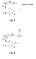
- the analog comparators K are usually programmable comparators K, which generate the reference threshold, the analog target signal AS S , internally by means of a built-in digital / analog converter D / A.
- the corresponding digital values DS S for the analog desired signal AS S are stored in a known storage medium SP, for example an EPROM, and are written into the corresponding comparator input 1 depending on the operating mode of the comparator K.
- the analog actual signal S I is fed to the other comparator input 2. At the comparator output A it can be determined whether the actual signal I S is larger or smaller than the target signal AS S. (Fig. 1)
- the rf power to be monitored is e.g. one RF power meter (so-called peak power analyzer) measured.
- the detected voltage can be measured at the detector.
- the latter is usually done with an oscilloscope, measuring the voltage at the output pin of the respective comparator.
- the object of the invention is a simple, fast and as automatic as possible Specify a method for converting an analog actual signal into a digital target signal with which an adaptive calibration of detectors is possible. Another The task is to create a circuit for performing this method.
- the digital input signal supplied to the digital / analog converter depending on the output signal at the comparator output of the comparator in a predeterminable number of iteration steps between a predeterminable lower and a predeterminable upper threshold adapted to the weighing process, the one fed to the digital / analog converter in each case digital input signal corresponds to the digital target signal in which the analog actual signal is converted.
- the reference threshold becomes dependent the number of predeterminable iteration steps is processed in binary form.
- the number of iteration steps of the bit length with which the digital target signal is specified shall be.
- the accuracy can thus of the target signal and thus the reference threshold.
- the analog actual signal with an 8-bit resolution simulated.
- the simulation is done bit by bit according to the known weighing method, in which the voltage applied to the comparator in several Steps are approximated successively.
- Such a process is in digital technology in addition to the parallel method and the counting method, a known method the implementation of A / D and / or D / A converters.
- An advantage of the method according to the invention is that it can be checked using an oscilloscope and its external adaptation can be dispensed with. Also more time and costly conversion measures are not necessary with the invention Method.
- the calibration can e.g. simply and quickly without any modifications be carried out in a climate chamber.
- the analog actual signal comprises one Burst with several pulses of predefinable pulse length.
- the pulse length can e.g. in the area of only a few ⁇ s.
- a burst can be any number of pulses, (e.g. 268 pulses).
- the successive pulses can e.g. RF power transistors due to from warming to a change in the actual signal during the burst come (so-called burst droop).
- burst droop When measurements have turned out to be surprising It turns out that regular bursts are the same forever Pulses in the burst result in the same conditions (constant actual value).
- the actual signal on the comparator for a Predeterminable reference pulse viewed from the burst.
- this reference pulse advantageously the signal value corresponding to the pulse center in Comparator processed.
- the generated digital target signal can be falsified by EMC interference (e.g. so-called spikes).
- the digital desired signal is verified in two further iteration steps, burst n + 9 and burst n + 10.
- a predeterminable signal value for example 10% of the typical maximum value, is subtracted from the digital target signal obtained. This only takes place if the digital target signal previously had a correspondingly high value.
- an overshoot must occur. If this is not the case, the setpoint obtained for this cycle is discarded. The corresponding result is recorded in a status bit.
- a predefinable signal value for example 10% of the typical maximum value, is added to the target signal beforehand if the value is less than the maximum value.
- the setpoints thus obtained are indicated by an existing bus system from the device under test to an external test computer. Depending on requirements and data, this calculates data from other sources (e.g. PeakPowerMeter) individual setpoints come as operating thresholds. The values those operating thresholds are then programmed in the test device's eproms.
- sources e.g. PeakPowerMeter
- the respective comparator monitors the detected pulse power in operational operation against a reference value which was previously derived from the corresponding Eprom has been loaded into the input register of the DA converter in the comparator.
- the circuit comprises a comparator K with two input ports 1, 2 and an output port A and a digital / analog converter D / A with a digital input port D E and an analog output port D A.
- the analog output gate D A is connected to an input gate 1 of the comparator K.
- the other input gate 2 of the comparator K is supplied with the analog actual signal I S to be converted.
- the output gate A of the comparator K is connected to an electronic component KV for generating a digital target signal DS S , which is fed to the digital input gate D E of the digital / analog converter D / A.
- the electronic component KV is designed such that it generates the digital target signal DS S using the weighing method.
- the digital target signal DS S generated by the electronic component KV can also be supplied to further components (not shown) for further processing.
Landscapes
- Engineering & Computer Science (AREA)
- Theoretical Computer Science (AREA)
- Analogue/Digital Conversion (AREA)
Abstract
Description
Im letzten Schritt (Burst n+10) wird dem Sollsignal zuvor ein vorgebbarer Signalwert, z.B. 10% des typischen Maximalwertes aufaddiert, wenn der Wert kleiner als der Maximalwert ist. Beim Vergleich von aktuellem Istsignal (am Referenzpuls) mit dem um die Differenz vermindertem Sollsignal muss eine Unterschreitung auftreten. Ist dies nicht der Fall, wird der gewonnene Sollwert für diesen Zyklus verworfen. In einem Statusbit wird das entsprechende Ergebnis festgehalten.
Claims (6)
- Verfahren zur Wandlung eines analogen Istsignals (SI) in ein digitales Sollsignal (DSS) mittels eines zwei Eingangstore (1, 2) und ein Ausgangstor (A) aufweisenden Komparators (K) und eines integrierten Digital/Analog-Wandlers (D/A), wobei dem einen Eingangstor (1, 2) des Komparators (K) das zu wandelnde analoge Istsignal (SI) und dem anderen Eingangstor (2, 1) des Komparators (K) das analoge Ausgangssignal (ASS) des Digital/Analog-Wandlers (D/A) zugeführt wird, dadurch gekennzeichnet, dass das dem Digital/Analog-Wandler (D/A) zugeführte digitale Eingangssignal (DSS) in Abhängigkeit vom dem am Komparatorausgang (A) anliegende Ausgangssignal des Komparators (K) in einer vorgebbaren Anzahl von Iterationsschritten zwischen einer vorgebbaren unteren und einer vorgebbaren oberen Schwelle nach dem Wägeverfahren angepasst wird, wobei das dem Digital/Analog-Wandler (D/A) jeweils zugeführte digitale Eingangssignal (DSS) dem digitalen Sollsignal (DSS) entspricht in welches das analoge Istsignal (SI) gewandelt wird.
- Verfahren nach Anspruch 1, dadurch gekennzeichnet, dass das analoge Istsignal (SI) einem Burst umfassend einer vorgebbaren Anzahl von Pulsen entspricht.
- Verfahren nach Anspruch 2, dadurch gekennzeichnet, dass dem Komparator (K) ein vorgebbarer Referenzpuls aus dem Burst zugeführt wird und dass von diesem Referenzpuls im Komparator (K) der der Pulsmitte entsprechende Signalwert verarbeitet wird.
- Verfahren nach einem der vorangehenden Ansprüche, dadurch gekennzeichnet, dass die Zahl der vorgebbaren Iterationsschritte der Bitlänge entspricht, mit der das digitale Sollsignal (DSS) angegeben wird.
- Verfahren nach einem der vorangehenden Ansprüchen, dadurch gekennzeichnet, dass das digitale Sollsignal (DSS) verifiziert wird, derart, dass in einem ersten weiteren Iterationsschritt von dem analogen Istsignal (SI) ein vorgebbarer Signalwert abgezogen wird, welches dann dem einen Eingangstor (2, 1) des Komparators (K) zugeführt wird und welches mittels des am Ausgang (A) anliegende Ausgangssignals des Komparators (K) auf Unterschreitung des am anderen Eingangstor (1, 2) des Komparators (K) anliegende, im Digital-/Analog-Wandler (D/A) aus dem zu verifizierenden digitalen Sollsignal (DSS) erzeugte analoge Ausgangssignal (ASS) des Digital-Analog-Wandlers (D/A) geprüft wird und dass in einem zweiten weiteren Iterationsschritt zu dem analogen Istsignal (SI) ein entsprechend vorgebbarer Signalwert addiert wird, welches dann dem einen Eingangstor (2, 1) des Komparators zugeführt wird und welches mittels des am Ausgangstor (A) anliegenden Ausgangssignals des Komparators (K) auf Überschreitung des am anderen Eingangstor (1, 2) des Komparators (K) anliegende, im Digital-/Analog-Wandler (D/A) aus dem zu verifizierende digitalen Sollsignal (DSS) erzeugte analoge Ausgangssignal (ASS) des Digital-Analog-Wandlers (D/A) geprüft wird, wobei das digitale Sollsignal (DSS) als korrekt angenommen wird, wenn der Prüfschritt im ersten und der Prüfschritt im zweiten weiteren Iterationsschritt erfolgreich war.
- Schaltung zur Durchführung eines Verfahrens nach einem der vorangehenden Ansprüche umfassend einen Komparator (K) mit zwei Eingangstoren (1, 2) und einem Ausgangstor (A) sowie einem Digital/Analog-Wandler (D/A) mit einem digitalen Eingangstor (DE) und einem analogen Ausgangstor (DA) , wobei das analoge Ausgangstor (DA) mit einem Eingangstor (1, 2) des Komparators (K) verbunden ist und das zu wandelnde analoge Istsignal (IS) dem anderen Eingangstor (2, 1) des Komparators (K) zugeführt ist und wobei das analoge Ausgangstor (A) des Komparators (K) mit einem elektronischen Bauteil (KV) zur Erzeugung eines digitalen Sollsignals (DSS) verbunden ist, welches dem digitalen Eingangstor (DE) des Digital/Analog-Wandlers (D/A) zugeführt ist.
Applications Claiming Priority (2)
| Application Number | Priority Date | Filing Date | Title |
|---|---|---|---|
| DE10303347 | 2003-01-29 | ||
| DE10303347A DE10303347B4 (de) | 2003-01-29 | 2003-01-29 | Verfahren und Schaltung zur Wandlung eines analogen Istsignals in ein digitales Sollsignal |
Publications (3)
| Publication Number | Publication Date |
|---|---|
| EP1443654A2 true EP1443654A2 (de) | 2004-08-04 |
| EP1443654A3 EP1443654A3 (de) | 2006-07-19 |
| EP1443654B1 EP1443654B1 (de) | 2008-05-28 |
Family
ID=32603011
Family Applications (1)
| Application Number | Title | Priority Date | Filing Date |
|---|---|---|---|
| EP03027196A Expired - Lifetime EP1443654B1 (de) | 2003-01-29 | 2003-11-27 | Verfahren und Schaltung zur Wandlung eines analogen Istsignals in ein digitales Sollsignal |
Country Status (4)
| Country | Link |
|---|---|
| US (1) | US6958724B2 (de) |
| EP (1) | EP1443654B1 (de) |
| DE (2) | DE10303347B4 (de) |
| ES (1) | ES2305394T3 (de) |
Families Citing this family (1)
| Publication number | Priority date | Publication date | Assignee | Title |
|---|---|---|---|---|
| FI121101B (fi) * | 2007-01-22 | 2010-06-30 | Abb Oy | Laite analogisen virta- tai jännitesignaalin tuottamiseksi |
Family Cites Families (77)
| Publication number | Priority date | Publication date | Assignee | Title |
|---|---|---|---|---|
| US426652A (en) * | 1890-04-29 | Method of manufacturing axles | ||
| JPS5014015B1 (de) * | 1969-10-18 | 1975-05-24 | ||
| NL151955B (nl) * | 1970-06-10 | 1977-01-17 | Leidsche Apparatenfabriek Nv | Selecteerinrichting voor aan een zijde open holle voorwerpen. |
| US3722656A (en) * | 1971-06-23 | 1973-03-27 | Rexham Corp | System for handling and accumulating articles |
| US3734263A (en) * | 1971-07-02 | 1973-05-22 | A Dirks | Revolvable station for processing a movable procession of factory-work pieces such as animal carcasses |
| US3815723A (en) * | 1971-11-05 | 1974-06-11 | Cutler Hammer Inc | Method and apparatus for transferring and storing articles |
| IT968102B (it) * | 1972-12-18 | 1974-03-20 | Acma Spa | Apparato per ordinare a passo oggetti provenienti disordina tamente da una linea erogatrice e per trasferirli quindi ad una linea ricevitrice |
| FR2225363B1 (de) * | 1973-04-10 | 1977-09-02 | Remy & Cie E P | |
| US4029194A (en) * | 1974-05-13 | 1977-06-14 | Pemco, Inc. | Automatic indexing and transferring apparatus |
| US4040302A (en) * | 1975-01-03 | 1977-08-09 | Mitsubishi Jukogyo Kabushiki Kaisha | Chain drive for a transfer machine |
| US4033403A (en) * | 1975-09-17 | 1977-07-05 | Seaton Engineering Company | Synchronizing velocity and position control |
| US4044886A (en) * | 1975-12-29 | 1977-08-30 | Sender Wilfred E | System for handling structural members |
| FR2417455A1 (fr) * | 1978-02-20 | 1979-09-14 | Arenco Decoufle Sa Fse | Dispositif pour transferer transversalement des objets cylindriques en forme de tiges, se deplacant longitudinalement |
| US4340137A (en) * | 1978-03-27 | 1982-07-20 | Opcon, Inc. | Cant movement and aligning mechanism |
| IT1188972B (it) * | 1980-12-12 | 1988-01-28 | Gd Spa | Dispositivo di trasferimento per articoli a forma di barretta |
| US4450950A (en) * | 1981-05-12 | 1984-05-29 | Eastman Kodak Company | Work piece transfer mechanism |
| FR2524436B1 (fr) * | 1982-04-02 | 1985-09-27 | Nantaise Biscuiterie | Dispositif regulateur de transfert de produits solides identiques entre des machines amont et aval de vitesses differentes |
| DE3276991D1 (en) * | 1982-12-28 | 1987-09-17 | Ibm | Analog-digital converter |
| US4524858A (en) * | 1983-05-24 | 1985-06-25 | Maxey Carl W | Edger transport and position apparatus |
| JPS6034311A (ja) * | 1983-07-28 | 1985-02-21 | 日本たばこ産業株式会社 | 停止待機運転制御式集積包装機の製品受渡搬送装置 |
| US4667809A (en) * | 1983-10-19 | 1987-05-26 | Trimmer Machine Co., Inc. | Apparatus for aligning signatures |
| US4585126A (en) * | 1983-10-28 | 1986-04-29 | Sunkist Growers, Inc. | Method and apparatus for high speed processing of fruit or the like |
| US4768109A (en) * | 1983-12-24 | 1988-08-30 | Victor Company Of Japan, Ltd. | Video signal recording and/or reproducing apparatus |
| US4603770A (en) * | 1984-01-18 | 1986-08-05 | Hartness Thomas Signor | Rake conveyor apparatus |
| IT1181265B (it) * | 1984-12-06 | 1987-09-23 | Gd Spa | Dispositivo per il trasferimento di articoli a forma di barretta |
| GB2187120B (en) * | 1986-02-27 | 1990-01-04 | Honda Motor Co Ltd | System for installing parts on workpiece |
| JPH0761019B2 (ja) * | 1986-06-19 | 1995-06-28 | 日本電気株式会社 | アナログ・デイジタル変換器 |
| US4898373A (en) * | 1986-07-03 | 1990-02-06 | Newsome John R | High speed signature manipulating apparatus |
| US4869637A (en) * | 1986-08-27 | 1989-09-26 | Bud Antle, Inc. | Plant transfer mechanism |
| DE3763553D1 (de) * | 1986-09-02 | 1990-08-09 | Siemens Ag | Analog-digital-umsetzer nach dem waegeverfahren. |
| US5110249A (en) * | 1986-10-23 | 1992-05-05 | Innotec Group, Inc. | Transport system for inline vacuum processing |
| US4759439A (en) * | 1987-01-29 | 1988-07-26 | Dominion Chain Inc. | Drive mechanism |
| US4813528A (en) * | 1987-02-06 | 1989-03-21 | Dominion Chain Inc. | Conveyor loading system |
| US4765453A (en) * | 1987-04-27 | 1988-08-23 | Westinghouse Electric Corp. | Pellet-press-to-sintering-boat nuclear fuel pellet loading system |
| US4831382A (en) * | 1987-05-26 | 1989-05-16 | American Telephone And Telegraph Company | Analog-to-digital converter with adaptable quantizing levels |
| DE3724693C2 (de) * | 1987-07-25 | 1996-10-17 | Bosch Gmbh Robert | Verfahren und Vorrichtung zum Überführen von Gegenständen in eine Fördereinrichtung einer Verpackungsmaschine |
| US4777470A (en) * | 1987-09-28 | 1988-10-11 | Burr-Brown Corporation | High speed successive approximation register in analog-to-digital converter |
| US4830180A (en) * | 1988-01-15 | 1989-05-16 | Key Technology, Inc. | Article inspection and stabilizing system |
| US5028927A (en) * | 1988-09-02 | 1991-07-02 | Sharp Kabushiki Kaisha | Signal processing device for analogue to digital conversion |
| US5086909A (en) * | 1988-09-23 | 1992-02-11 | Powell Machinery, Inc. | Gentle handling of fruit during weight sizing and other operations |
| US5057841A (en) * | 1989-07-07 | 1991-10-15 | U.S. Philips Corporation | Analog-to-digital converter |
| US5135102A (en) * | 1989-09-19 | 1992-08-04 | Quipp, Incorporated | Sorting conveyor |
| JPH03106721A (ja) * | 1989-09-21 | 1991-05-07 | Mitsubishi Electric Corp | 縦型ウエーハ搬送装置 |
| US6425331B1 (en) * | 1990-07-09 | 2002-07-30 | Sawgrass Systems, Inc. | Permanent heat activated printing process |
| DE4111899A1 (de) * | 1991-04-12 | 1992-10-15 | Bosch Gmbh Robert | Vorrichtung zum transportieren von gegenstaenden in eine foerdereinrichtung einer verpackungsmaschine |
| US5099896A (en) * | 1991-04-24 | 1992-03-31 | Harvey Industries, Inc | Rotary board pick/store/place method and apparatus |
| IT1252458B (it) * | 1991-07-29 | 1995-06-16 | Gd Spa | Metodo per il trasferimento di prodotti fra trasportatori dotati di moto continuo |
| US5231926A (en) * | 1991-10-11 | 1993-08-03 | Sequa Corporation | Apparatus and method for substantially reducing can spacing and speed to match chain pins |
| US5123518A (en) * | 1991-12-12 | 1992-06-23 | Pfaff Ernest H | Apparatus for properly positioning vials |
| JPH05336534A (ja) * | 1992-06-04 | 1993-12-17 | Sony Corp | レベル検出回路 |
| US5320208A (en) * | 1992-07-02 | 1994-06-14 | Utica Enterprises, Inc. | Reciprocating lift mechanism |
| CA2074789C (en) * | 1992-07-28 | 1995-12-05 | Joel W. Jones | Precision guided transfer fixture |
| US5207309A (en) * | 1992-08-18 | 1993-05-04 | Simpkin Steven W | Concomitant motion control device |
| US5269119A (en) * | 1993-03-12 | 1993-12-14 | Ossid Corporation | Linearly reciprocating conveyor apparatus |
| US5515050A (en) * | 1993-07-06 | 1996-05-07 | Advanced Micro Devices, Inc. | Apparatus and method for asynchronous successive approximation |
| US5653327A (en) * | 1994-10-21 | 1997-08-05 | Electrocom Gard Ltd. | Inserter device and a method for transposing a stream of products using the same |
| GB9503783D0 (en) * | 1995-02-24 | 1995-04-12 | Fujitsu Ltd | Analog-to-digital converters |
| US5628614A (en) * | 1995-03-16 | 1997-05-13 | Douglas Machine Limited Liability Company | Continuous motion stacking apparatus and methods |
| US5667056A (en) * | 1995-06-06 | 1997-09-16 | Sears, Roebuck And Co. | Hanger transport system |
| US5617944A (en) * | 1995-06-15 | 1997-04-08 | Valiant Machine & Tool, Inc. | Shuttle transfer assembly |
| US5558198A (en) * | 1995-09-18 | 1996-09-24 | Juarez; Ramiro O. | Band transportation system |
| IT1285453B1 (it) * | 1996-01-25 | 1998-06-08 | Ima Spa | Metodo ed apparecchiatura per il prelievo e l'impilaggio di prodotti alimentari in file multiple e per il convogliamento delle pile di |
| US6036426A (en) * | 1996-01-26 | 2000-03-14 | Creative Design Corporation | Wafer handling method and apparatus |
| US5823319A (en) * | 1996-05-10 | 1998-10-20 | The Buschman Company | Control system for the drop-out zone of a constant speed accumulating conveyor |
| DE19712161C2 (de) * | 1997-03-22 | 1999-04-15 | Lucent Tech Network Sys Gmbh | Vorrichtung zur Pulsformung von Hochfrequenzsignalen |
| US6183186B1 (en) * | 1997-08-29 | 2001-02-06 | Daitron, Inc. | Wafer handling system and method |
| JP3546217B2 (ja) * | 1997-11-21 | 2004-07-21 | 株式会社ダイフク | 物品移載装置 |
| US6163291A (en) * | 1998-01-21 | 2000-12-19 | Texas Instruments Incorporated | Successive approximation analog to digital converter with bit error correction |
| JP3446598B2 (ja) * | 1998-03-23 | 2003-09-16 | 株式会社村田製作所 | チップ部品の移載装置 |
| US6351231B1 (en) * | 1999-12-23 | 2002-02-26 | Analog Devices, Inc. | Successive approximation analogue-to-digital converter |
| EP1150432B1 (de) * | 2000-04-27 | 2004-11-17 | STMicroelectronics S.r.l. | Analog-Digital-Wandler mit schrittweiser Annäherung und entsprechendes Betriebsverfahren |
| US6329938B1 (en) * | 2000-06-15 | 2001-12-11 | Adaptec, Inc. | Programmable analog-to-digital converter with bit conversion optimization |
| JP2002026731A (ja) * | 2000-07-04 | 2002-01-25 | Mitsubishi Electric Corp | 逐次比較型a/dコンバータ |
| US6581750B1 (en) * | 2000-07-26 | 2003-06-24 | Carl Strutz & Co., Inc. | Method and apparatus for changing the orientation of workpieces about an angled axis for a decorator |
| US6608582B2 (en) * | 2001-06-29 | 2003-08-19 | Intel Corporation | A/D conversion using a variable offset comparator |
| DE10139488C1 (de) | 2001-08-10 | 2003-01-02 | Infineon Technologies Ag | Analog/Digital-Wandler |
| US6511065B1 (en) * | 2001-08-28 | 2003-01-28 | Heidelberger Druckmaschinen Ag | Method for transferring signatures and gripper assembly for a matched velocity transfer device |
-
2003
- 2003-01-29 DE DE10303347A patent/DE10303347B4/de not_active Expired - Fee Related
- 2003-11-27 ES ES03027196T patent/ES2305394T3/es not_active Expired - Lifetime
- 2003-11-27 DE DE50309913T patent/DE50309913D1/de not_active Expired - Lifetime
- 2003-11-27 EP EP03027196A patent/EP1443654B1/de not_active Expired - Lifetime
-
2004
- 2004-01-27 US US10/764,489 patent/US6958724B2/en not_active Expired - Lifetime
Also Published As
| Publication number | Publication date |
|---|---|
| EP1443654A3 (de) | 2006-07-19 |
| DE10303347A1 (de) | 2004-08-19 |
| EP1443654B1 (de) | 2008-05-28 |
| US6958724B2 (en) | 2005-10-25 |
| DE10303347B4 (de) | 2010-04-29 |
| US20040239547A1 (en) | 2004-12-02 |
| ES2305394T3 (es) | 2008-11-01 |
| DE50309913D1 (de) | 2008-07-10 |
Similar Documents
| Publication | Publication Date | Title |
|---|---|---|
| DE112021006159T5 (de) | Systeme, verfahren und vorrichtungen zum hochgeschwindigkeits-eingangs/ ausgangs-margin-test | |
| DE112016003066T5 (de) | Eingebauter Selbsttest für einen ADC | |
| DE69733829T2 (de) | Amplitudenkalibrierung eines messinstruments | |
| WO2014057020A1 (de) | Verfahren und system zur bestimmung von streuparametern eines frequenzumsetzenden messobjekts | |
| DE10236900B4 (de) | Verfahren zum Durchführen eines Bitfehlerratentests und Bitfehlerratentestsystem | |
| DE19700513A1 (de) | Mit CAD-Daten verknüpftes Halbleiterprüfsystem | |
| DE112007003743T5 (de) | Verfahren und Systeme zum Steuern von Schaltern in Leistungsreglern/Leistungverstärkern | |
| EP3649476B1 (de) | Vorrichtung und verfahren zum überprüfen einer funktionsfähigkeit eines systemwiderstands eines batteriesystems | |
| DE69623683T2 (de) | Delta-T-Messschaltung | |
| DE102010006052A1 (de) | Verfahren und Systeme zum Testen von Digital-Analogwandler/Verstärkerschaltungen | |
| DE102018114091B4 (de) | Verfahren zur Datenwandlung, bei denen ein Zustand basierend auf zeitpunktzugehörigen Linearitätsparametern bestimmt wird, sowie Vorrichtungen und Systeme zur Datenwandlung, eingerichtet, einen Zustand basierend auf zeitpunktzugehörigen Linearitätsparametern zu bestimmen | |
| EP1443654B1 (de) | Verfahren und Schaltung zur Wandlung eines analogen Istsignals in ein digitales Sollsignal | |
| DE112004002615T5 (de) | Verfahren zur Kalibrierung eines Zeitsteuertakts | |
| DE102018114092B4 (de) | Verfahren, Vorrichtungen und Systeme zur Überwachung von Datenwandlern welche einen Kalibrierungsdatensatz aufweisen | |
| DE102014202678A1 (de) | Verfahren und Vorrichtung zum Erkennen eines Kurzschlusses an einer PWM-Treiberschaltung | |
| DE102006052842A1 (de) | Jittermessvorrichtung, Jittermessverfahren und Prüfvorrichtung | |
| DE2623892A1 (de) | Verfahren und einrichtung zum bewerten von ultraschall-signalen | |
| DE102007011817B4 (de) | Verfahren und Vorrichtung zum Lokalisieren von Fehlern auf elektronischen Leiterplatten mit kapazitivem Sensor | |
| DE102004052246B3 (de) | Halbleiterbauelement, Anordnung und Verfahren zur Charakterisierung eines Prüfgerätes für Halbleiterbauelemente | |
| DE60300141T2 (de) | Aufspüren eines Signalübergangs | |
| DE102006052843A1 (de) | Jittermessvorrichtung, Jittermessverfahren und Prüfvorrichtung | |
| DE102006018207B4 (de) | Verfahren zum Testen einer A/D-Wandlerschaltung | |
| DE102024200772B3 (de) | Verfahren zum bestimmen eines zustands eines prüfstands, computerpogramm, steuervorrichtung und prüfstand | |
| EP2190121A1 (de) | Mehrkanaliger AD-Wandler | |
| DE102015114211A1 (de) | Sensorschaltung zum Auswerten eines Sensorsignals |
Legal Events
| Date | Code | Title | Description |
|---|---|---|---|
| PUAI | Public reference made under article 153(3) epc to a published international application that has entered the european phase |
Free format text: ORIGINAL CODE: 0009012 |
|
| AK | Designated contracting states |
Kind code of ref document: A2 Designated state(s): AT BE BG CH CY CZ DE DK EE ES FI FR GB GR HU IE IT LI LU MC NL PT RO SE SI SK TR |
|
| AX | Request for extension of the european patent |
Extension state: AL LT LV MK |
|
| PUAL | Search report despatched |
Free format text: ORIGINAL CODE: 0009013 |
|
| AK | Designated contracting states |
Kind code of ref document: A3 Designated state(s): AT BE BG CH CY CZ DE DK EE ES FI FR GB GR HU IE IT LI LU MC NL PT RO SE SI SK TR |
|
| AX | Request for extension of the european patent |
Extension state: AL LT LV MK |
|
| 17P | Request for examination filed |
Effective date: 20061222 |
|
| 17Q | First examination report despatched |
Effective date: 20070119 |
|
| AKX | Designation fees paid |
Designated state(s): DE ES FR GB IT |
|
| 17Q | First examination report despatched |
Effective date: 20070119 |
|
| GRAP | Despatch of communication of intention to grant a patent |
Free format text: ORIGINAL CODE: EPIDOSNIGR1 |
|
| GRAS | Grant fee paid |
Free format text: ORIGINAL CODE: EPIDOSNIGR3 |
|
| GRAA | (expected) grant |
Free format text: ORIGINAL CODE: 0009210 |
|
| AK | Designated contracting states |
Kind code of ref document: B1 Designated state(s): DE ES FR GB IT |
|
| REG | Reference to a national code |
Ref country code: GB Ref legal event code: FG4D Free format text: NOT ENGLISH |
|
| REF | Corresponds to: |
Ref document number: 50309913 Country of ref document: DE Date of ref document: 20080710 Kind code of ref document: P |
|
| REG | Reference to a national code |
Ref country code: ES Ref legal event code: FG2A Ref document number: 2305394 Country of ref document: ES Kind code of ref document: T3 |
|
| PLBE | No opposition filed within time limit |
Free format text: ORIGINAL CODE: 0009261 |
|
| STAA | Information on the status of an ep patent application or granted ep patent |
Free format text: STATUS: NO OPPOSITION FILED WITHIN TIME LIMIT |
|
| 26N | No opposition filed |
Effective date: 20090303 |
|
| REG | Reference to a national code |
Ref country code: DE Ref legal event code: R081 Ref document number: 50309913 Country of ref document: DE Owner name: AIRBUS DEFENCE AND SPACE GMBH, DE Free format text: FORMER OWNER: EADS DEUTSCHLAND GMBH, 85521 OTTOBRUNN, DE Effective date: 20140916 Ref country code: DE Ref legal event code: R081 Ref document number: 50309913 Country of ref document: DE Owner name: AIRBUS DS ELECTRONICS AND BORDER SECURITY GMBH, DE Free format text: FORMER OWNER: EADS DEUTSCHLAND GMBH, 85521 OTTOBRUNN, DE Effective date: 20140916 Ref country code: DE Ref legal event code: R081 Ref document number: 50309913 Country of ref document: DE Owner name: HENSOLDT SENSORS GMBH, DE Free format text: FORMER OWNER: EADS DEUTSCHLAND GMBH, 85521 OTTOBRUNN, DE Effective date: 20140916 |
|
| REG | Reference to a national code |
Ref country code: FR Ref legal event code: PLFP Year of fee payment: 13 |
|
| REG | Reference to a national code |
Ref country code: DE Ref legal event code: R081 Ref document number: 50309913 Country of ref document: DE Owner name: AIRBUS DS ELECTRONICS AND BORDER SECURITY GMBH, DE Free format text: FORMER OWNER: AIRBUS DEFENCE AND SPACE GMBH, 85521 OTTOBRUNN, DE Ref country code: DE Ref legal event code: R081 Ref document number: 50309913 Country of ref document: DE Owner name: HENSOLDT SENSORS GMBH, DE Free format text: FORMER OWNER: AIRBUS DEFENCE AND SPACE GMBH, 85521 OTTOBRUNN, DE |
|
| REG | Reference to a national code |
Ref country code: FR Ref legal event code: PLFP Year of fee payment: 14 |
|
| PGFP | Annual fee paid to national office [announced via postgrant information from national office to epo] |
Ref country code: FR Payment date: 20161118 Year of fee payment: 14 Ref country code: GB Payment date: 20161122 Year of fee payment: 14 Ref country code: DE Payment date: 20161121 Year of fee payment: 14 |
|
| PGFP | Annual fee paid to national office [announced via postgrant information from national office to epo] |
Ref country code: ES Payment date: 20161114 Year of fee payment: 14 Ref country code: IT Payment date: 20161123 Year of fee payment: 14 |
|
| REG | Reference to a national code |
Ref country code: DE Ref legal event code: R082 Ref document number: 50309913 Country of ref document: DE Representative=s name: LIFETECH IP SPIES & BEHRNDT PATENTANWAELTE PAR, DE Ref country code: DE Ref legal event code: R081 Ref document number: 50309913 Country of ref document: DE Owner name: HENSOLDT SENSORS GMBH, DE Free format text: FORMER OWNER: AIRBUS DS ELECTRONICS AND BORDER SECURITY GMBH, 82024 TAUFKIRCHEN, DE |
|
| REG | Reference to a national code |
Ref country code: DE Ref legal event code: R119 Ref document number: 50309913 Country of ref document: DE |
|
| GBPC | Gb: european patent ceased through non-payment of renewal fee |
Effective date: 20171127 |
|
| REG | Reference to a national code |
Ref country code: FR Ref legal event code: ST Effective date: 20180731 |
|
| PG25 | Lapsed in a contracting state [announced via postgrant information from national office to epo] |
Ref country code: FR Free format text: LAPSE BECAUSE OF NON-PAYMENT OF DUE FEES Effective date: 20171130 Ref country code: DE Free format text: LAPSE BECAUSE OF NON-PAYMENT OF DUE FEES Effective date: 20180602 Ref country code: IT Free format text: LAPSE BECAUSE OF NON-PAYMENT OF DUE FEES Effective date: 20171127 |
|
| PG25 | Lapsed in a contracting state [announced via postgrant information from national office to epo] |
Ref country code: GB Free format text: LAPSE BECAUSE OF NON-PAYMENT OF DUE FEES Effective date: 20171127 |
|
| PG25 | Lapsed in a contracting state [announced via postgrant information from national office to epo] |
Ref country code: ES Free format text: LAPSE BECAUSE OF NON-PAYMENT OF DUE FEES Effective date: 20171128 |