EP1432528B1 - Method for edge sealing barrier films - Google Patents
Method for edge sealing barrier films Download PDFInfo
- Publication number
- EP1432528B1 EP1432528B1 EP02766338A EP02766338A EP1432528B1 EP 1432528 B1 EP1432528 B1 EP 1432528B1 EP 02766338 A EP02766338 A EP 02766338A EP 02766338 A EP02766338 A EP 02766338A EP 1432528 B1 EP1432528 B1 EP 1432528B1
- Authority
- EP
- European Patent Office
- Prior art keywords
- barrier
- layer
- decoupling
- initial
- area
- Prior art date
- Legal status (The legal status is an assumption and is not a legal conclusion. Google has not performed a legal analysis and makes no representation as to the accuracy of the status listed.)
- Expired - Lifetime
Links
Images
Classifications
-
- H—ELECTRICITY
- H10—SEMICONDUCTOR DEVICES; ELECTRIC SOLID-STATE DEVICES NOT OTHERWISE PROVIDED FOR
- H10W—GENERIC PACKAGES, INTERCONNECTIONS, CONNECTORS OR OTHER CONSTRUCTIONAL DETAILS OF DEVICES COVERED BY CLASS H10
- H10W42/00—Arrangements for protection of devices
- H10W42/121—Arrangements for protection of devices protecting against mechanical damage
-
- H—ELECTRICITY
- H01—ELECTRIC ELEMENTS
- H01M—PROCESSES OR MEANS, e.g. BATTERIES, FOR THE DIRECT CONVERSION OF CHEMICAL ENERGY INTO ELECTRICAL ENERGY
- H01M50/00—Constructional details or processes of manufacture of the non-active parts of electrochemical cells other than fuel cells, e.g. hybrid cells
- H01M50/10—Primary casings; Jackets or wrappings
- H01M50/183—Sealing members
- H01M50/186—Sealing members characterised by the disposition of the sealing members
-
- H—ELECTRICITY
- H01—ELECTRIC ELEMENTS
- H01M—PROCESSES OR MEANS, e.g. BATTERIES, FOR THE DIRECT CONVERSION OF CHEMICAL ENERGY INTO ELECTRICAL ENERGY
- H01M50/00—Constructional details or processes of manufacture of the non-active parts of electrochemical cells other than fuel cells, e.g. hybrid cells
- H01M50/10—Primary casings; Jackets or wrappings
- H01M50/183—Sealing members
- H01M50/19—Sealing members characterised by the material
- H01M50/191—Inorganic material
-
- H—ELECTRICITY
- H01—ELECTRIC ELEMENTS
- H01M—PROCESSES OR MEANS, e.g. BATTERIES, FOR THE DIRECT CONVERSION OF CHEMICAL ENERGY INTO ELECTRICAL ENERGY
- H01M50/00—Constructional details or processes of manufacture of the non-active parts of electrochemical cells other than fuel cells, e.g. hybrid cells
- H01M50/10—Primary casings; Jackets or wrappings
- H01M50/183—Sealing members
- H01M50/19—Sealing members characterised by the material
- H01M50/193—Organic material
-
- H—ELECTRICITY
- H01—ELECTRIC ELEMENTS
- H01M—PROCESSES OR MEANS, e.g. BATTERIES, FOR THE DIRECT CONVERSION OF CHEMICAL ENERGY INTO ELECTRICAL ENERGY
- H01M50/00—Constructional details or processes of manufacture of the non-active parts of electrochemical cells other than fuel cells, e.g. hybrid cells
- H01M50/10—Primary casings; Jackets or wrappings
- H01M50/183—Sealing members
- H01M50/19—Sealing members characterised by the material
- H01M50/197—Sealing members characterised by the material having a layered structure
-
- H—ELECTRICITY
- H10—SEMICONDUCTOR DEVICES; ELECTRIC SOLID-STATE DEVICES NOT OTHERWISE PROVIDED FOR
- H10K—ORGANIC ELECTRIC SOLID-STATE DEVICES
- H10K50/00—Organic light-emitting devices
- H10K50/80—Constructional details
- H10K50/84—Passivation; Containers; Encapsulations
- H10K50/844—Encapsulations
- H10K50/8445—Encapsulations multilayered coatings having a repetitive structure, e.g. having multiple organic-inorganic bilayers
-
- H—ELECTRICITY
- H10—SEMICONDUCTOR DEVICES; ELECTRIC SOLID-STATE DEVICES NOT OTHERWISE PROVIDED FOR
- H10W—GENERIC PACKAGES, INTERCONNECTIONS, CONNECTORS OR OTHER CONSTRUCTIONAL DETAILS OF DEVICES COVERED BY CLASS H10
- H10W42/00—Arrangements for protection of devices
-
- C—CHEMISTRY; METALLURGY
- C09—DYES; PAINTS; POLISHES; NATURAL RESINS; ADHESIVES; COMPOSITIONS NOT OTHERWISE PROVIDED FOR; APPLICATIONS OF MATERIALS NOT OTHERWISE PROVIDED FOR
- C09K—MATERIALS FOR MISCELLANEOUS APPLICATIONS, NOT PROVIDED FOR ELSEWHERE
- C09K2323/00—Functional layers of liquid crystal optical display excluding electroactive liquid crystal layer characterised by chemical composition
-
- C—CHEMISTRY; METALLURGY
- C09—DYES; PAINTS; POLISHES; NATURAL RESINS; ADHESIVES; COMPOSITIONS NOT OTHERWISE PROVIDED FOR; APPLICATIONS OF MATERIALS NOT OTHERWISE PROVIDED FOR
- C09K—MATERIALS FOR MISCELLANEOUS APPLICATIONS, NOT PROVIDED FOR ELSEWHERE
- C09K2323/00—Functional layers of liquid crystal optical display excluding electroactive liquid crystal layer characterised by chemical composition
- C09K2323/05—Bonding or intermediate layer characterised by chemical composition, e.g. sealant or spacer
-
- G—PHYSICS
- G02—OPTICS
- G02F—OPTICAL DEVICES OR ARRANGEMENTS FOR THE CONTROL OF LIGHT BY MODIFICATION OF THE OPTICAL PROPERTIES OF THE MEDIA OF THE ELEMENTS INVOLVED THEREIN; NON-LINEAR OPTICS; FREQUENCY-CHANGING OF LIGHT; OPTICAL LOGIC ELEMENTS; OPTICAL ANALOGUE/DIGITAL CONVERTERS
- G02F1/00—Devices or arrangements for the control of the intensity, colour, phase, polarisation or direction of light arriving from an independent light source, e.g. switching, gating or modulating; Non-linear optics
- G02F1/01—Devices or arrangements for the control of the intensity, colour, phase, polarisation or direction of light arriving from an independent light source, e.g. switching, gating or modulating; Non-linear optics for the control of the intensity, phase, polarisation or colour
- G02F1/13—Devices or arrangements for the control of the intensity, colour, phase, polarisation or direction of light arriving from an independent light source, e.g. switching, gating or modulating; Non-linear optics for the control of the intensity, phase, polarisation or colour based on liquid crystals, e.g. single liquid crystal display cells
- G02F1/133—Constructional arrangements; Operation of liquid crystal cells; Circuit arrangements
- G02F1/1333—Constructional arrangements; Manufacturing methods
- G02F1/133337—Layers preventing ion diffusion, e.g. by ion absorption
-
- H—ELECTRICITY
- H10—SEMICONDUCTOR DEVICES; ELECTRIC SOLID-STATE DEVICES NOT OTHERWISE PROVIDED FOR
- H10K—ORGANIC ELECTRIC SOLID-STATE DEVICES
- H10K71/00—Manufacture or treatment specially adapted for the organic devices covered by this subclass
- H10K71/80—Manufacture or treatment specially adapted for the organic devices covered by this subclass using temporary substrates
-
- Y—GENERAL TAGGING OF NEW TECHNOLOGICAL DEVELOPMENTS; GENERAL TAGGING OF CROSS-SECTIONAL TECHNOLOGIES SPANNING OVER SEVERAL SECTIONS OF THE IPC; TECHNICAL SUBJECTS COVERED BY FORMER USPC CROSS-REFERENCE ART COLLECTIONS [XRACs] AND DIGESTS
- Y02—TECHNOLOGIES OR APPLICATIONS FOR MITIGATION OR ADAPTATION AGAINST CLIMATE CHANGE
- Y02E—REDUCTION OF GREENHOUSE GAS [GHG] EMISSIONS, RELATED TO ENERGY GENERATION, TRANSMISSION OR DISTRIBUTION
- Y02E60/00—Enabling technologies; Technologies with a potential or indirect contribution to GHG emissions mitigation
- Y02E60/10—Energy storage using batteries
-
- Y—GENERAL TAGGING OF NEW TECHNOLOGICAL DEVELOPMENTS; GENERAL TAGGING OF CROSS-SECTIONAL TECHNOLOGIES SPANNING OVER SEVERAL SECTIONS OF THE IPC; TECHNICAL SUBJECTS COVERED BY FORMER USPC CROSS-REFERENCE ART COLLECTIONS [XRACs] AND DIGESTS
- Y10—TECHNICAL SUBJECTS COVERED BY FORMER USPC
- Y10T—TECHNICAL SUBJECTS COVERED BY FORMER US CLASSIFICATION
- Y10T156/00—Adhesive bonding and miscellaneous chemical manufacture
- Y10T156/10—Methods of surface bonding and/or assembly therefor
-
- Y—GENERAL TAGGING OF NEW TECHNOLOGICAL DEVELOPMENTS; GENERAL TAGGING OF CROSS-SECTIONAL TECHNOLOGIES SPANNING OVER SEVERAL SECTIONS OF THE IPC; TECHNICAL SUBJECTS COVERED BY FORMER USPC CROSS-REFERENCE ART COLLECTIONS [XRACs] AND DIGESTS
- Y10—TECHNICAL SUBJECTS COVERED BY FORMER USPC
- Y10T—TECHNICAL SUBJECTS COVERED BY FORMER US CLASSIFICATION
- Y10T29/00—Metal working
- Y10T29/49—Method of mechanical manufacture
- Y10T29/49002—Electrical device making
- Y10T29/49117—Conductor or circuit manufacturing
- Y10T29/49124—On flat or curved insulated base, e.g., printed circuit, etc.
- Y10T29/4913—Assembling to base an electrical component, e.g., capacitor, etc.
- Y10T29/49146—Assembling to base an electrical component, e.g., capacitor, etc. with encapsulating, e.g., potting, etc.
-
- Y—GENERAL TAGGING OF NEW TECHNOLOGICAL DEVELOPMENTS; GENERAL TAGGING OF CROSS-SECTIONAL TECHNOLOGIES SPANNING OVER SEVERAL SECTIONS OF THE IPC; TECHNICAL SUBJECTS COVERED BY FORMER USPC CROSS-REFERENCE ART COLLECTIONS [XRACs] AND DIGESTS
- Y10—TECHNICAL SUBJECTS COVERED BY FORMER USPC
- Y10T—TECHNICAL SUBJECTS COVERED BY FORMER US CLASSIFICATION
- Y10T428/00—Stock material or miscellaneous articles
- Y10T428/23—Sheet including cover or casing
- Y10T428/239—Complete cover or casing
Definitions
- the invention relates generally to multilayer, thin film barrier composites, and more particularly, to multilayer, thin film barrier composites having the edges sealed against lateral moisture and gas diffusion.
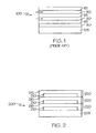
- Multilayer, thin film barrier composites having alternating layers of barrier material and polymer material are known. These composites are typically formed by depositing alternating layers of barrier material and polymer material, such as by vapor deposition. If the polymer layers are deposited over the entire surface of the substrate, then the edges of the polymer layers are exposed to oxygen, moisture, and other contaminants. This potentially allows the moisture, oxygen, or other contaminants to diffuse laterally into an encapsulated environmentally sensitive device from the edge of the composite, as shown in Fig. 1 .
- the multilayer, thin film barrier composite 100 includes a substrate 105 and alternating layers of decoupling material 110 and barrier material 115. The scale of Fig. 1 is greatly expanded in the vertical direction.
- the area of the substrate 105 will typically vary from a few square centimeters to several square meters.
- the barrier layers 115 are typically a few hundred Angstroms thick, while the decoupling layers 110 are generally less than ten microns thick.
- the lateral diffusion rate of moisture and oxygen is finite, and this will eventually compromise the encapsulation.
- One way to reduce the problem of edge diffusion is to provide long edge diffusion paths. However, this decreases the area of the substrate which is usable for active environmentally sensitive devices. In addition, it only lessens the problem, but does not eliminate it.
- a similar edge diffusion problem will arise when a substrate containing a multilayer, thin film barrier composite is scribed and separated to create individual components.
- U.S. Patent No. 6,150,187 relates to the encapsulation by sealing with multiple polymer films for extending the lifetime of a flexible organic or polymer light emitting device.
- US 2001/0015620 A1 and U.S. Patent No. 6,268,695 B1 disclose an environmental barrier for an OLED.
- the environmental barrier has a foundation and a cover. Both the foundation and cover have a first polymer layer, a ceramic layer, and a second polymer layer.
- EP 0 777 281 A2 discloses a method of passivating electroluminescent organic devices positioned on a supporting substrate including the steps of overcoating or capping the individual pixels with a layer of stable metal, overcoating the layer of stable metal with a buffer system including a buffer layer of organic material and a thermal coefficient matching layer on the buffer layer, depositing a low permeability inorganic layer over the coefficient matching layer, and sealing the electroluminescent organic device with an epoxy or polymer laminated foil.
- the present invention solves this need by providing an edge-sealed barrier film composite.
- the composite comprises a substrate, and at least one initial barrier stack adjacent to the substrate, the at least one initial barrier stack comprising at least one decoupling layer and at least two barrier layers, wherein a first decoupling layer of a first initial barrier stack has an area and wherein a first barrier layer of the first initial barrier stack has an area and wherein a second barrier layer of the first initial barrier stack has an area, the area of the first barrier layer being greater than the area of the first decoupling layer and the area of the second barrier layer being greater than the area of the first decoupling layer, and wherein the first barrier layer is in contact with the second barrier layer, sealing the first decoupling layer between the first barrier layer and the second barrier layer.
- the barrier layer is a barrier for oxygen, moisture, other contaminants, or combinations thereof, and the decoupling layer has improved surface planarity compared to a previous layer.
- adjacent we mean next to, but not necessarily directly next to. There can be additional layers intervening between the substrate and the barrier stacks.
- the first layer can be either a decoupling layer or a barrier layer, as can the last layer.
- One or more barrier stacks can include at least two decoupling layers and/or at least two barrier layers.
- the decoupling layers can be made from materials including, but not limited to, organic polymers, inorganic polymers, organometallic polymers, hybrid organic/inorganic polymer systems, silicates, and combinations thereof.
- the decoupling layers can be made of the same decoupling material or different decoupling materials.
- Suitable barrier materials include, but are not limited to, metals, metal oxides, metal nitrides, metal carbides, metal oxynitrides, metal oxyborides, and combinations thereof. Suitable barrier materials also include, but are not limited to, opaque metals, opaque ceramics, opaque polymers, and opaque cermets, and combinations thereof.
- the barrier layers can be made of the same barrier material or different barrier material.
- the composite can include an environmentally sensitive device.
- Environmentally sensitive devices include, but are not limited to, organic light emitting devices, liquid crystal displays, displays using electrophoretic inks, light emitting diodes, light emitting polymers, electroluminescent devices, phosphorescent devices, electrophoretic inks, organic solar cells, inorganic solar cells, thin film batteries, and thin film devices with vias, and combinations thereof.
- the edge-sealed, encapsulated environmentally sensitive device further comprises: at least one additional barrier stack adjacent to the environmentally sensitive device on a side opposite the at least one initial barrier stack, the at least one additional barrier stack comprising at least one decoupling layer and at least one barrier layer, wherein a first decoupling layer of a first additional barrier stack has an area and wherein a first barrier layer of the first additional barrier stack has an area, the area of the first barrier layer of the first additional barrier stack being greater than the area of the first decoupling layer of the first additional barrier stack, wherein the first decoupling layer of the first additional barrier stack is sealed by the first barrier layer of the first additional barrier stack within the area of the first barrier layer, and wherein the environmentally sensitive device is sealed between the at least one initial barrier stack and the at least one additional barrier stack.
- a second aspect of the invention is a method of making an edge-sealed barrier film composite.
- the method includes providing a substrate, and placing at least one initial barrier stack adjacent to the substrate, the at least one initial barrier stack comprising at least one decoupling layer and at least two barrier layers, wherein a first decoupling layer of a first initial barrier stack has an area and wherein a first barrier layer of the first initial barrier stack has an area and wherein a second barrier layer has an area, the area of the first barrier layer being greater than the area of the first decoupling layer, and the area of the second barrier layer being greater than the area of the first decoupling layer, and wherein the first barrier layer is in contact with the second barrier layer, sealing the first decoupling layer between the first barrier layer and the second barrier layer.
- the barrier layer is a barrier for oxygen, moisture, other contaminants, or combinations thereof, and the decoupling layer has improved surface planarity compared to a previous layer.
- Placing the at least one barrier stack adjacent to the substrate includes, but is not limited to, depositing the at least one barrier stack adjacent to the substrate, and laminating the at least one barrier stack adjacent to the substrate.
- the barrier layers can be deposited before or after the decoupling layers, depending on the particular application and structure.
- Depositing the at least one barrier stack may include, but is not limited to, providing a mask with at least one opening, depositing the first decoupling layer through the at least one opening in the mask, and depositing the first barrier layer.
- depositing the at least one barrier stack adjacent to the substrate may include, but is not limited to, depositing the first decoupling layer having an initial area of decoupling material which is greater than the area of the first decoupling layer, etching the first decoupling layer having the initial area of decoupling material to remove a portion of the decoupling material so that the first decoupling layer has the area of the first decoupling layer, and depositing the first barrier layer.
- Etching the first decoupling layer may include, but is not limited to, providing a solid mask over the first decoupling layer having the initial area of decoupling material, and etching the first decoupling layer having the initial area of decoupling material to remove the portion of the decoupling material outside the solid mask so that the first decoupling layer has the area of the first decoupling layer.
- the first decoupling layer may be etched so that at least one edge of the first decoupling layer has a gradual slope.
- a reactive plasma may be used to etch the decoupling layers. Reactive plasmas include, but are not limited to O 2 , CF 4 , H 2 , and combinations thereof.
- the method may include placing an environmentally sensitive device adjacent to the substrate before the at least one initial barrier stack is placed thereon. Alternatively, the method may include placing the environmentally sensitive device adjacent to the at least one initial barrier stack after the at least one initial barrier stack is placed on the substrate. The method may also include placing at least one additional barrier stack adjacent to the environmentally sensitive device on a side opposite the substrate, the at least one additional barrier stack comprising at least one decoupling layer and at least one barrier layer, wherein a first decoupling layer of a first additional barrier stack has an area and wherein a first barrier layer of the first additional barrier stack has an area, the area of the first barrier layer of the first additional barrier stack being greater than the area of the first decoupling layer of the first additional barrier stack, and wherein the first decoupling layer of the first additional barrier stack is sealed by the first barrier layer of the first additional barrier stack within the area of the first barrier layer.
- Laminating the at least one barrier stack adjacent to the substrate may be performed using a number of processes including, but not limited to, heat, solder, adhesive, ultrasonic welding, and pressure.
- the method may include depositing a ridge on the substrate before depositing the at least one barrier stack adjacent to the substrate, the ridge interfering with the deposition of the first decoupling layer so that the area of the first barrier layer is greater than the area of the first decoupling layer and the first decoupling layer is sealed by the first barrier layer within the area of the first barrier layer.
- Fig. 2 shows one embodiment of an edge-sealed, barrier composite 200.
- the composite 200 includes a substrate 205.
- the substrate can be any suitable substrate, and can be either rigid or flexible.
- Suitable substrates include, but are not limited to: polymers, for example, polyethylene terephthalate (PET), polyethylene naphthalate (PEN), or high temperature polymers, such as polyether sulfone (PES), polyimides, or Transphan TM (a high glass transition temperature cyclic olefin polymer available from Lofo High Tech Film, GMBH of Weil am Rhein, Germany); metals and metal foils; paper; fabric; glass, including thin, flexible, glass sheet (for example, flexible glass sheet available from Corning Inc. under the glass code 0211. This particular thin, flexible glass sheet has a thickness of less than 0.6 mm and will bend at a radium of about 8 inches.); ceramics; semiconductors; silicon; and combinations thereof.
- Fig. 2 shows three initial barrier stacks 220 adjacent to the substrate 205.
- the initial barrier stacks 220 include a decoupling layer 210 and a barrier layer 215.
- the barrier layer 215 has an area greater than the area of the decoupling layer 210. As a result, the barrier layer 215 extends beyond the edges of the decoupling layer 210, sealing the decoupling layer 210 within the area covered by the barrier layer 215. Because the decoupling layers 210 are sealed within the area covered by the barrier layers 215, ambient moisture, oxygen, and other contaminants cannot diffuse through the decoupling layers to the environmentally sensitive device.
- Fig. 2 shows three initial barrier stacks 220.
- the number of barrier stacks is not limited. The number of barrier stacks needed depends on the substrate material used and the level of permeation resistance needed for the particular application. One or two barrier stacks may provide sufficient barrier properties for some applications. The most stringent applications may require five or more barrier stacks.
- Each of the initial barrier stacks 220 shown in Fig. 2 has one barrier layer 215 and one decoupling layer 210.
- the barrier stacks can have one or more decoupling layers and one or more barrier layers. There could be one decoupling layer and one barrier layer, there could be one or more decoupling layers on one side of one or more barrier layers, there could be one or more decoupling layers on both sides of one or more barrier layers, or there could be one or more barrier layers on both sides of one or more decoupling layers.
- At least one of the barrier stacks has at least one decoupling layer and at least two barrier layers each having an area greater than the area of a first decoupling layer, and wherein the first decoupling layer is sealed between a first and a second barrier layer, as previously described.
- the barrier layers in the barrier stacks can be made of the same material or of a different material, as can the decoupling layers.
- the barrier layers are typically about 100-400 ⁇ thick, and the decoupling layers are typically about 1000-10,000 ⁇ thick.
- barrier stacks 220 are shown as having the same layers in the same order, this is not necessary.
- the barrier stacks can have the same or different layers, and the layers can be in the same or different sequences.
- a composite can be made with a single barrier stack having one decoupling layer and two barrier layers, there will typically be at least two barrier stacks, each of the second and further barrier stacks having one (or more) decoupling layer and one (or more) barrier layer.
- the first layer can be either a decoupling layer or a barrier layer, as can the last layer.
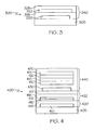
- Fig. 3 shows an edge-sealed, encapsulated environmentally sensitive device 300.
- a substrate 305 with an environmentally sensitive device 330 adjacent to it.
- a barrier stack 340 adjacent to the environmentally sensitive device 330.
- the barrier stack includes one decoupling layer 310 and two barrier layers 315, 325.
- the barrier layer 315 has an area greater than that of the environmentally sensitive device 330.
- the environmentally sensitive device 330 is sealed within the barrier layer 315.
- the barrier layers 315, 325 have an area greater than the area of the decoupling layer 310 so the decoupling layer 310 is sealed between the barrier layers 315, 325.
- the environmentally sensitive device can be any device requiring protection from moisture, gas, or other contaminants.
- Environmentally sensitive devices include, but are not limited to, organic light emitting devices, liquid crystal displays, displays using electrophoretic inks, light emitting diodes, light emitting polymers, electroluminescent devices, phosphorescent devices, electrophoretic inks, organic solar cells, inorganic solar cells, thin film batteries, and thin film devices with vias, and combinations thereof.
- the barrier layers It is not required that all of the barrier layers have an area greater than all of the decoupling layers, but at least one of the barrier layers must have an area greater than at least one of the decoupling layers. If not all of the barrier layers have an area greater than of the decoupling layers, the barrier layers which do have an area greater than the decoupling layers should form a seal around those which do not so that there are no exposed decoupling layers within the barrier composite, although, clearly it is a matter of degree. The fewer the edge areas of decoupling layers exposed, the less the edge diffusion. If some diffusion is acceptable, then a complete barrier is not required.
- Fig. 4 shows an edge-sealed, encapsulated environmentally sensitive device 400.
- a substrate 405 which can be removed after the device is made, if desired.
- the environmentally sensitive device 430 is encapsulated between two initial barrier stacks 420, 422 on one side and one additional barrier stack 440 on the other side.
- Barrier stack 420 has a barrier layer 415 which has an area greater than the area of the decoupling layer 410 which seals the decoupling layer 410 within the area of the barrier layer 415.
- Barrier stack 422 has two barrier layers 415, 417 and two decoupling layers 410, 412.
- Barrier layer 415 has an area greater than that of the decoupling layers 410, 412 which seals the decoupling layers 410, 412 within the area of the barrier layer 415.
- Barrier stack 440 includes two decoupling layers 410 and two barrier layers 415 which may be of approximately the same size. Barrier stack 440 also includes barrier layer 435 which has an area greater than the area of the decoupling layers 410 which seals the decoupling layers 410 within the area of barrier layer 435.
- the barrier layer which seals the decoupling layer may be the first barrier layer in the barrier stack, as shown in barrier stack 420. It may also be a second (or later) barrier layer as shown in barrier stack 440. Barrier layer 435 which seals the barrier stack 440 is the third barrier layer in the barrier stack following two barrier layers 415 which do not seal the barrier stack.
- first decoupling layer and first barrier layer in the claims does not refer to the actual sequence of layers, but to layers which meet the limitations.
- first initial barrier stack and first additional barrier stack do not refer to the actual sequence of the initial and additional barrier stacks.
- the barrier stack may include one or more decoupling layers.
- the decoupling layers may be made from the same decoupling material or different decoupling material.
- the decoupling layer can be made of any suitable decoupling material, including, but not limited to, organic polymers, inorganic polymers, organometallic polymers, hybrid organic/inorganic polymer systems, silicates, and combinations thereof.
- Organic polymers include, but are not limited to, urethanes, polyamides, polyimides, polybutylenes, isobutylene isoprene, polyolefins, epoxies, parylenes, benzocyclobutadiene, polynorbornenes, polyarylethers, polycarbonates, alkyds, polyaniline, ethylene vinyl acetate, ethylene acrylic acid, and combinations thereof.
- Inorganic polymers include, but are not limited to, silicones, polyphosphazenes, polysilazanes, polycarbosilanes, polycarboranes, carborane siloxanes, polysilanes, phosphonitriles, sulfur nitride polymers, siloxanes, and combinations thereof.
- Organometallic polymers include, but are not limited to, organometallic polymers of main group metals, transition metals, and lanthanide/actinide metals, or combinations thereof.
- Hybrid organic/inorganic polymer systems include, but are not limited to, organically modified silicates, preceramic polymers, polyimide-silica hybrids, (meth)acrylate-silica hybrids, polydimethylsiloxane-silica hybrid, ceramers, and combinations thereof.
- the barrier stack may include one or more barrier layers.
- the barrier layers may be made from the same barrier material or different barrier material.
- the barrier layer can be made from any suitable barrier material.
- the barrier material can be transparent or opaque depending on what the composite is to be used for.
- Suitable barrier materials include, but are not limited to, metals, metal oxides, metal nitrides, metal carbides, metal oxynitrides, metal oxyborides, and combinations thereof.
- Metals include, but are not limited to, aluminum, titanium, indium, tin, tantalum, zirconium, niobium, hafnium, yttrium, nickel, tungsten, chromium, zinc, alloys thereof, and combinations thereof.
- Metal oxides include, but are not limited to, silicon oxide, aluminum oxide, titanium oxide, indium oxide, tin oxide, indium tin oxide, tantalum oxide, zirconium oxide, niobium oxide, hafnium oxide, yttrium oxide, nickel oxide, tungsten oxide, chromium oxide, zinc oxide, and combinations thereof.
- Metal nitrides include, but are not limited to, aluminum nitride, silicon nitride, boron nitride, germanium nitride, chromium nitride, nickel nitride, and combinations thereof.
- Metal carbides include, but are not limited to, boron carbide, tungsten carbide, silicon carbide, and combinations thereof.
- Metal oxynitrides include, but are not limited to, aluminum oxynitride, silicon oxynitride, boron oxynitride, and combinations thereof.
- Metal oxyborides include, but are limited to, zirconium oxyboride, titanium oxyboride, and combinations thereof.
- Suitable barrier materials also include, but are not limited to, opaque metals, opaque ceramics, opaque polymers, and opaque cennets, and combinations thereof.
- Opaque cermets include, but are not limited to, zirconium nitride, titanium nitride, hafnium nitride, tantalum nitride, niobium nitride, tungsten disilicide, titanium diboride, and zirconium diboride, and combinations thereof.
- the barrier layers may be deposited by any suitable process including, but not limited to, conventional vacuum processes such as sputtering, evaporation, sublimation, chemical vapor deposition (CVD), plasma enhanced chemical vapor deposition (PECVD), electron cyclotron resonance-plasma enhanced vapor deposition (ECR-PECVD), and combinations thereof.
- CVD chemical vapor deposition
- PECVD plasma enhanced chemical vapor deposition
- ECR-PECVD electron cyclotron resonance-plasma enhanced vapor deposition
- the decoupling layer can be produced by a number of known processes which provide improved surface planarity, including both atmospheric processes and vacuum processes.
- the decoupling layer may be formed by depositing a layer of liquid and subsequently processing the layer of liquid into a solid film. Depositing the decoupling layer as a liquid allows the liquid to flow over the defects in the substrate or previous layer, filling in low areas, and covering up high points, providing a surface with significantly improved planarity. When the decoupling layer is processed into a solid film, the improved surface planarity is retained.
- Suitable processes for depositing a layer of liquid material and processing it into a solid film include, but are not limited to, vacuum processes such as those described in United States Patent Nos.
- One way to make a decoupling layer involves depositing a polymer precursor, such as a (meth)acrylate containing polymer precursor, and then polymerizing it in situ to form the decoupling layer.
- a polymer precursor means a material which can be polymerized to form a polymer, including, but not limited to, monomers, oligomers, and resins.
- a preceramic precursor could be deposited as a liquid by spin coating and then converted to a solid layer. Full thermal conversion is possible for a film of this type directly on a glass or oxide coated substrate.
- Electron beam techniques could be used to crosslink and/or densify some of these types of polymers and can be combined with thermal techniques to overcome some of the substrate thermal limitations, provided the substrate can handle the electron beam exposure.
- a decoupling layer involves depositing a material, such as a polymer precursor, as a liquid at a temperature above its melting point and subsequently freezing it in place.
- One method of making the composite of the present invention includes providing a substrate, and depositing a barrier layer adjacent to the substrate at a barrier deposition station.
- the substrate with the barrier layer is moved to a decoupling material deposition station.
- a mask is provided with an opening which limits the deposition of the decoupling layer to an area which is smaller than, and contained within, the area covered by the barrier layer.
- the first layer deposited could be either the barrier layer or the decoupling layer, depending on the design of the composite.
- the decoupling material may be deposited through multiple openings in a single shadow mask, or through multiple shadow masks. This allows the motherglass to be subsequently diced into individual environmentally sensitive devices, each of which is edge sealed.
- the mask may be in the form of a rectangle with the center removed (like a picture frame).
- the decoupling material is then deposited through the opening in the mask.
- the layer of decoupling material formed in this way will cover an area less than the area covered by the layer of barrier material.
- This type of mask can be used in either a batch process or a roll coating process operated in a step and repeat mode. With these processes, all four edges of the decoupling layer will be sealed by the barrier material when a second barrier layer which has an area greater than the area of the decoupling layer is deposited over the decoupling layer.
- the method can also be used in a continuous roll to roll process using a mask having two sides which extend inward over the substrate.
- the opening is formed between the two sides of the mask which allows continuous deposition of decoupling material.
- the mask may have transverse connections between the two sides so long as they are not in the deposition area for the decoupling layer.
- the mask is positioned laterally and at a distance from the substrate so as to cause the decoupling material to be deposited over an area less than that of the barrier layer. In this arrangement, the lateral edges of the decoupling layer are sealed by the barrier layer.
- the substrate can then be moved to a barrier deposition station (either the original barrier deposition station or a second one), and a second layer of barrier material deposited on the decoupling layer. Since the area covered by the first barrier layer is greater than the area of the decoupling layer, the decoupling layer is sealed between the two barrier layers. These deposition steps can be repeated if necessary until sufficient barrier material is deposited for the particular application.
- a barrier deposition station either the original barrier deposition station or a second one
- the substrate can be passed by one or more decoupling material deposition stations one or more times before being moved to the barrier deposition station.
- the decoupling layers can be made from the same decoupling material or different decoupling material.
- the decoupling layers can be deposited using the same process or using different processes.
- one or more barrier stacks can include two or more barrier layers.
- the barrier layers can be formed by passing the substrate (either before or after the decoupling layers have been deposited) past one or more barrier deposition stations one or more times, building up the number of layers desired.
- the layers can be made of the same or different barrier material, and they can be deposited using the same or different processes.
- the method involves providing a substrate and depositing a layer of barrier material on the surface of the substrate at a barrier deposition station.
- the substrate with the barrier layer is moved to a decoupling material deposition station where a layer of decoupling material is deposited over substantially the whole surface of the barrier layer.
- a solid mask is then placed over the substrate with the barrier layer and the decoupling layer. The mask protects the central area of the surface, which would include the areas covered by the active environmentally sensitive devices.
- a reactive plasma can be used to etch away the edges of the layer of decoupling material outside the mask, which results in the layer of etched decoupling material covering an area less than the area covered by the layer of barrier material.
- Suitable reactive plasmas include, but are not limited to, O 2 , CF 4 , and H 2 , and combinations thereof.
- a layer of barrier material covering an area greater than that covered by the etched decoupling layer can then be deposited, scaling the etched decoupling layer between the layers of barrier material.
- the deposition and etching steps can be repeated until sufficient barrier material is deposited.
- This method can be used in a batch process or in a roll coating process operated in a step and repeat mode. In these processes, all four edges of the decoupling layer may be etched.
- This method can also be used in continuous roll to roll processes. In this case, only the edges of the decoupling material in the direction of the process are etched.
- the cut edges will expose the edges of the decoupling layers. These cut edges may require additional sealing if the exposure compromises barrier performance.
- One method for sealing edges which are to be cut involves depositing a ridge on the substrate before depositing the barrier stack.
- the ridge interferes with the deposition of the decoupling layer so that the area of barrier material is greater than the area of decoupling material and the decoupling layer is sealed by the barrier layer within the area of barrier material.
- the ridge should be fairly pointed, for example, triangular shaped, in order to interrupt the deposition and allow the layers of barrier material to extend beyond the layers of decoupling material.
- the ridge can be deposited anywhere that a cut will need to be made, such as around individual environmentally sensitive devices.
- the ridge can be made of any suitable material, including, but not limited to, photoresist and barrier materials, such as described previously.
Landscapes
- Chemical & Material Sciences (AREA)
- Chemical Kinetics & Catalysis (AREA)
- Electrochemistry (AREA)
- General Chemical & Material Sciences (AREA)
- Inorganic Chemistry (AREA)
- Physics & Mathematics (AREA)
- Optics & Photonics (AREA)
- Electroluminescent Light Sources (AREA)
- Laminated Bodies (AREA)
- Encapsulation Of And Coatings For Semiconductor Or Solid State Devices (AREA)
- Application Of Or Painting With Fluid Materials (AREA)
Abstract
Description
- The invention relates generally to multilayer, thin film barrier composites, and more particularly, to multilayer, thin film barrier composites having the edges sealed against lateral moisture and gas diffusion.
- Multilayer, thin film barrier composites having alternating layers of barrier material and polymer material are known. These composites are typically formed by depositing alternating layers of barrier material and polymer material, such as by vapor deposition. If the polymer layers are deposited over the entire surface of the substrate, then the edges of the polymer layers are exposed to oxygen, moisture, and other contaminants. This potentially allows the moisture, oxygen, or other contaminants to diffuse laterally into an encapsulated environmentally sensitive device from the edge of the composite, as shown in
Fig. 1 . The multilayer, thin film barrier composite 100 includes asubstrate 105 and alternating layers of decouplingmaterial 110 andbarrier material 115. The scale ofFig. 1 is greatly expanded in the vertical direction. The area of thesubstrate 105 will typically vary from a few square centimeters to several square meters. Thebarrier layers 115 are typically a few hundred Angstroms thick, while the decouplinglayers 110 are generally less than ten microns thick. The lateral diffusion rate of moisture and oxygen is finite, and this will eventually compromise the encapsulation. One way to reduce the problem of edge diffusion is to provide long edge diffusion paths. However, this decreases the area of the substrate which is usable for active environmentally sensitive devices. In addition, it only lessens the problem, but does not eliminate it. - A similar edge diffusion problem will arise when a substrate containing a multilayer, thin film barrier composite is scribed and separated to create individual components.
-
U.S. Patent No. 6,150,187 relates to the encapsulation by sealing with multiple polymer films for extending the lifetime of a flexible organic or polymer light emitting device. - High Resolution Color Organic Light Emitting Diode Microdisplay Fabrication Method, Graupner et al. SPIE Proceedings (2000), reports experimental results on the evaluation of a sealing technique for organic light emitting diodes. A conformal polymer/metal (oxide)/polymer coating was used.
-
US 2001/0015620 A1 andU.S. Patent No. 6,268,695 B1 disclose an environmental barrier for an OLED. The environmental barrier has a foundation and a cover. Both the foundation and cover have a first polymer layer, a ceramic layer, and a second polymer layer. -
EP 0 777 281 A2 discloses a method of passivating electroluminescent organic devices positioned on a supporting substrate including the steps of overcoating or capping the individual pixels with a layer of stable metal, overcoating the layer of stable metal with a buffer system including a buffer layer of organic material and a thermal coefficient matching layer on the buffer layer, depositing a low permeability inorganic layer over the coefficient matching layer, and sealing the electroluminescent organic device with an epoxy or polymer laminated foil. - Thus, there is a need for an edge-sealed barrier film composite, and for a method of making such a composite.
- The present invention solves this need by providing an edge-sealed barrier film composite. The composite comprises a substrate, and at least one initial barrier stack adjacent to the substrate, the at least one initial barrier stack comprising at least one decoupling layer and at least two barrier layers, wherein a first decoupling layer of a first initial barrier stack has an area and wherein a first barrier layer of the first initial barrier stack has an area and wherein a second barrier layer of the first initial barrier stack has an area, the area of the first barrier layer being greater than the area of the first decoupling layer and the area of the second barrier layer being greater than the area of the first decoupling layer, and wherein the first barrier layer is in contact with the second barrier layer, sealing the first decoupling layer between the first barrier layer and the second barrier layer. The barrier layer is a barrier for oxygen, moisture, other contaminants, or combinations thereof, and the decoupling layer has improved surface planarity compared to a previous layer. By adjacent, we mean next to, but not necessarily directly next to. There can be additional layers intervening between the substrate and the barrier stacks.
- The first layer can be either a decoupling layer or a barrier layer, as can the last layer. One or more barrier stacks can include at least two decoupling layers and/or at least two barrier layers.
- The decoupling layers can be made from materials including, but not limited to, organic polymers, inorganic polymers, organometallic polymers, hybrid organic/inorganic polymer systems, silicates, and combinations thereof. The decoupling layers can be made of the same decoupling material or different decoupling materials.
- Suitable barrier materials include, but are not limited to, metals, metal oxides, metal nitrides, metal carbides, metal oxynitrides, metal oxyborides, and combinations thereof. Suitable barrier materials also include, but are not limited to, opaque metals, opaque ceramics, opaque polymers, and opaque cermets, and combinations thereof. The barrier layers can be made of the same barrier material or different barrier material.
- The composite can include an environmentally sensitive device. Environmentally sensitive devices include, but are not limited to, organic light emitting devices, liquid crystal displays, displays using electrophoretic inks, light emitting diodes, light emitting polymers, electroluminescent devices, phosphorescent devices, electrophoretic inks, organic solar cells, inorganic solar cells, thin film batteries, and thin film devices with vias, and combinations thereof.
- In another embodiment of the invention the edge-sealed, encapsulated environmentally sensitive device further comprises: at least one additional barrier stack adjacent to the environmentally sensitive device on a side opposite the at least one initial barrier stack, the at least one additional barrier stack comprising at least one decoupling layer and at least one barrier layer, wherein a first decoupling layer of a first additional barrier stack has an area and wherein a first barrier layer of the first additional barrier stack has an area, the area of the first barrier layer of the first additional barrier stack being greater than the area of the first decoupling layer of the first additional barrier stack, wherein the first decoupling layer of the first additional barrier stack is sealed by the first barrier layer of the first additional barrier stack within the area of the first barrier layer, and wherein the environmentally sensitive device is sealed between the at least one initial barrier stack and the at least one additional barrier stack.
- A second aspect of the invention is a method of making an edge-sealed barrier film composite. The method includes providing a substrate, and placing at least one initial barrier stack adjacent to the substrate, the at least one initial barrier stack comprising at least one decoupling layer and at least two barrier layers, wherein a first decoupling layer of a first initial barrier stack has an area and wherein a first barrier layer of the first initial barrier stack has an area and wherein a second barrier layer has an area, the area of the first barrier layer being greater than the area of the first decoupling layer, and the area of the second barrier layer being greater than the area of the first decoupling layer, and wherein the first barrier layer is in contact with the second barrier layer, sealing the first decoupling layer between the first barrier layer and the second barrier layer. The barrier layer is a barrier for oxygen, moisture, other contaminants, or combinations thereof, and the decoupling layer has improved surface planarity compared to a previous layer.
- Placing the at least one barrier stack adjacent to the substrate includes, but is not limited to, depositing the at least one barrier stack adjacent to the substrate, and laminating the at least one barrier stack adjacent to the substrate.
- The barrier layers can be deposited before or after the decoupling layers, depending on the particular application and structure.
- Depositing the at least one barrier stack may include, but is not limited to, providing a mask with at least one opening, depositing the first decoupling layer through the at least one opening in the mask, and depositing the first barrier layer.
- Alternatively, depositing the at least one barrier stack adjacent to the substrate may include, but is not limited to, depositing the first decoupling layer having an initial area of decoupling material which is greater than the area of the first decoupling layer, etching the first decoupling layer having the initial area of decoupling material to remove a portion of the decoupling material so that the first decoupling layer has the area of the first decoupling layer, and depositing the first barrier layer. Etching the first decoupling layer may include, but is not limited to, providing a solid mask over the first decoupling layer having the initial area of decoupling material, and etching the first decoupling layer having the initial area of decoupling material to remove the portion of the decoupling material outside the solid mask so that the first decoupling layer has the area of the first decoupling layer. The first decoupling layer may be etched so that at least one edge of the first decoupling layer has a gradual slope. A reactive plasma may be used to etch the decoupling layers. Reactive plasmas include, but are not limited to O2, CF4, H2, and combinations thereof.
- The method may include placing an environmentally sensitive device adjacent to the substrate before the at least one initial barrier stack is placed thereon. Alternatively, the method may include placing the environmentally sensitive device adjacent to the at least one initial barrier stack after the at least one initial barrier stack is placed on the substrate. The method may also include placing at least one additional barrier stack adjacent to the environmentally sensitive device on a side opposite the substrate, the at least one additional barrier stack comprising at least one decoupling layer and at least one barrier layer, wherein a first decoupling layer of a first additional barrier stack has an area and wherein a first barrier layer of the first additional barrier stack has an area, the area of the first barrier layer of the first additional barrier stack being greater than the area of the first decoupling layer of the first additional barrier stack, and wherein the first decoupling layer of the first additional barrier stack is sealed by the first barrier layer of the first additional barrier stack within the area of the first barrier layer.
- Laminating the at least one barrier stack adjacent to the substrate may be performed using a number of processes including, but not limited to, heat, solder, adhesive, ultrasonic welding, and pressure.
- The method may include depositing a ridge on the substrate before depositing the at least one barrier stack adjacent to the substrate, the ridge interfering with the deposition of the first decoupling layer so that the area of the first barrier layer is greater than the area of the first decoupling layer and the first decoupling layer is sealed by the first barrier layer within the area of the first barrier layer.
-
Fig. 1 is a cross-section of a barrier composite of the prior art. -
Fig. 2 is a cross-section of one embodiment of an edge-sealed, barrier composite of the present invention. -
Fig. 3 is a cross-section of an embodiment of an edge-sealed, encapsulated environmentally sensitive device of the present invention. -
Fig. 4 is a cross-section of another embodiment of an edge-sealed, encapsulated environmentally sensitive device of the present invention. -
Fig. 2 shows one embodiment of an edge-sealed, barrier composite 200. The composite 200 includes asubstrate 205. The substrate can be any suitable substrate, and can be either rigid or flexible. Suitable substrates include, but are not limited to: polymers, for example, polyethylene terephthalate (PET), polyethylene naphthalate (PEN), or high temperature polymers, such as polyether sulfone (PES), polyimides, or Transphan™ (a high glass transition temperature cyclic olefin polymer available from Lofo High Tech Film, GMBH of Weil am Rhein, Germany); metals and metal foils; paper; fabric; glass, including thin, flexible, glass sheet (for example, flexible glass sheet available from Corning Inc. under the glass code 0211. This particular thin, flexible glass sheet has a thickness of less than 0.6 mm and will bend at a radium of about 8 inches.); ceramics; semiconductors; silicon; and combinations thereof. -
Fig. 2 shows three initial barrier stacks 220 adjacent to thesubstrate 205. Theinitial barrier stacks 220 include adecoupling layer 210 and abarrier layer 215. Thebarrier layer 215 has an area greater than the area of thedecoupling layer 210. As a result, thebarrier layer 215 extends beyond the edges of thedecoupling layer 210, sealing thedecoupling layer 210 within the area covered by thebarrier layer 215. Because the decoupling layers 210 are sealed within the area covered by the barrier layers 215, ambient moisture, oxygen, and other contaminants cannot diffuse through the decoupling layers to the environmentally sensitive device. -
Fig. 2 shows three initial barrier stacks 220. However, the number of barrier stacks is not limited. The number of barrier stacks needed depends on the substrate material used and the level of permeation resistance needed for the particular application. One or two barrier stacks may provide sufficient barrier properties for some applications. The most stringent applications may require five or more barrier stacks. - Each of the initial barrier stacks 220 shown in
Fig. 2 has onebarrier layer 215 and onedecoupling layer 210. However, the barrier stacks can have one or more decoupling layers and one or more barrier layers. There could be one decoupling layer and one barrier layer, there could be one or more decoupling layers on one side of one or more barrier layers, there could be one or more decoupling layers on both sides of one or more barrier layers, or there could be one or more barrier layers on both sides of one or more decoupling layers. The important feature is that at least one of the barrier stacks has at least one decoupling layer and at least two barrier layers each having an area greater than the area of a first decoupling layer, and wherein the first decoupling layer is sealed between a first and a second barrier layer, as previously described. The barrier layers in the barrier stacks can be made of the same material or of a different material, as can the decoupling layers. The barrier layers are typically about 100-400 Å thick, and the decoupling layers are typically about 1000-10,000 Å thick. - Although the three initial barrier stacks 220 are shown as having the same layers in the same order, this is not necessary. The barrier stacks can have the same or different layers, and the layers can be in the same or different sequences.
- Although a composite can be made with a single barrier stack having one decoupling layer and two barrier layers, there will typically be at least two barrier stacks, each of the second and further barrier stacks having one (or more) decoupling layer and one (or more) barrier layer. In this case, of the second and further barrier stacks the first layer can be either a decoupling layer or a barrier layer, as can the last layer.
-
Fig. 3 shows an edge-sealed, encapsulated environmentally sensitive device 300. There is asubstrate 305 with an environmentallysensitive device 330 adjacent to it. There is abarrier stack 340 adjacent to the environmentallysensitive device 330. The barrier stack includes onedecoupling layer 310 and twobarrier layers barrier layer 315 has an area greater than that of the environmentallysensitive device 330. Thus, the environmentallysensitive device 330 is sealed within thebarrier layer 315. The barrier layers 315, 325 have an area greater than the area of thedecoupling layer 310 so thedecoupling layer 310 is sealed between the barrier layers 315, 325. - The environmentally sensitive device can be any device requiring protection from moisture, gas, or other contaminants. Environmentally sensitive devices include, but are not limited to, organic light emitting devices, liquid crystal displays, displays using electrophoretic inks, light emitting diodes, light emitting polymers, electroluminescent devices, phosphorescent devices, electrophoretic inks, organic solar cells, inorganic solar cells, thin film batteries, and thin film devices with vias, and combinations thereof.
- It is not required that all of the barrier layers have an area greater than all of the decoupling layers, but at least one of the barrier layers must have an area greater than at least one of the decoupling layers. If not all of the barrier layers have an area greater than of the decoupling layers, the barrier layers which do have an area greater than the decoupling layers should form a seal around those which do not so that there are no exposed decoupling layers within the barrier composite, although, clearly it is a matter of degree. The fewer the edge areas of decoupling layers exposed, the less the edge diffusion. If some diffusion is acceptable, then a complete barrier is not required.
-
Fig. 4 shows an edge-sealed, encapsulated environmentally sensitive device 400. There is asubstrate 405 which can be removed after the device is made, if desired. The environmentallysensitive device 430 is encapsulated between two initial barrier stacks 420, 422 on one side and oneadditional barrier stack 440 on the other side. -
Barrier stack 420 has abarrier layer 415 which has an area greater than the area of thedecoupling layer 410 which seals thedecoupling layer 410 within the area of thebarrier layer 415.Barrier stack 422 has twobarrier layers decoupling layers Barrier layer 415 has an area greater than that of the decoupling layers 410, 412 which seals the decoupling layers 410, 412 within the area of thebarrier layer 415. There is asecond barrier layer 417. - On the other side of the environmentally
sensitive device 430, there is anadditional barrier stack 440.Barrier stack 440 includes twodecoupling layers 410 and twobarrier layers 415 which may be of approximately the same size.Barrier stack 440 also includesbarrier layer 435 which has an area greater than the area of the decoupling layers 410 which seals the decoupling layers 410 within the area ofbarrier layer 435. - The barrier layer which seals the decoupling layer may be the first barrier layer in the barrier stack, as shown in
barrier stack 420. It may also be a second (or later) barrier layer as shown inbarrier stack 440.Barrier layer 435 which seals thebarrier stack 440 is the third barrier layer in the barrier stack following twobarrier layers 415 which do not seal the barrier stack. Thus, the use of the terms first decoupling layer and first barrier layer in the claims does not refer to the actual sequence of layers, but to layers which meet the limitations. Similarly, the terms first initial barrier stack and first additional barrier stack do not refer to the actual sequence of the initial and additional barrier stacks. - The barrier stack may include one or more decoupling layers. The decoupling layers may be made from the same decoupling material or different decoupling material. The decoupling layer can be made of any suitable decoupling material, including, but not limited to, organic polymers, inorganic polymers, organometallic polymers, hybrid organic/inorganic polymer systems, silicates, and combinations thereof. Organic polymers include, but are not limited to, urethanes, polyamides, polyimides, polybutylenes, isobutylene isoprene, polyolefins, epoxies, parylenes, benzocyclobutadiene, polynorbornenes, polyarylethers, polycarbonates, alkyds, polyaniline, ethylene vinyl acetate, ethylene acrylic acid, and combinations thereof. Inorganic polymers include, but are not limited to, silicones, polyphosphazenes, polysilazanes, polycarbosilanes, polycarboranes, carborane siloxanes, polysilanes, phosphonitriles, sulfur nitride polymers, siloxanes, and combinations thereof. Organometallic polymers include, but are not limited to, organometallic polymers of main group metals, transition metals, and lanthanide/actinide metals, or combinations thereof. Hybrid organic/inorganic polymer systems include, but are not limited to, organically modified silicates, preceramic polymers, polyimide-silica hybrids, (meth)acrylate-silica hybrids, polydimethylsiloxane-silica hybrid, ceramers, and combinations thereof.
- The barrier stack may include one or more barrier layers. The barrier layers may be made from the same barrier material or different barrier material. The barrier layer can be made from any suitable barrier material. The barrier material can be transparent or opaque depending on what the composite is to be used for. Suitable barrier materials include, but are not limited to, metals, metal oxides, metal nitrides, metal carbides, metal oxynitrides, metal oxyborides, and combinations thereof. Metals include, but are not limited to, aluminum, titanium, indium, tin, tantalum, zirconium, niobium, hafnium, yttrium, nickel, tungsten, chromium, zinc, alloys thereof, and combinations thereof. Metal oxides include, but are not limited to, silicon oxide, aluminum oxide, titanium oxide, indium oxide, tin oxide, indium tin oxide, tantalum oxide, zirconium oxide, niobium oxide, hafnium oxide, yttrium oxide, nickel oxide, tungsten oxide, chromium oxide, zinc oxide, and combinations thereof. Metal nitrides include, but are not limited to, aluminum nitride, silicon nitride, boron nitride, germanium nitride, chromium nitride, nickel nitride, and combinations thereof. Metal carbides include, but are not limited to, boron carbide, tungsten carbide, silicon carbide, and combinations thereof. Metal oxynitrides include, but are not limited to, aluminum oxynitride, silicon oxynitride, boron oxynitride, and combinations thereof. Metal oxyborides include, but are limited to, zirconium oxyboride, titanium oxyboride, and combinations thereof. Suitable barrier materials also include, but are not limited to, opaque metals, opaque ceramics, opaque polymers, and opaque cennets, and combinations thereof. Opaque cermets include, but are not limited to, zirconium nitride, titanium nitride, hafnium nitride, tantalum nitride, niobium nitride, tungsten disilicide, titanium diboride, and zirconium diboride, and combinations thereof.
- The barrier layers may be deposited by any suitable process including, but not limited to, conventional vacuum processes such as sputtering, evaporation, sublimation, chemical vapor deposition (CVD), plasma enhanced chemical vapor deposition (PECVD), electron cyclotron resonance-plasma enhanced vapor deposition (ECR-PECVD), and combinations thereof.
- The decoupling layer can be produced by a number of known processes which provide improved surface planarity, including both atmospheric processes and vacuum processes. The decoupling layer may be formed by depositing a layer of liquid and subsequently processing the layer of liquid into a solid film. Depositing the decoupling layer as a liquid allows the liquid to flow over the defects in the substrate or previous layer, filling in low areas, and covering up high points, providing a surface with significantly improved planarity. When the decoupling layer is processed into a solid film, the improved surface planarity is retained. Suitable processes for depositing a layer of liquid material and processing it into a solid film include, but are not limited to, vacuum processes such as those described in United States Patent Nos.
5,260,095 ,5,395,644 ,5,547,508 ,5,691,615 ,5,902,641 ,5,440,446 , and5,725,909 , which are incorporated herein by reference, and atmospheric processes such as spin coating and/or spraying. - One way to make a decoupling layer involves depositing a polymer precursor, such as a (meth)acrylate containing polymer precursor, and then polymerizing it in situ to form the decoupling layer. As used herein, the term polymer precursor means a material which can be polymerized to form a polymer, including, but not limited to, monomers, oligomers, and resins. As another example of a method of making a decoupling layer, a preceramic precursor could be deposited as a liquid by spin coating and then converted to a solid layer. Full thermal conversion is possible for a film of this type directly on a glass or oxide coated substrate. Although it cannot be fully converted to a ceramic at temperatures compatible with some flexible substrates, partial conversion to a cross-lined network structure would be satisfactory. Electron beam techniques could be used to crosslink and/or densify some of these types of polymers and can be combined with thermal techniques to overcome some of the substrate thermal limitations, provided the substrate can handle the electron beam exposure. Another example of making a decoupling layer involves depositing a material, such as a polymer precursor, as a liquid at a temperature above its melting point and subsequently freezing it in place.
- One method of making the composite of the present invention includes providing a substrate, and depositing a barrier layer adjacent to the substrate at a barrier deposition station. The substrate with the barrier layer is moved to a decoupling material deposition station. A mask is provided with an opening which limits the deposition of the decoupling layer to an area which is smaller than, and contained within, the area covered by the barrier layer. The first layer deposited could be either the barrier layer or the decoupling layer, depending on the design of the composite.
- In order to encapsulate multiple small environmentally sensitive devices contained on a single large motherglass, the decoupling material may be deposited through multiple openings in a single shadow mask, or through multiple shadow masks. This allows the motherglass to be subsequently diced into individual environmentally sensitive devices, each of which is edge sealed.
- For example, the mask may be in the form of a rectangle with the center removed (like a picture frame). The decoupling material is then deposited through the opening in the mask. The layer of decoupling material formed in this way will cover an area less than the area covered by the layer of barrier material. This type of mask can be used in either a batch process or a roll coating process operated in a step and repeat mode. With these processes, all four edges of the decoupling layer will be sealed by the barrier material when a second barrier layer which has an area greater than the area of the decoupling layer is deposited over the decoupling layer.
- The method can also be used in a continuous roll to roll process using a mask having two sides which extend inward over the substrate. The opening is formed between the two sides of the mask which allows continuous deposition of decoupling material. The mask may have transverse connections between the two sides so long as they are not in the deposition area for the decoupling layer. The mask is positioned laterally and at a distance from the substrate so as to cause the decoupling material to be deposited over an area less than that of the barrier layer. In this arrangement, the lateral edges of the decoupling layer are sealed by the barrier layer.
- The substrate can then be moved to a barrier deposition station (either the original barrier deposition station or a second one), and a second layer of barrier material deposited on the decoupling layer. Since the area covered by the first barrier layer is greater than the area of the decoupling layer, the decoupling layer is sealed between the two barrier layers. These deposition steps can be repeated if necessary until sufficient barrier material is deposited for the particular application.
- When one of the barrier stacks includes two or more decoupling layers, the substrate can be passed by one or more decoupling material deposition stations one or more times before being moved to the barrier deposition station. The decoupling layers can be made from the same decoupling material or different decoupling material. The decoupling layers can be deposited using the same process or using different processes.
- Similarly, one or more barrier stacks can include two or more barrier layers. The barrier layers can be formed by passing the substrate (either before or after the decoupling layers have been deposited) past one or more barrier deposition stations one or more times, building up the number of layers desired. The layers can be made of the same or different barrier material, and they can be deposited using the same or different processes.
- In another embodiment, the method involves providing a substrate and depositing a layer of barrier material on the surface of the substrate at a barrier deposition station. The substrate with the barrier layer is moved to a decoupling material deposition station where a layer of decoupling material is deposited over substantially the whole surface of the barrier layer. A solid mask is then placed over the substrate with the barrier layer and the decoupling layer. The mask protects the central area of the surface, which would include the areas covered by the active environmentally sensitive devices. A reactive plasma can be used to etch away the edges of the layer of decoupling material outside the mask, which results in the layer of etched decoupling material covering an area less than the area covered by the layer of barrier material. Suitable reactive plasmas include, but are not limited to, O2, CF4, and H2, and combinations thereof. A layer of barrier material covering an area greater than that covered by the etched decoupling layer can then be deposited, scaling the etched decoupling layer between the layers of barrier material.
- To ensure good coverage of the edge of the decoupling layer by the barrier layer, techniques for masking and etching the decoupling layer to produce a feathered edge, i.e., a gradual slope instead of a sharp step, may be employed. Several such techniques are known to those in the art, including, but not limited to, standing off the mask a short distance above a polymer surface to be etched.
- The deposition and etching steps can be repeated until sufficient barrier material is deposited. This method can be used in a batch process or in a roll coating process operated in a step and repeat mode. In these processes, all four edges of the decoupling layer may be etched. This method can also be used in continuous roll to roll processes. In this case, only the edges of the decoupling material in the direction of the process are etched.
- If a composite is made using a continuous process and the edged sealed composite is cut in the transverse direction, the cut edges will expose the edges of the decoupling layers. These cut edges may require additional sealing if the exposure compromises barrier performance.
- One method for sealing edges which are to be cut involves depositing a ridge on the substrate before depositing the barrier stack. The ridge interferes with the deposition of the decoupling layer so that the area of barrier material is greater than the area of decoupling material and the decoupling layer is sealed by the barrier layer within the area of barrier material. The ridge should be fairly pointed, for example, triangular shaped, in order to interrupt the deposition and allow the layers of barrier material to extend beyond the layers of decoupling material. The ridge can be deposited anywhere that a cut will need to be made, such as around individual environmentally sensitive devices. The ridge can be made of any suitable material, including, but not limited to, photoresist and barrier materials, such as described previously.
- While certain representative embodiments and details have been shown for purposes of illustrating the invention, it will be apparent to those skilled in the art that various changes in the compositions and methods disclosed herein may be made without departing from the scope of the invention, which is defined in the appended claims.
Claims (31)
- An edge-sealed barrier film composite comprising:a substrate; andat least one initial barrier stack adjacent to the substrate, the at least one initial barrier stack comprising at least one decoupling layer and at least two barrier layers, wherein a first decoupling layer of a first initial barrier stack has an area and wherein a first barrier layer of the first initial barrier stack has an area and wherein a second barrier layer of the first initial barrier stack has an area, the area of the first barrier layer being greater than the area of the first decoupling layer and the area of the second barrier layer being greater than the area of the first decoupling layer, and wherein the first barrier layer is in contact with the second barrier layer, sealing the first decoupling layer between the first barrier layer and the second barrier layer, wherein the barrier layer is a barrier for oxygen, moisture, other contaminants, or combinations thereof, and wherein the decoupling layer has improved surface planarity compared to a previous layer.
- The edge-sealed barrier film composite of claim 1 wherein the edge-sealed barrier film composite includes at least two initial barrier stacks, wherein a second initial barrier stack comprises one or more decoupling layers and one or more barrier layers.
- The edge-sealed barrier film composite of claim 1 wherein the edge-sealed barrier film composite includes at least two initial barrier stacks, wherein a first barrier layer of a second initial barrier stack has an area greater than an area of a first decoupling layer of the second initial barrier stack and wherein a barrier layer of the first initial barrier stack and the first barrier layer of the second initial barrier stack are in contact and seal the first decoupling layer of the second initial barrier stack between them.
- The edge-sealed barrier film composite of claim 1 wherein at least one initial barrier stack includes at least two decoupling layers.
- The edge-sealed barrier film composite of claim 1 further comprising an environmentally sensitive device, wherein the environmentally sensitive device is sensitive to oxygen, moisture, other contaminants, or combinations thereof.
- The edge-sealed barrier film composite of claim 5 wherein the environmentally sensitive device is selected from organic light emitting devices, liquid crystal displays, displays using electrophoretic inks, light emitting diodes, light emitting polymers, electroluminescent devices, phosphorescent devices, electrophoretic inks, organic solar cells, inorganic solar cells, thin film batteries, or thin film devices with vias, or combinations thereof.
- The edge-sealed barrier film composite of claim 5 wherein the environmentally sensitive device is adjacent to the substrate and located between the substrate and the at least one initial barrier stack, wherein at least one of the barrier layers of the at least one initial barrier stack has an area which is greater than an area of the environmentally sensitive device and wherein the at least one barrier layer of the at least one initial barrier stack is in contact with the substrate sealing the environmentally sensitive device between the at least one barrier layer of the at least one initial barrier stack and the substrate.
- The edge-sealed barrier film composite of claim 5 wherein the environmentally sensitive device is adjacent to the at least one initial barrier stack on a side opposite the substrate.
- The edge-sealed barrier film composite of claims 5-8 wherein the edge-sealed, encapsulated environmentally sensitive device includes at least two initial barrier stacks, wherein a first barrier layer of a second initial barrier stack has an area greater than an area of the first decoupling layer of the second initial barrier stack and wherein a barrier layer of the first initial barrier stack and the first barrier layer of the second initial barrier stack are in contact and seal the first decoupling layer of the second initial barrier stack between them.
- The edge-sealed barrier film composite of claims 1-9 wherein at least one of the decoupling layers is selected from organic polymers, inorganic polymers, organometallic polymers, hybrid organic/inorganic polymer systems, silicates, or combinations thereof.
- The edge-sealed barrier film composite of claims 1-10 wherein at least one of the barrier layers comprises a barrier material selected from metals, metal oxides, metal nitrides, metal carbides, metal oxynitrides, metal oxyborides, or combinations thereof.
- The edge-sealed barrier film composite of claims 1-11 wherein at least one of the barrier layers comprises a barrier material selected from opaque metals, opaque ceramics, opaque polymers, and opaque cermets, and combinations thereof.
- A method of making an edge-sealed barrier film composite comprising:providing a substrate; andplacing at least one initial barrier stack adjacent to the substrate, the at least one first initial barrier stack comprising at least one decoupling layer and at least two barrier layers, wherein a first decoupling layer of a first initial barrier stack has an area and wherein a first barrier layer of the first initial barrier stack has an area and wherein a second barrier layer has an area, the area of the first barrier layer being greater than the area of the first decoupling layer, and the area of the second barrier layer being greater than the area of the first decoupling layer, and wherein the first barrier layer is in contact with the second barrier layer, sealing the first decoupling layer between the first barrier layer and the second barrier layer, wherein the barrier layer is a barrier for oxygen, moisture, other contaminants, or combinations thereof, and wherein the decoupling layer has improved surface planarity compared to a previous layer.
- The method of claim 13 wherein there are at least two initial barrier stacks, and wherein a second initial barrier stack comprises one or more decoupling layers and one or more barrier layers.
- The method of claim 13 wherein there are at least two initial barrier stacks, wherein a first barrier layer of a second initial barrier stack has an area greater than an area of a first decoupling layer of the second initial barrier stack and wherein a barrier layer of the first initial barrier stack and the first barrier layer of the second initial barrier stack are in contact and seal the first decoupling layer of the second initial barrier stack between them.
- The method of claim 13 wherein placing the at least one initial barrier stack adjacent to the substrate comprises depositing the at least one initial barrier stack adjacent to the substrate.
- The method of claim 16 wherein depositing the at least one initial barrier stack adjacent to the substrate comprises depositing at least one decoupling layer before depositing at least one barrier layer.
- The method of claim 16 wherein depositing the at least one initial barrier stack adjacent to the substrate comprises depositing at least one barrier layer before depositing at least one decoupling layer.
- The method of claim 16 wherein depositing the at least one initial barrier stack adjacent to the substrate comprises:providing a mask with at least one opening;depositing the first decoupling layer through the at least one opening in the mask; anddepositing the first barrier layer.
- The method of claim 16 wherein depositing the at least one initial barrier stack adjacent to the substrate comprises:depositing the first decoupling layer having an initial area of decoupling material which is greater than the area of the first decoupling layer;etching the first decoupling layer having the initial area to remove a portion of the decoupling material so that the first decoupling layer has the area of the first decoupling layer; anddepositing the first barrier layer.
- The method of claim 20 wherein etching the first decoupling layer comprises providing a solid mask over the first decoupling layer having the initial area of decoupling material, and etching the first decoupling layer having the initial area of decoupling material to remove the portion of the decoupling material outside the solid mask so that the first decoupling layer has the area of the first decoupling layer.
- The method of claim 20 wherein the first decoupling layer is etched so that at least one edge of the first decoupling layer has a gradual slope.
- The method of claim 20 wherein the first decoupling layer is etched using a reactive plasma.
- The method of claim 23 wherein the reactive plasma is selected from O2, CF4, H2, or combinations thereof.
- The method of claim 13 wherein at least one initial decoupling layer includes at least two decoupling layers.
- The method of claim 13 further comprising placing an environmentally sensitive device adjacent to the substrate before the at least one initial barrier stack is placed thereon, wherein the environmentally sensitive device is sensitive to oxygen, moisture, other contaminants, or combinations thereof.
- The method of claim 13 further comprising placing an environmentally sensitive device adjacent to the at least one initial barrier stack after the at least one initial barrier stack is placed on the substrate, wherein the environmentally sensitive device is sensitive to oxygen, moisture, other contaminants, or combinations thereof.
- The method of claim 27 further comprising placing at least one additional barrier stack adjacent to the environmentally sensitive device on a side opposite the substrate, the at least one additional barrier stack comprising at least one decoupling layer and at least two barrier layers, wherein a first decoupling layer of a first additional barrier stack has an area and wherein a first barrier layer of the first additional barrier stack has an area and wherein a second barrier layer of the first additional barrier layer has an area, the area of the first barrier layer of the first additional barrier stack being greater than the area of the first decoupling layer of the first additional barrier stack and the area of the second barrier layer of the first additional barrier stack being greater than the area of the decoupling layer of the first additional barrier stack, and wherein the first and second barrier layers of the first additional barrier stack are in contact, sealing the first decoupling layer of the first additional barrier stack between the first barrier layer of the first additional barrier stack the second barrier layer.
- The method of claim 16 further comprising depositing a ridge on the substrate before depositing the at least one barrier stack adjacent to the substrate, the ridge interfering with the deposition of the first decoupling layer so that the area of the first barrier layer is greater than the area of the first decoupling layer.
- The method of claim 13 wherein placing the at least one barrier stack adjacent to the substrate comprises laminating the at least one barrier stack adjacent to the substrate.
- The method of claim 30 wherein the at least one barrier stack is laminated adjacent to the substrate using a process selected from heating, soldering, using an adhesive, ultrasonic welding, and applying pressure.
Applications Claiming Priority (3)
| Application Number | Priority Date | Filing Date | Title |
|---|---|---|---|
| US966163 | 2001-09-28 | ||
| US09/966,163 US6866901B2 (en) | 1999-10-25 | 2001-09-28 | Method for edge sealing barrier films |
| PCT/US2002/030110 WO2003028903A2 (en) | 2001-09-28 | 2002-09-23 | Method for edge sealing barrier films |
Publications (2)
| Publication Number | Publication Date |
|---|---|
| EP1432528A2 EP1432528A2 (en) | 2004-06-30 |
| EP1432528B1 true EP1432528B1 (en) | 2008-11-12 |
Family
ID=25511000
Family Applications (1)
| Application Number | Title | Priority Date | Filing Date |
|---|---|---|---|
| EP02766338A Expired - Lifetime EP1432528B1 (en) | 2001-09-28 | 2002-09-23 | Method for edge sealing barrier films |
Country Status (8)
| Country | Link |
|---|---|
| US (4) | US6866901B2 (en) |
| EP (1) | EP1432528B1 (en) |
| JP (1) | JP4303591B2 (en) |
| CN (1) | CN1327974C (en) |
| AT (1) | ATE413931T1 (en) |
| AU (1) | AU2002330080A1 (en) |
| DE (1) | DE60229866D1 (en) |
| WO (1) | WO2003028903A2 (en) |
Families Citing this family (215)
| Publication number | Priority date | Publication date | Assignee | Title |
|---|---|---|---|---|
| US6623861B2 (en) | 2001-04-16 | 2003-09-23 | Battelle Memorial Institute | Multilayer plastic substrates |
| US20100330748A1 (en) * | 1999-10-25 | 2010-12-30 | Xi Chu | Method of encapsulating an environmentally sensitive device |
| US6413645B1 (en) | 2000-04-20 | 2002-07-02 | Battelle Memorial Institute | Ultrabarrier substrates |
| US7198832B2 (en) * | 1999-10-25 | 2007-04-03 | Vitex Systems, Inc. | Method for edge sealing barrier films |
| US6866901B2 (en) | 1999-10-25 | 2005-03-15 | Vitex Systems, Inc. | Method for edge sealing barrier films |
| US20090191342A1 (en) * | 1999-10-25 | 2009-07-30 | Vitex Systems, Inc. | Method for edge sealing barrier films |
| US20070196682A1 (en) * | 1999-10-25 | 2007-08-23 | Visser Robert J | Three dimensional multilayer barrier and method of making |
| WO2001073883A2 (en) | 2000-03-24 | 2001-10-04 | Cymbet Corporation | Low-temperature fabrication of thin-film energy-storage devices |
| US6881447B2 (en) | 2002-04-04 | 2005-04-19 | Dielectric Systems, Inc. | Chemically and electrically stabilized polymer films |
| US20050274322A1 (en) * | 2001-02-26 | 2005-12-15 | Lee Chung J | Reactor for producing reactive intermediates for low dielectric constant polymer thin films |
| TW548860B (en) * | 2001-06-20 | 2003-08-21 | Semiconductor Energy Lab | Light emitting device and method of manufacturing the same |
| US7211828B2 (en) | 2001-06-20 | 2007-05-01 | Semiconductor Energy Laboratory Co., Ltd. | Light emitting device and electronic apparatus |
| DE10140991C2 (en) * | 2001-08-21 | 2003-08-21 | Osram Opto Semiconductors Gmbh | Organic light-emitting diode with energy supply, manufacturing process therefor and applications |
| US20090208754A1 (en) * | 2001-09-28 | 2009-08-20 | Vitex Systems, Inc. | Method for edge sealing barrier films |
| JP2003282238A (en) * | 2002-03-25 | 2003-10-03 | Pioneer Electronic Corp | Organic electroluminescent display panel and manufacturing method |
| US20050174045A1 (en) * | 2002-04-04 | 2005-08-11 | Dielectric Systems, Inc. | Organic light-emitting device display having a plurality of passive polymer layers |
| US20050158454A1 (en) * | 2002-04-04 | 2005-07-21 | Dielectric Systems, Inc. | Method and system for forming an organic light-emitting device display having a plurality of passive polymer layers |
| US20070216300A1 (en) * | 2002-04-04 | 2007-09-20 | International Display Systems, Inc. | Organic opto-electronic device with environmentally protective barrier |
| US8808457B2 (en) | 2002-04-15 | 2014-08-19 | Samsung Display Co., Ltd. | Apparatus for depositing a multilayer coating on discrete sheets |
| US8900366B2 (en) * | 2002-04-15 | 2014-12-02 | Samsung Display Co., Ltd. | Apparatus for depositing a multilayer coating on discrete sheets |
| US20030203210A1 (en) * | 2002-04-30 | 2003-10-30 | Vitex Systems, Inc. | Barrier coatings and methods of making same |
| US7164155B2 (en) | 2002-05-15 | 2007-01-16 | Semiconductor Energy Laboratory Co., Ltd. | Light emitting device |
| US20070264564A1 (en) * | 2006-03-16 | 2007-11-15 | Infinite Power Solutions, Inc. | Thin film battery on an integrated circuit or circuit board and method thereof |
| US8236443B2 (en) | 2002-08-09 | 2012-08-07 | Infinite Power Solutions, Inc. | Metal film encapsulation |
| US8394522B2 (en) | 2002-08-09 | 2013-03-12 | Infinite Power Solutions, Inc. | Robust metal film encapsulation |
| US8445130B2 (en) | 2002-08-09 | 2013-05-21 | Infinite Power Solutions, Inc. | Hybrid thin-film battery |
| US8431264B2 (en) | 2002-08-09 | 2013-04-30 | Infinite Power Solutions, Inc. | Hybrid thin-film battery |
| US8021778B2 (en) | 2002-08-09 | 2011-09-20 | Infinite Power Solutions, Inc. | Electrochemical apparatus with barrier layer protected substrate |
| US8404376B2 (en) | 2002-08-09 | 2013-03-26 | Infinite Power Solutions, Inc. | Metal film encapsulation |
| US7993773B2 (en) | 2002-08-09 | 2011-08-09 | Infinite Power Solutions, Inc. | Electrochemical apparatus with barrier layer protected substrate |
| JP2004095330A (en) * | 2002-08-30 | 2004-03-25 | Tohoku Pioneer Corp | Forming method of protection membrane covering electronic part and electronic part having protection membrane |
| JP4185341B2 (en) * | 2002-09-25 | 2008-11-26 | パイオニア株式会社 | Multilayer barrier film structure, organic electroluminescence display panel, and manufacturing method |
| US7294209B2 (en) * | 2003-01-02 | 2007-11-13 | Cymbet Corporation | Apparatus and method for depositing material onto a substrate using a roll-to-roll mask |
| US7603144B2 (en) * | 2003-01-02 | 2009-10-13 | Cymbet Corporation | Active wireless tagging system on peel and stick substrate |
| US6906436B2 (en) * | 2003-01-02 | 2005-06-14 | Cymbet Corporation | Solid state activity-activated battery device and method |
| US20040131760A1 (en) * | 2003-01-02 | 2004-07-08 | Stuart Shakespeare | Apparatus and method for depositing material onto multiple independently moving substrates in a chamber |
| US7862906B2 (en) | 2003-04-09 | 2011-01-04 | Semiconductor Energy Laboratory Co., Ltd. | Electroluminescent element and light-emitting device |
| US7648925B2 (en) | 2003-04-11 | 2010-01-19 | Vitex Systems, Inc. | Multilayer barrier stacks and methods of making multilayer barrier stacks |
| US7510913B2 (en) * | 2003-04-11 | 2009-03-31 | Vitex Systems, Inc. | Method of making an encapsulated plasma sensitive device |
| US8728285B2 (en) | 2003-05-23 | 2014-05-20 | Demaray, Llc | Transparent conductive oxides |
| JP3892826B2 (en) * | 2003-05-26 | 2007-03-14 | 株式会社東芝 | Power amplifier and wireless communication apparatus using the same |
| JP2004362912A (en) * | 2003-06-04 | 2004-12-24 | Toyota Industries Corp | Organic electroluminescent element and manufacturing method of the same |
| US20050070097A1 (en) * | 2003-09-29 | 2005-03-31 | International Business Machines Corporation | Atomic laminates for diffusion barrier applications |
| US7211351B2 (en) * | 2003-10-16 | 2007-05-01 | Cymbet Corporation | Lithium/air batteries with LiPON as separator and protective barrier and method |
| JP2005123012A (en) * | 2003-10-16 | 2005-05-12 | Pioneer Electronic Corp | Organic electroluminescence display panel and manufacturing method thereof |
| US8722160B2 (en) * | 2003-10-31 | 2014-05-13 | Aeris Capital Sustainable Ip Ltd. | Inorganic/organic hybrid nanolaminate barrier film |
| US7612498B2 (en) * | 2003-11-27 | 2009-11-03 | Toshiba Matsushita Display Technology Co., Ltd. | Display element, optical device, and optical device manufacturing method |
| CN1957487A (en) * | 2004-01-06 | 2007-05-02 | Cymbet公司 | Layered barrier structure having one or more definable layers and method |
| US8642455B2 (en) * | 2004-02-19 | 2014-02-04 | Matthew R. Robinson | High-throughput printing of semiconductor precursor layer from nanoflake particles |
| JP2005322464A (en) * | 2004-05-07 | 2005-11-17 | Canon Inc | Organic EL device |
| US20050269943A1 (en) * | 2004-06-04 | 2005-12-08 | Michael Hack | Protected organic electronic devices and methods for making the same |
| KR100601324B1 (en) * | 2004-07-27 | 2006-07-14 | 엘지전자 주식회사 | Organic electroluminescent element |
| US20090032108A1 (en) * | 2007-03-30 | 2009-02-05 | Craig Leidholm | Formation of photovoltaic absorber layers on foil substrates |
| US7342356B2 (en) * | 2004-09-23 | 2008-03-11 | 3M Innovative Properties Company | Organic electroluminescent device having protective structure with boron oxide layer and inorganic barrier layer |
| US7959769B2 (en) | 2004-12-08 | 2011-06-14 | Infinite Power Solutions, Inc. | Deposition of LiCoO2 |
| KR101127370B1 (en) | 2004-12-08 | 2012-03-29 | 인피니트 파워 솔루션스, 인크. | Deposition of licoo2 |
| US7846579B2 (en) * | 2005-03-25 | 2010-12-07 | Victor Krasnov | Thin film battery with protective packaging |
| US8679674B2 (en) * | 2005-03-25 | 2014-03-25 | Front Edge Technology, Inc. | Battery with protective packaging |
| US20070012244A1 (en) * | 2005-07-15 | 2007-01-18 | Cymbet Corporation | Apparatus and method for making thin-film batteries with soft and hard electrolyte layers |
| JP2009502011A (en) * | 2005-07-15 | 2009-01-22 | シンベット・コーポレイション | Thin film battery and method with soft and hard electrolyte layers |
| US7776478B2 (en) * | 2005-07-15 | 2010-08-17 | Cymbet Corporation | Thin-film batteries with polymer and LiPON electrolyte layers and method |
| US20070040501A1 (en) * | 2005-08-18 | 2007-02-22 | Aitken Bruce G | Method for inhibiting oxygen and moisture degradation of a device and the resulting device |
| US7722929B2 (en) * | 2005-08-18 | 2010-05-25 | Corning Incorporated | Sealing technique for decreasing the time it takes to hermetically seal a device and the resulting hermetically sealed device |
| US7829147B2 (en) * | 2005-08-18 | 2010-11-09 | Corning Incorporated | Hermetically sealing a device without a heat treating step and the resulting hermetically sealed device |
| US7767498B2 (en) * | 2005-08-25 | 2010-08-03 | Vitex Systems, Inc. | Encapsulated devices and method of making |
| US7549905B2 (en) * | 2005-09-30 | 2009-06-23 | International Display Systems, Inc. | Method of encapsulating an organic light emitting device |
| US7621794B2 (en) * | 2005-11-09 | 2009-11-24 | International Display Systems, Inc. | Method of encapsulating an organic light-emitting device |
| KR20140121888A (en) * | 2005-12-29 | 2014-10-16 | 쓰리엠 이노베이티브 프로퍼티즈 컴파니 | Method for atomizing material for coating processes |
| TWI314025B (en) * | 2006-04-13 | 2009-08-21 | Au Optronics Corp | Method for fabricating active illumination apparatus |
| US20070295389A1 (en) * | 2006-05-05 | 2007-12-27 | Nanosolar, Inc. | Individually encapsulated solar cells and solar cell strings having a hybrid organic/inorganic protective layer |
| US8158450B1 (en) | 2006-05-05 | 2012-04-17 | Nanosolar, Inc. | Barrier films and high throughput manufacturing processes for photovoltaic devices |
| WO2008004180A2 (en) * | 2006-07-03 | 2008-01-10 | Koninklijke Philips Electronics N.V. | Electrochemical energy source, electronic module and electronic device provided with such an electrochemical energy source |
| CN101523571A (en) | 2006-09-29 | 2009-09-02 | 无穷动力解决方案股份有限公司 | Masking and material confinement of a battery layer deposited on a flexible substrate |
| US7968146B2 (en) | 2006-11-01 | 2011-06-28 | The Trustees Of Princeton University | Hybrid layers for use in coatings on electronic devices or other articles |
| PL2082619T3 (en) * | 2006-11-06 | 2023-03-13 | Agency For Science, Technology And Research | Nanoparticulate encapsulation barrier stack |
| US8197781B2 (en) | 2006-11-07 | 2012-06-12 | Infinite Power Solutions, Inc. | Sputtering target of Li3PO4 and method for producing same |
| WO2008082362A1 (en) * | 2006-12-28 | 2008-07-10 | Agency For Science, Technology And Research | Encapsulated device with integrated gas permeation sensor |
| US20080265444A1 (en) * | 2007-04-26 | 2008-10-30 | Heetronix | Thin-film aluminum nitride encapsulant for metallic structures on integrated circuits and method of forming same |
| US7862627B2 (en) * | 2007-04-27 | 2011-01-04 | Front Edge Technology, Inc. | Thin film battery substrate cutting and fabrication process |
| KR100875099B1 (en) * | 2007-06-05 | 2008-12-19 | 삼성모바일디스플레이주식회사 | Organic light emitting device and method for manufacturing same |
| JP5296343B2 (en) * | 2007-07-31 | 2013-09-25 | 住友化学株式会社 | Substrate with barrier layer, display element, and method of manufacturing display element |
| KR100906284B1 (en) * | 2007-11-02 | 2009-07-06 | 주식회사 실트론 | Manufacturing method of semiconductor single crystal with improved oxygen concentration |
| US20090136839A1 (en) * | 2007-11-28 | 2009-05-28 | Front Edge Technology, Inc. | Thin film battery comprising stacked battery cells and method |
| JP5258272B2 (en) * | 2007-11-30 | 2013-08-07 | 三菱電機株式会社 | Nitride semiconductor device and manufacturing method thereof |
| WO2009079004A1 (en) * | 2007-12-18 | 2009-06-25 | Lumimove, Inc., Dba Crosslink | Flexible electroluminescent devices and systems |
| US8268488B2 (en) | 2007-12-21 | 2012-09-18 | Infinite Power Solutions, Inc. | Thin film electrolyte for thin film batteries |
| CN101903560B (en) | 2007-12-21 | 2014-08-06 | 无穷动力解决方案股份有限公司 | Method for sputter targets for electrolyte films |
| US8518581B2 (en) | 2008-01-11 | 2013-08-27 | Inifinite Power Solutions, Inc. | Thin film encapsulation for thin film batteries and other devices |
| US8420252B2 (en) * | 2008-02-27 | 2013-04-16 | Cymbet Corporation | Battery layout incorporating full metal edge seal |
| WO2009124191A2 (en) | 2008-04-02 | 2009-10-08 | Infinite Power Solutions, Inc. | Passive over/under voltage control and protection for energy storage devices associated with energy harvesting |
| CN102046841B (en) | 2008-05-07 | 2014-05-28 | 普林斯顿大学理事会 | Mixed layers used in coatings on electronic devices or other items |
| US8053984B2 (en) * | 2008-05-26 | 2011-11-08 | Lg Display Co., Ltd. | Organic light emitting diode display |
| JP2012500610A (en) | 2008-08-11 | 2012-01-05 | インフィニット パワー ソリューションズ, インコーポレイテッド | Energy device with integrated collector surface and method for electromagnetic energy acquisition |
| CN102150185B (en) | 2008-09-12 | 2014-05-28 | 无穷动力解决方案股份有限公司 | Energy device with integral conductive surface for data communication via electromagnetic energy and method thereof |
| FR2936651B1 (en) * | 2008-09-30 | 2011-04-08 | Commissariat Energie Atomique | ORGANIC OPTOELECTRONIC DEVICE AND METHOD OF ENCAPSULATION |
| JP2010087339A (en) * | 2008-10-01 | 2010-04-15 | Fujifilm Corp | Organic solar cell element |
| WO2010042594A1 (en) | 2008-10-08 | 2010-04-15 | Infinite Power Solutions, Inc. | Environmentally-powered wireless sensor module |
| JP2010093172A (en) * | 2008-10-10 | 2010-04-22 | Fujifilm Corp | Sealed device |
| US9184410B2 (en) * | 2008-12-22 | 2015-11-10 | Samsung Display Co., Ltd. | Encapsulated white OLEDs having enhanced optical output |
| US9337446B2 (en) * | 2008-12-22 | 2016-05-10 | Samsung Display Co., Ltd. | Encapsulated RGB OLEDs having enhanced optical output |
| US20100167002A1 (en) * | 2008-12-30 | 2010-07-01 | Vitex Systems, Inc. | Method for encapsulating environmentally sensitive devices |
| TWI389271B (en) * | 2009-04-10 | 2013-03-11 | 財團法人工業技術研究院 | Environmentally sensitive electronic component package and packaging method thereof |
| DE102009018518A1 (en) * | 2009-04-24 | 2010-10-28 | Tesa Se | Transparent barrier laminates |
| US8823154B2 (en) * | 2009-05-08 | 2014-09-02 | The Regents Of The University Of California | Encapsulation architectures for utilizing flexible barrier films |
| US20100285288A1 (en) * | 2009-05-11 | 2010-11-11 | Taiwan Green Point Enterprises Co., Ltd. | Bonding method for hetero-materials and composite shell body made thereby |
| BR112012002097A2 (en) * | 2009-07-31 | 2019-09-24 | Du Pont | blend composition, crosslinking product of the blend composition process to produce a sheet, sheet formed by the solar culula module process for the repair of a solar cell module, solar control module process to produce the blend composition, extruded sheet and multilayer extruded sheet |
| US8502494B2 (en) * | 2009-08-28 | 2013-08-06 | Front Edge Technology, Inc. | Battery charging apparatus and method |
| CN102576828B (en) | 2009-09-01 | 2016-04-20 | 萨普拉斯特研究有限责任公司 | Printed circuit board with integrated thin-film battery |
| EP2292339A1 (en) | 2009-09-07 | 2011-03-09 | Nederlandse Organisatie voor toegepast -natuurwetenschappelijk onderzoek TNO | Coating method and coating apparatus |
| KR101117726B1 (en) * | 2009-12-15 | 2012-03-07 | 삼성모바일디스플레이주식회사 | Substrate for flexible display device, methode for manufacturing the same, and method for manufacturing organic light emitting device |
| US8753711B2 (en) * | 2009-12-18 | 2014-06-17 | General Electric Company | Edge sealing method using barrier coatings |
| JP5290268B2 (en) | 2009-12-31 | 2013-09-18 | 三星ディスプレイ株式會社 | Barrier / film composite, display device including the same, method for manufacturing barrier / film composite, and method for manufacturing display device including the same |
| US8590338B2 (en) * | 2009-12-31 | 2013-11-26 | Samsung Mobile Display Co., Ltd. | Evaporator with internal restriction |
| JP5611812B2 (en) * | 2009-12-31 | 2014-10-22 | 三星ディスプレイ株式會社Samsung Display Co.,Ltd. | Barrier film composite, display device including the same, and method for manufacturing the display device |
| JP5611811B2 (en) * | 2009-12-31 | 2014-10-22 | 三星ディスプレイ株式會社Samsung Display Co.,Ltd. | Barrier film composite and display device including the same |
| MX2012007950A (en) * | 2010-01-06 | 2012-08-01 | Dow Global Technologies Llc | HUMIDITY RESISTANT PHOTOVOLTAIC DEVICES WITH ELASTOMERIC PROTECTION COAT OF POLISYLOXANE. |
| US9142797B2 (en) | 2010-05-31 | 2015-09-22 | Industrial Technology Research Institute | Gas barrier substrate and organic electro-luminescent device |
| EP2577777B1 (en) | 2010-06-07 | 2016-12-28 | Sapurast Research LLC | Rechargeable, high-density electrochemical device |
| US9254506B2 (en) | 2010-07-02 | 2016-02-09 | 3M Innovative Properties Company | Moisture resistant coating for barrier films |
| TWI443784B (en) | 2010-07-29 | 2014-07-01 | 財團法人工業技術研究院 | Environmentally sensitive electronic component package and packaging method thereof |
| US8609980B2 (en) | 2010-07-30 | 2013-12-17 | E I Du Pont De Nemours And Company | Cross-linkable ionomeric encapsulants for photovoltaic cells |
| US9935289B2 (en) * | 2010-09-10 | 2018-04-03 | Industrial Technology Research Institute Institute | Environmental sensitive element package and encapsulation method thereof |
| TWI466243B (en) * | 2010-09-10 | 2014-12-21 | Ind Tech Res Inst | Environmentally sensitive electronic component package and packaging method thereof |
| JP5631729B2 (en) * | 2010-12-28 | 2014-11-26 | 株式会社アルバック | Semiconductor device |
| JP5631728B2 (en) * | 2010-12-28 | 2014-11-26 | 株式会社アルバック | Insulating film forming method and insulating film forming apparatus |
| CN102586730A (en) * | 2011-01-17 | 2012-07-18 | 鸿富锦精密工业(深圳)有限公司 | Film-coated part and preparation method thereof |
| WO2012103390A2 (en) * | 2011-01-27 | 2012-08-02 | Vitriflex, Inc. | An inorganic multilayer stack and methods and compositions relating thereto |
| US11527774B2 (en) | 2011-06-29 | 2022-12-13 | Space Charge, LLC | Electrochemical energy storage devices |
| US10601074B2 (en) | 2011-06-29 | 2020-03-24 | Space Charge, LLC | Rugged, gel-free, lithium-free, high energy density solid-state electrochemical energy storage devices |
| US9853325B2 (en) | 2011-06-29 | 2017-12-26 | Space Charge, LLC | Rugged, gel-free, lithium-free, high energy density solid-state electrochemical energy storage devices |
| US10658705B2 (en) | 2018-03-07 | 2020-05-19 | Space Charge, LLC | Thin-film solid-state energy storage devices |
| US11996517B2 (en) | 2011-06-29 | 2024-05-28 | Space Charge, LLC | Electrochemical energy storage devices |
| US8865340B2 (en) | 2011-10-20 | 2014-10-21 | Front Edge Technology Inc. | Thin film battery packaging formed by localized heating |
| CN102427110B (en) * | 2011-12-02 | 2014-04-16 | 济南大学 | Multi-element piezoelectric composite material and preparation method and application thereof |
| US9887429B2 (en) | 2011-12-21 | 2018-02-06 | Front Edge Technology Inc. | Laminated lithium battery |
| US8864954B2 (en) | 2011-12-23 | 2014-10-21 | Front Edge Technology Inc. | Sputtering lithium-containing material with multiple targets |
| IN2014KN01408A (en) | 2012-01-05 | 2015-10-23 | Electrovaya Inc | |
| US9312511B2 (en) * | 2012-03-16 | 2016-04-12 | Universal Display Corporation | Edge barrier film for electronic devices |
| US9077000B2 (en) | 2012-03-29 | 2015-07-07 | Front Edge Technology, Inc. | Thin film battery and localized heat treatment |
| US9257695B2 (en) | 2012-03-29 | 2016-02-09 | Front Edge Technology, Inc. | Localized heat treatment of battery component films |
| CN102629519B (en) * | 2012-04-25 | 2014-08-27 | 中国科学院化学研究所 | Method for producing diaphragm of super capacitor |
| EP2685515A1 (en) * | 2012-07-12 | 2014-01-15 | Nederlandse Organisatie voor toegepast -natuurwetenschappelijk onderzoek TNO | Method and system for dividing a barrier foil |
| US8963270B2 (en) * | 2012-08-07 | 2015-02-24 | Pu Ni Tai Neng (HangZhou) Co., Limited | Fabrication of interconnected thin-film concentrator cells using shadow masks |
| US10784455B2 (en) | 2012-08-08 | 2020-09-22 | 3M Innovative Properties Company | Coatings for barrier films and methods of making and using the same |
| EP2882761B1 (en) | 2012-08-08 | 2017-04-19 | 3M Innovative Properties Company | Urea (multi)-urethane (meth)acrylate-silane compositions and articles including the same |
| EP2883248B1 (en) | 2012-08-08 | 2017-07-19 | 3M Innovative Properties Company | Photovoltaic devices with encapsulating barrier film |
| TWI501441B (en) | 2012-08-24 | 2015-09-21 | 財團法人工業技術研究院 | Non-continuous composite barrier layer, method of forming the same, and package structure including same |
| KR102072799B1 (en) * | 2012-09-12 | 2020-02-04 | 삼성디스플레이 주식회사 | Organic light emitting device and method for preparing the same |
| US9159964B2 (en) | 2012-09-25 | 2015-10-13 | Front Edge Technology, Inc. | Solid state battery having mismatched battery cells |
| US8753724B2 (en) | 2012-09-26 | 2014-06-17 | Front Edge Technology Inc. | Plasma deposition on a partially formed battery through a mesh screen |
| US9356320B2 (en) | 2012-10-15 | 2016-05-31 | Front Edge Technology Inc. | Lithium battery having low leakage anode |
| TWI497655B (en) | 2012-12-14 | 2015-08-21 | 財團法人工業技術研究院 | Environmentally sensitive electronic component package and manufacturing method thereof |
| US8912018B2 (en) | 2012-12-17 | 2014-12-16 | Universal Display Corporation | Manufacturing flexible organic electronic devices |
| US9847512B2 (en) | 2012-12-22 | 2017-12-19 | Industrial Technology Research Institute | Electronic device package structure and manufacturing method thereof |
| CN103904247A (en) * | 2012-12-25 | 2014-07-02 | 海洋王照明科技股份有限公司 | Organic electroluminescent device and preparing method thereof |
| KR20140091346A (en) * | 2013-01-11 | 2014-07-21 | 삼성디스플레이 주식회사 | Display apparatus and method for manufacturing the same |
| JP6054763B2 (en) | 2013-02-12 | 2016-12-27 | 株式会社ジャパンディスプレイ | Organic EL display device |
| JP6224486B2 (en) | 2013-03-01 | 2017-11-01 | パナソニック株式会社 | Multilayer film, electronic devices |
| US9368749B2 (en) | 2013-03-12 | 2016-06-14 | Samsung Sdi Co., Ltd. | Patterned multilayered stack, and system and method for making the same |
| JP6139196B2 (en) | 2013-03-15 | 2017-05-31 | 株式会社ジャパンディスプレイ | ORGANIC ELECTROLUMINESCENT DISPLAY DEVICE AND METHOD FOR PRODUCING ORGANIC ELECTROLUMINESCENT DISPLAY DEVICE |
| CN104051357B (en) | 2013-03-15 | 2017-04-12 | 财团法人工业技术研究院 | Environmentally sensitive electronic device and packaging method thereof |
| CN104078579A (en) * | 2013-03-29 | 2014-10-01 | 海洋王照明科技股份有限公司 | Organic light-emitting diode and preparation method thereof |
| CN104167507A (en) * | 2013-05-20 | 2014-11-26 | 海洋王照明科技股份有限公司 | Organic light emitting device and preparation method thereof |
| US20140370228A1 (en) * | 2013-06-13 | 2014-12-18 | Industrial Technology Research Institute | Substrate structure |
| TWI504513B (en) * | 2013-08-02 | 2015-10-21 | Innolux Corp | Flexible displaying apparatus |
| JP6169439B2 (en) | 2013-08-21 | 2017-07-26 | 株式会社ジャパンディスプレイ | Organic electroluminescence display device and manufacturing method thereof |
| JP2015050022A (en) | 2013-08-30 | 2015-03-16 | 株式会社ジャパンディスプレイ | Organic el display device |
| JP6189692B2 (en) | 2013-09-25 | 2017-08-30 | 株式会社ジャパンディスプレイ | OLED display panel |
| JP2015109192A (en) | 2013-12-04 | 2015-06-11 | 株式会社ジャパンディスプレイ | Organic electroluminescent display device |
| DE102013226594A1 (en) * | 2013-12-19 | 2015-06-25 | Robert Bosch Gmbh | Method for producing an impeller and a rotor |
| US9479730B1 (en) * | 2014-02-13 | 2016-10-25 | Steelcase, Inc. | Inferred activity based conference enhancement method and system |
| US20150252125A1 (en) * | 2014-03-10 | 2015-09-10 | Cheil Industries Inc. | Curable resin compositions and barrier stacks including the same |
| KR102369298B1 (en) * | 2014-04-29 | 2022-03-03 | 삼성디스플레이 주식회사 | Flexible display apparatus and manufacturing the same |
| US20150346050A1 (en) * | 2014-05-30 | 2015-12-03 | Samsung Sdi Co., Ltd. | Multilayer encapsulation with integrated gas permeation sensor |
| KR20160000192A (en) * | 2014-06-24 | 2016-01-04 | 코오롱인더스트리 주식회사 | Photovoltaics module package and the manufacturing method thereof |
| JP2016018849A (en) | 2014-07-07 | 2016-02-01 | 株式会社ジャパンディスプレイ | Organic EL display device |
| EP3186319A4 (en) | 2014-07-25 | 2018-04-18 | Kateeva, Inc. | Organic thin film ink compositions and methods |
| JP6453579B2 (en) | 2014-08-08 | 2019-01-16 | 株式会社ジャパンディスプレイ | Organic EL display device |
| JP6307384B2 (en) | 2014-08-11 | 2018-04-04 | 株式会社ジャパンディスプレイ | Organic EL display device |
| JP6486033B2 (en) * | 2014-08-21 | 2019-03-20 | 東京エレクトロン株式会社 | Method for forming organic EL element sealing film |
| DE102014013262A1 (en) * | 2014-09-08 | 2016-03-10 | Schott Ag | Apparatus and method for severing moving at a speed workpieces of mechanically brittle and non-metallic materials |
| US9847509B2 (en) | 2015-01-22 | 2017-12-19 | Industrial Technology Research Institute | Package of flexible environmental sensitive electronic device and sealing member |
| US10008739B2 (en) | 2015-02-23 | 2018-06-26 | Front Edge Technology, Inc. | Solid-state lithium battery with electrolyte |
| CN107922766A (en) | 2015-08-31 | 2018-04-17 | 科迪华公司 | Organic film ink composite based on two and single (methyl) acrylate |
| KR102409060B1 (en) | 2015-09-11 | 2022-06-16 | 삼성디스플레이 주식회사 | Display device |
| CN105552247B (en) * | 2015-12-08 | 2018-10-26 | 上海天马微电子有限公司 | Composite substrate, flexible display device and preparation method thereof |
| KR102474203B1 (en) | 2015-12-22 | 2022-12-06 | 삼성디스플레이 주식회사 | Method for manufacturing display apparatus and display apparatus manufactured using the same |
| JP2017152256A (en) | 2016-02-25 | 2017-08-31 | 株式会社ジャパンディスプレイ | Display device |
| JP6792950B2 (en) | 2016-03-17 | 2020-12-02 | 株式会社ジャパンディスプレイ | Display device |
| KR102524535B1 (en) | 2016-03-29 | 2023-04-24 | 삼성디스플레이 주식회사 | Display device |
| US11679412B2 (en) | 2016-06-13 | 2023-06-20 | Gvd Corporation | Methods for plasma depositing polymers comprising cyclic siloxanes and related compositions and articles |
| US20170358445A1 (en) | 2016-06-13 | 2017-12-14 | Gvd Corporation | Methods for plasma depositing polymers comprising cyclic siloxanes and related compositions and articles |
| CN106711354A (en) * | 2016-12-02 | 2017-05-24 | 武汉华星光电技术有限公司 | Packaging method for organic semiconductor device |
| JP2018181433A (en) | 2017-04-04 | 2018-11-15 | 株式会社ジャパンディスプレイ | Organic electroluminescent display device and method of manufacturing the same |
| KR102890273B1 (en) | 2017-04-21 | 2025-11-21 | 카티바, 인크. | Compositions and techniques for forming organic thin films |
| US10637101B2 (en) | 2017-05-03 | 2020-04-28 | International Business Machines Corporation | Miniaturized electronics package with patterned thin film solid state battery |
| CN107063829B (en) * | 2017-05-24 | 2023-07-25 | 华中科技大学 | A dumbbell-shaped sample preparation mold and sample polymerization method |
| CN107482129A (en) * | 2017-07-25 | 2017-12-15 | 武汉华星光电半导体显示技术有限公司 | Packaging method, packaging structure and display device of organic electroluminescence device |
| FR3069701B1 (en) * | 2017-07-31 | 2019-12-20 | Centre National De La Recherche Scientifique | IMPROVED MASK FOR PROTECTING SEMICONDUCTOR MATERIAL FOR LOCALIZED ENGRAVING APPLICATIONS |
| KR102495845B1 (en) | 2017-12-26 | 2023-02-06 | 삼성디스플레이 주식회사 | Display apparatus |
| US20190229299A1 (en) * | 2018-01-24 | 2019-07-25 | Wuhan China Star Optoelecronics Semiconductor Display Technology Co., LTd. | Thin-film packaging method for an oled device and oled device |
| CN108305954B (en) * | 2018-01-24 | 2020-07-31 | 武汉华星光电半导体显示技术有限公司 | Thin film encapsulation method of OLED device and OLED device |
| US10811330B1 (en) | 2018-02-02 | 2020-10-20 | Verily Life Sciences Llc | Miniaturized electronic devices and related methods |
| CN108400257B (en) * | 2018-03-02 | 2020-06-05 | 京东方科技集团股份有限公司 | Display panel, preparation method thereof and display device |
| US10957886B2 (en) | 2018-03-14 | 2021-03-23 | Front Edge Technology, Inc. | Battery having multilayer protective casing |
| US11085111B2 (en) * | 2018-10-11 | 2021-08-10 | The Boeing Company | Laminate composite structural components and methods for the same |
| US10923680B2 (en) | 2018-10-11 | 2021-02-16 | The Boeing Company | Multifunctional composite panels and methods for the same |
| KR102830388B1 (en) | 2019-04-09 | 2025-07-07 | 삼성디스플레이 주식회사 | Display apparatus |
| KR102801661B1 (en) | 2019-04-09 | 2025-04-30 | 삼성디스플레이 주식회사 | Display apparatus and method of manufacturing the same |
| KR102802220B1 (en) | 2019-05-03 | 2025-05-02 | 삼성디스플레이 주식회사 | Display apparatus and the method for the manufacturing the same |
| JP2021034261A (en) | 2019-08-27 | 2021-03-01 | 株式会社ジャパンディスプレイ | Display device |
| KR102800511B1 (en) | 2019-09-03 | 2025-04-28 | 삼성디스플레이 주식회사 | Display Apparatus |
| US11539088B2 (en) | 2020-03-09 | 2022-12-27 | International Business Machines Corporation | Ultra-thin microbattery packaging and handling |
| US11735791B2 (en) * | 2020-04-10 | 2023-08-22 | Ensurge Micropower Asa | Solid-state battery and method of making the same |
| JP7677033B2 (en) * | 2021-07-28 | 2025-05-15 | 株式会社リコー | Photoelectric conversion element, electronic device, and power supply module |
Family Cites Families (350)
| Publication number | Priority date | Publication date | Assignee | Title |
|---|---|---|---|---|
| US85652A (en) * | 1869-01-05 | Improvement in corn-planters | ||
| US98647A (en) * | 1870-01-04 | Improvement in wheeled harrows | ||
| US125822A (en) * | 1872-04-16 | Improvement in straw-cutters | ||
| US127973A (en) * | 1872-06-18 | Improvement in screens for coal-gas purifiers | ||
| US15620A (en) * | 1856-08-26 | John robertson | ||
| US140347A (en) * | 1873-07-01 | Improvement in drop-lights for chandeliers | ||
| US38590A (en) * | 1863-05-19 | Improved machine for boring and mortising blind-stiles | ||
| US2382432A (en) | 1940-08-02 | 1945-08-14 | Crown Cork & Seal Co | Method and apparatus for depositing vaporized metal coatings |
| US2384500A (en) | 1942-07-08 | 1945-09-11 | Crown Cork & Seal Co | Apparatus and method of coating |
| US3475307A (en) | 1965-02-04 | 1969-10-28 | Continental Can Co | Condensation of monomer vapors to increase polymerization rates in a glow discharge |
| FR1393629A (en) | 1965-09-13 | 1965-03-26 | Continental Oil Co | Method and apparatus for coating solid sheets |
| US3496427A (en) | 1966-01-13 | 1970-02-17 | Gen Electric | Semiconductor device with composite encapsulation |
| US3607365A (en) | 1969-05-12 | 1971-09-21 | Minnesota Mining & Mfg | Vapor phase method of coating substrates with polymeric coating |
| US3661117A (en) | 1969-12-03 | 1972-05-09 | Stanford Research Inst | Apparatus for depositing thin lines |
| US3941630A (en) * | 1974-04-29 | 1976-03-02 | Rca Corporation | Method of fabricating a charged couple radiation sensing device |
| US4055530A (en) | 1975-02-27 | 1977-10-25 | Standard Oil Company (Indiana) | Aqueous dispersion of addition polymer of an alpha-beta-ethylenically unsaturated monomer and suspended polypropylene particles |
| US4098965A (en) | 1977-01-24 | 1978-07-04 | Polaroid Corporation | Flat batteries and method of making the same |
| US4266223A (en) | 1978-12-08 | 1981-05-05 | W. H. Brady Co. | Thin panel display |
| JPS55129345A (en) | 1979-03-29 | 1980-10-07 | Ulvac Corp | Electron beam plate making method by vapor phase film formation and vapor phase development |
| US4313254A (en) * | 1979-10-30 | 1982-02-02 | The Johns Hopkins University | Thin-film silicon solar cell with metal boride bottom electrode |
| US4581337A (en) | 1983-07-07 | 1986-04-08 | E. I. Du Pont De Nemours And Company | Polyether polyamines as linking agents for particle reagents useful in immunoassays |
| US4426275A (en) | 1981-11-27 | 1984-01-17 | Deposition Technology, Inc. | Sputtering device adaptable for coating heat-sensitive substrates |
| JPS58156848A (en) | 1982-03-15 | 1983-09-17 | Fuji Photo Film Co Ltd | Ion selective electrode and its manufacture |
| JPS59138440A (en) | 1983-01-27 | 1984-08-08 | 豊田合成株式会社 | Resin shape with ceramics coating layer |
| US4521458A (en) | 1983-04-01 | 1985-06-04 | Nelson Richard C | Process for coating material with water resistant composition |
| DE3324106A1 (en) | 1983-07-05 | 1985-01-17 | Draiswerke Gmbh, 6800 Mannheim | METHOD FOR GLUING WOOD CHIPS AND THE LIKE WITH LIQUID GLUE AND DEVICE FOR CARRYING OUT THE METHOD |
| US4710426A (en) | 1983-11-28 | 1987-12-01 | Polaroid Corporation, Patent Dept. | Solar radiation-control articles with protective overlayer |
| US4557978A (en) | 1983-12-12 | 1985-12-10 | Primary Energy Research Corporation | Electroactive polymeric thin films |
| US4842893A (en) | 1983-12-19 | 1989-06-27 | Spectrum Control, Inc. | High speed process for coating substrates |
| DE3484793D1 (en) | 1983-12-19 | 1991-08-14 | Spectrum Control Inc | MINIATURIZED MONOLITHIC MULTILAYER CAPACITOR AND DEVICE AND METHOD FOR PRODUCING THE SAME. |
| US5032461A (en) | 1983-12-19 | 1991-07-16 | Spectrum Control, Inc. | Method of making a multi-layered article |
| EP0155823B1 (en) | 1984-03-21 | 1989-07-26 | Nihon Shinku Gijutsu Kabushiki Kaisha | Improvements in or relating to the covering of substrates with synthetic resin films |
| DE3427057A1 (en) * | 1984-07-23 | 1986-01-23 | Standard Elektrik Lorenz Ag, 7000 Stuttgart | SYSTEM FOR THE PRODUCTION OF SEMICONDUCTOR LAYER STRUCTURES BY EPITACTIC GROWTH |
| JPH0128819Y2 (en) | 1984-10-27 | 1989-09-01 | ||
| US4722515A (en) | 1984-11-06 | 1988-02-02 | Spectrum Control, Inc. | Atomizing device for vaporization |
| JPH0141067Y2 (en) | 1985-03-12 | 1989-12-06 | ||
| JPH0448515Y2 (en) | 1985-09-30 | 1992-11-16 | ||
| US4695618A (en) | 1986-05-23 | 1987-09-22 | Ameron, Inc. | Solventless polyurethane spray compositions and method for applying them |
| JP2530350B2 (en) | 1986-06-23 | 1996-09-04 | スペクトラム コントロール,インコーポレイテッド | Monomer Flash evaporation of fluids |
| US4954371A (en) | 1986-06-23 | 1990-09-04 | Spectrum Control, Inc. | Flash evaporation of monomer fluids |
| JPH0519120Y2 (en) | 1986-12-16 | 1993-05-20 | ||
| JPS63136316U (en) | 1987-02-26 | 1988-09-07 | ||
| DE3707214A1 (en) | 1987-03-06 | 1988-09-15 | Hoechst Ag | COATED PLASTIC FILM AND PLASTIC LAMINATE MADE THEREOF |
| US4768666A (en) | 1987-05-26 | 1988-09-06 | Milton Kessler | Tamper proof container closure |
| JPH0414440Y2 (en) | 1987-06-08 | 1992-03-31 | ||
| US4843036A (en) * | 1987-06-29 | 1989-06-27 | Eastman Kodak Company | Method for encapsulating electronic devices |
| US4847469A (en) | 1987-07-15 | 1989-07-11 | The Boc Group, Inc. | Controlled flow vaporizer |
| JPH0626997Y2 (en) | 1987-07-22 | 1994-07-20 | シャープ株式会社 | Loading device for magnetic recording / reproducing device |
| JPS6441192U (en) | 1987-09-04 | 1989-03-13 | ||
| JPH0193129A (en) * | 1987-10-02 | 1989-04-12 | Mitsubishi Electric Corp | Chemical vapor growth device |
| GB2210826B (en) | 1987-10-19 | 1992-08-12 | Bowater Packaging Ltd | Barrier packaging materials |
| US4931158A (en) | 1988-03-22 | 1990-06-05 | The Regents Of The Univ. Of Calif. | Deposition of films onto large area substrates using modified reactive magnetron sputtering |
| US4977013A (en) | 1988-06-03 | 1990-12-11 | Andus Corporation | Tranparent conductive coatings |
| JP2742057B2 (en) | 1988-07-14 | 1998-04-22 | シャープ株式会社 | Thin film EL panel |
| US4889609A (en) | 1988-09-06 | 1989-12-26 | Ovonic Imaging Systems, Inc. | Continuous dry etching system |
| JPH02183230A (en) | 1989-01-09 | 1990-07-17 | Sharp Corp | Organic nonlinear optical material and production thereof |
| US5189405A (en) | 1989-01-26 | 1993-02-23 | Sharp Kabushiki Kaisha | Thin film electroluminescent panel |
| JP2678055B2 (en) | 1989-03-30 | 1997-11-17 | シャープ株式会社 | Manufacturing method of organic compound thin film |
| US5792550A (en) | 1989-10-24 | 1998-08-11 | Flex Products, Inc. | Barrier film having high colorless transparency and method |
| US5047131A (en) | 1989-11-08 | 1991-09-10 | The Boc Group, Inc. | Method for coating substrates with silicon based compounds |
| US5036249A (en) | 1989-12-11 | 1991-07-30 | Molex Incorporated | Electroluminescent lamp panel and method of fabricating same |
| JPH03183759A (en) | 1989-12-12 | 1991-08-09 | Toyobo Co Ltd | Laminated plastic film and its production |
| CA2038117A1 (en) | 1990-03-29 | 1991-09-30 | Mahfuza B. Ali | Controllable radiation curable photoiniferter prepared adhesives for attachment of microelectronic devices and a method of attaching microelectronic devices therewith |
| JPH03290375A (en) | 1990-04-09 | 1991-12-20 | Sumitomo Electric Ind Ltd | Coated carbon fiber reinforced composite material |
| US5362328A (en) | 1990-07-06 | 1994-11-08 | Advanced Technology Materials, Inc. | Apparatus and method for delivering reagents in vapor form to a CVD reactor, incorporating a cleaning subsystem |
| US5204314A (en) | 1990-07-06 | 1993-04-20 | Advanced Technology Materials, Inc. | Method for delivering an involatile reagent in vapor form to a CVD reactor |
| US5711816A (en) | 1990-07-06 | 1998-01-27 | Advanced Technolgy Materials, Inc. | Source reagent liquid delivery apparatus, and chemical vapor deposition system comprising same |
| US5047687A (en) | 1990-07-26 | 1991-09-10 | Eastman Kodak Company | Organic electroluminescent device with stabilized cathode |
| US5059861A (en) | 1990-07-26 | 1991-10-22 | Eastman Kodak Company | Organic electroluminescent device with stabilizing cathode capping layer |
| FR2666190B1 (en) | 1990-08-24 | 1996-07-12 | Thomson Csf | METHOD AND DEVICE FOR HERMETIC ENCAPSULATION OF ELECTRONIC COMPONENTS. |
| JP2793048B2 (en) | 1991-02-22 | 1998-09-03 | 三井化学株式会社 | Organic light emitting device sealing method |
| US5481337A (en) * | 1991-05-13 | 1996-01-02 | Canon Kabushiki Kaisha | Method and apparatus for correcting image formation in accordance with a potential measurement and a density measurement selected along an axial direction of a photosensitive drum |
| JP2755844B2 (en) | 1991-09-30 | 1998-05-25 | シャープ株式会社 | Plastic substrate liquid crystal display |
| JP3359649B2 (en) | 1991-11-27 | 2002-12-24 | 東洋アルミニウム株式会社 | High moisture proof electrostatic damage prevention bag |
| US5336324A (en) | 1991-12-04 | 1994-08-09 | Emcore Corporation | Apparatus for depositing a coating on a substrate |
| US5203898A (en) | 1991-12-16 | 1993-04-20 | Corning Incorporated | Method of making fluorine/boron doped silica tubes |
| US5372851A (en) | 1991-12-16 | 1994-12-13 | Matsushita Electric Industrial Co., Ltd. | Method of manufacturing a chemically adsorbed film |
| JPH05182759A (en) | 1991-12-26 | 1993-07-23 | Pioneer Video Corp | Organic EL element |
| US5759329A (en) | 1992-01-06 | 1998-06-02 | Pilot Industries, Inc. | Fluoropolymer composite tube and method of preparation |
| US5393607A (en) * | 1992-01-13 | 1995-02-28 | Mitsui Toatsu Chemiclas, Inc. | Laminated transparent plastic material and polymerizable monomer |
| US5402314A (en) * | 1992-02-10 | 1995-03-28 | Sony Corporation | Printed circuit board having through-hole stopped with photo-curable solder resist |
| JP3203623B2 (en) | 1992-03-06 | 2001-08-27 | ソニー株式会社 | Organic electrolyte battery |
| JP2958186B2 (en) | 1992-04-20 | 1999-10-06 | シャープ株式会社 | Plastic substrate liquid crystal display |
| US5427638A (en) | 1992-06-04 | 1995-06-27 | Alliedsignal Inc. | Low temperature reaction bonding |
| US5652192A (en) | 1992-07-10 | 1997-07-29 | Battelle Memorial Institute | Catalyst material and method of making |
| GB9215928D0 (en) | 1992-07-27 | 1992-09-09 | Cambridge Display Tech Ltd | Manufacture of electroluminescent devices |
| US5260095A (en) | 1992-08-21 | 1993-11-09 | Battelle Memorial Institute | Vacuum deposition and curing of liquid monomers |
| DE4232390A1 (en) | 1992-09-26 | 1994-03-31 | Roehm Gmbh | Process for producing silicon oxide scratch-resistant layers on plastics by plasma coating |
| JPH06111936A (en) | 1992-09-29 | 1994-04-22 | Nec Kansai Ltd | Manufacture of electroluminescent lamp |
| JPH06136159A (en) | 1992-10-27 | 1994-05-17 | Kanegafuchi Chem Ind Co Ltd | Transparent conductive film and manufacturing method thereof |
| JPH06182935A (en) | 1992-12-18 | 1994-07-05 | Bridgestone Corp | Gas barrier rubber laminate and manufacture thereof |
| GB9311092D0 (en) | 1993-01-28 | 1993-07-14 | Du Pont Int | Extrusion process |
| ES2090893T3 (en) * | 1993-01-28 | 1996-10-16 | Applied Materials Inc | VACUUM TREATMENT APPARATUS THAT HAS AN IMPROVED PRODUCTION CAPACITY. |
| JPH06223966A (en) | 1993-01-28 | 1994-08-12 | Toshiba Corp | Organic dispersion type el panel |
| US5771177A (en) * | 1993-05-17 | 1998-06-23 | Kyoei Automatic Control Technology Co., Ltd. | Method and apparatus for measuring dynamic load |
| DE4321537A1 (en) * | 1993-06-29 | 1995-01-12 | Happich Gmbh Gebr | Roof rails for vehicles |
| US5357063A (en) | 1993-07-12 | 1994-10-18 | Battelle Memorial Institute | Method and apparatus for acoustic energy identification of objects buried in soil |
| US5510173A (en) * | 1993-08-20 | 1996-04-23 | Southwall Technologies Inc. | Multiple layer thin films with improved corrosion resistance |
| ATE233939T1 (en) | 1993-10-04 | 2003-03-15 | 3M Innovative Properties Co | CROSS-LINKED ACRYLIC COATING MATERIAL FOR PRODUCING CAPACITOR DIELECTRICS AND OXYGEN BARRIERS |
| US5440446A (en) | 1993-10-04 | 1995-08-08 | Catalina Coatings, Inc. | Acrylate coating material |
| US20040241454A1 (en) | 1993-10-04 | 2004-12-02 | Shaw David G. | Barrier sheet and method of making same |
| JPH07147189A (en) | 1993-11-25 | 1995-06-06 | Idemitsu Kosan Co Ltd | Organic electroluminescent device |
| JPH07192866A (en) | 1993-12-26 | 1995-07-28 | Ricoh Co Ltd | Organic thin film electroluminescent device |
| JP2846571B2 (en) | 1994-02-25 | 1999-01-13 | 出光興産株式会社 | Organic electroluminescence device |
| US5451449A (en) | 1994-05-11 | 1995-09-19 | The Mearl Corporation | Colored iridescent film |
| US5934856A (en) | 1994-05-23 | 1999-08-10 | Tokyo Electron Limited | Multi-chamber treatment system |
| US5795399A (en) | 1994-06-30 | 1998-08-18 | Kabushiki Kaisha Toshiba | Semiconductor device manufacturing apparatus, method for removing reaction product, and method of suppressing deposition of reaction product |
| US5654084A (en) | 1994-07-22 | 1997-08-05 | Martin Marietta Energy Systems, Inc. | Protective coatings for sensitive materials |
| US5464667A (en) | 1994-08-16 | 1995-11-07 | Minnesota Mining And Manufacturing Company | Jet plasma process and apparatus |
| TW295677B (en) | 1994-08-19 | 1997-01-11 | Tokyo Electron Co Ltd | |
| JP3385292B2 (en) | 1994-09-02 | 2003-03-10 | 株式会社クラレ | Multilayer structure and its use |
| JP3274292B2 (en) | 1994-09-30 | 2002-04-15 | 富士写真フイルム株式会社 | Storage case for cassette |
| EP0733470A4 (en) | 1994-09-30 | 1997-08-27 | Kanegafuchi Chemical Ind | Laminated heat-resistant optical plastic sheet and process for producing the same |
| DE4438359C2 (en) | 1994-10-27 | 2001-10-04 | Schott Glas | Plastic container with a barrier coating |
| US6083628A (en) | 1994-11-04 | 2000-07-04 | Sigma Laboratories Of Arizona, Inc. | Hybrid polymer film |
| JPH08171988A (en) | 1994-12-20 | 1996-07-02 | Showa Shell Sekiyu Kk | Electroluminescence element |
| JP3565929B2 (en) | 1994-12-27 | 2004-09-15 | 大日本印刷株式会社 | Plastic substrate for liquid crystal display devices |
| US5607789A (en) | 1995-01-23 | 1997-03-04 | Duracell Inc. | Light transparent multilayer moisture barrier for electrochemical cell tester and cell employing same |
| JPH08203669A (en) | 1995-01-30 | 1996-08-09 | Seikosha Co Ltd | El double-face luminescent display body |
| JP3531259B2 (en) * | 1995-02-21 | 2004-05-24 | 三菱瓦斯化学株式会社 | Label type oxygen absorber |
| US5620524A (en) | 1995-02-27 | 1997-04-15 | Fan; Chiko | Apparatus for fluid delivery in chemical vapor deposition systems |
| US5877895A (en) | 1995-03-20 | 1999-03-02 | Catalina Coatings, Inc. | Multicolor interference coating |
| US5811183A (en) | 1995-04-06 | 1998-09-22 | Shaw; David G. | Acrylate polymer release coated sheet materials and method of production thereof |
| GB9507817D0 (en) | 1995-04-18 | 1995-05-31 | Philips Electronics Uk Ltd | Touch sensing devices and methods of making such |
| GB9507862D0 (en) | 1995-04-18 | 1995-05-31 | Cambridge Display Tech Ltd | Fabrication of organic light-emitting devices |
| US5771562A (en) | 1995-05-02 | 1998-06-30 | Motorola, Inc. | Passivation of organic devices |
| US5554220A (en) | 1995-05-19 | 1996-09-10 | The Trustees Of Princeton University | Method and apparatus using organic vapor phase deposition for the growth of organic thin films with large optical non-linearities |
| JPH08325713A (en) | 1995-05-30 | 1996-12-10 | Matsushita Electric Works Ltd | Formation of metallic film on organic substrate surface |
| US5629389A (en) | 1995-06-06 | 1997-05-13 | Hewlett-Packard Company | Polymer-based electroluminescent device with improved stability |
| BR9609594A (en) | 1995-06-30 | 1999-02-23 | Commw Scient Ind Res Org | Improved polymer surface treatment |
| US5681615A (en) | 1995-07-27 | 1997-10-28 | Battelle Memorial Institute | Vacuum flash evaporated polymer composites |
| JPH0959763A (en) | 1995-08-25 | 1997-03-04 | Matsushita Electric Works Ltd | Formation of metallic film on surface of organic substrate |
| US5723219A (en) | 1995-12-19 | 1998-03-03 | Talison Research | Plasma deposited film networks |
| WO1997016053A1 (en) | 1995-10-20 | 1997-05-01 | Robert Bosch Gmbh | Electroluminescent layer system |
| DE19603746A1 (en) | 1995-10-20 | 1997-04-24 | Bosch Gmbh Robert | Electroluminescent layer system |
| JP3533790B2 (en) | 1995-11-10 | 2004-05-31 | 富士電機ホールディングス株式会社 | Organic thin film light emitting device |
| JP3484891B2 (en) | 1995-11-21 | 2004-01-06 | 三菱化学株式会社 | Gas barrier olefin resin laminate |
| US5686360A (en) | 1995-11-30 | 1997-11-11 | Motorola | Passivation of organic devices |
| US5811177A (en) | 1995-11-30 | 1998-09-22 | Motorola, Inc. | Passivation of electroluminescent organic devices |
| US5684084A (en) | 1995-12-21 | 1997-11-04 | E. I. Du Pont De Nemours And Company | Coating containing acrylosilane polymer to improve mar and acid etch resistance |
| US6195142B1 (en) * | 1995-12-28 | 2001-02-27 | Matsushita Electrical Industrial Company, Ltd. | Organic electroluminescence element, its manufacturing method, and display device using organic electroluminescence element |
| US5660961A (en) | 1996-01-11 | 1997-08-26 | Xerox Corporation | Electrophotographic imaging member having enhanced layer adhesion and freedom from reflection interference |
| TW434301B (en) | 1996-01-30 | 2001-05-16 | Becton Dickinson Co | Non-ideal barrier coating composition comprising organic and inorganic materials |
| US5738920A (en) | 1996-01-30 | 1998-04-14 | Becton, Dickinson And Company | Blood collection tube assembly |
| US5955161A (en) | 1996-01-30 | 1999-09-21 | Becton Dickinson And Company | Blood collection tube assembly |
| US5763033A (en) | 1996-01-30 | 1998-06-09 | Becton, Dickinson And Company | Blood collection tube assembly |
| US5716683A (en) | 1996-01-30 | 1998-02-10 | Becton, Dickinson And Company | Blood collection tube assembly |
| US5683771A (en) | 1996-01-30 | 1997-11-04 | Becton, Dickinson And Company | Blood collection tube assembly |
| US6106627A (en) | 1996-04-04 | 2000-08-22 | Sigma Laboratories Of Arizona, Inc. | Apparatus for producing metal coated polymers |
| US5731948A (en) | 1996-04-04 | 1998-03-24 | Sigma Labs Inc. | High energy density capacitor |
| JPH10725A (en) | 1996-06-18 | 1998-01-06 | Toppan Printing Co Ltd | Gas barrier laminate for packaging |
| JPH1013083A (en) | 1996-06-27 | 1998-01-16 | Tosoh Corp | Electromagnetic wave absorber |
| US5731661A (en) | 1996-07-15 | 1998-03-24 | Motorola, Inc. | Passivation of electroluminescent organic devices |
| US5902688A (en) | 1996-07-16 | 1999-05-11 | Hewlett-Packard Company | Electroluminescent display device |
| US5693956A (en) | 1996-07-29 | 1997-12-02 | Motorola | Inverted oleds on hard plastic substrate |
| US5844363A (en) | 1997-01-23 | 1998-12-01 | The Trustees Of Princeton Univ. | Vacuum deposited, non-polymeric flexible organic light emitting devices |
| US5948552A (en) | 1996-08-27 | 1999-09-07 | Hewlett-Packard Company | Heat-resistant organic electroluminescent device |
| WO1998010116A1 (en) | 1996-09-05 | 1998-03-12 | Talison Research | Ultrasonic nozzle feed for plasma deposited film networks |
| US5861658A (en) | 1996-10-03 | 1999-01-19 | International Business Machines Corporation | Inorganic seal for encapsulation of an organic layer and method for making the same |
| KR19980033213A (en) | 1996-10-31 | 1998-07-25 | 조셉제이.스위니 | How to reduce the generation of particulate matter in the sputtering chamber |
| US5895228A (en) * | 1996-11-14 | 1999-04-20 | International Business Machines Corporation | Encapsulation of organic light emitting devices using Siloxane or Siloxane derivatives |
| US5821692A (en) | 1996-11-26 | 1998-10-13 | Motorola, Inc. | Organic electroluminescent device hermetic encapsulation package |
| US5912069A (en) | 1996-12-19 | 1999-06-15 | Sigma Laboratories Of Arizona | Metal nanolaminate composite |
| US5952778A (en) | 1997-03-18 | 1999-09-14 | International Business Machines Corporation | Encapsulated organic light emitting device |
| US5872355A (en) | 1997-04-09 | 1999-02-16 | Hewlett-Packard Company | Electroluminescent device and fabrication method for a light detection system |
| US6117266A (en) | 1997-12-19 | 2000-09-12 | Interuniversifair Micro-Elektronica Cenirum (Imec Vzw) | Furnace for continuous, high throughput diffusion processes from various diffusion sources |
| US6027239A (en) * | 1997-04-30 | 2000-02-22 | Endevco Corporation | On-board engine trim balance display and interface |
| JP3290375B2 (en) | 1997-05-12 | 2002-06-10 | 松下電器産業株式会社 | Organic electroluminescent device |
| US5920080A (en) | 1997-06-23 | 1999-07-06 | Fed Corporation | Emissive display using organic light emitting diodes |
| US6198220B1 (en) | 1997-07-11 | 2001-03-06 | Emagin Corporation | Sealing structure for organic light emitting devices |
| JP3743876B2 (en) | 1997-07-16 | 2006-02-08 | カシオ計算機株式会社 | Electroluminescent device and manufacturing method thereof |
| FR2766200B1 (en) | 1997-07-17 | 1999-09-24 | Toray Plastics Europ Sa | METAL COMPOSITE POLYESTER FILMS WITH BARRIER PROPERTIES |
| JPH1145779A (en) | 1997-07-25 | 1999-02-16 | Tdk Corp | Method and apparatus for manufacturing organic EL element |
| EP2284602A1 (en) | 1997-08-29 | 2011-02-16 | Sharp Kabushiki Kaisha | Liduid crystal display device |
| US6203898B1 (en) * | 1997-08-29 | 2001-03-20 | 3M Innovatave Properties Company | Article comprising a substrate having a silicone coating |
| US5965907A (en) | 1997-09-29 | 1999-10-12 | Motorola, Inc. | Full color organic light emitting backlight device for liquid crystal display applications |
| US5902641A (en) | 1997-09-29 | 1999-05-11 | Battelle Memorial Institute | Flash evaporation of liquid monomer particle mixture |
| US6224948B1 (en) * | 1997-09-29 | 2001-05-01 | Battelle Memorial Institute | Plasma enhanced chemical deposition with low vapor pressure compounds |
| US5994174A (en) | 1997-09-29 | 1999-11-30 | The Regents Of The University Of California | Method of fabrication of display pixels driven by silicon thin film transistors |
| US6469437B1 (en) | 1997-11-03 | 2002-10-22 | The Trustees Of Princeton University | Highly transparent organic light emitting device employing a non-metallic cathode |
| EP0915105B1 (en) | 1997-11-07 | 2003-04-09 | Rohm And Haas Company | Plastic substrates for electronic display applications |
| US6194487B1 (en) | 1997-11-14 | 2001-02-27 | Sharp Kabushiki Kaisha | Method of manufacturing modified particles |
| JP3400324B2 (en) | 1997-11-17 | 2003-04-28 | 住友ベークライト株式会社 | Conductive film |
| KR100249784B1 (en) * | 1997-11-20 | 2000-04-01 | 정선종 | Packaging method of organic or polymer electroluminescent device using polymer composite membrane |
| US6045864A (en) | 1997-12-01 | 2000-04-04 | 3M Innovative Properties Company | Vapor coating method |
| AU750714B2 (en) | 1997-12-31 | 2002-07-25 | Kimberly-Clark Worldwide, Inc. | Microlayer breathable films of degradable polymers and thermoplastic elastomers |
| US6569515B2 (en) | 1998-01-13 | 2003-05-27 | 3M Innovative Properties Company | Multilayered polymer films with recyclable or recycled layers |
| DE19802740A1 (en) | 1998-01-26 | 1999-07-29 | Leybold Systems Gmbh | Process for treating surfaces of plastic substrates |
| US6178082B1 (en) | 1998-02-26 | 2001-01-23 | International Business Machines Corporation | High temperature, conductive thin film diffusion barrier for ceramic/metal systems |
| US5996498A (en) | 1998-03-12 | 1999-12-07 | Presstek, Inc. | Method of lithographic imaging with reduced debris-generated performance degradation and related constructions |
| US6004660A (en) | 1998-03-12 | 1999-12-21 | E.I. Du Pont De Nemours And Company | Oxygen barrier composite film structure |
| US6066826A (en) | 1998-03-16 | 2000-05-23 | Yializis; Angelo | Apparatus for plasma treatment of moving webs |
| US5904958A (en) | 1998-03-20 | 1999-05-18 | Rexam Industries Corp. | Adjustable nozzle for evaporation or organic monomers |
| GB2335884A (en) | 1998-04-02 | 1999-10-06 | Cambridge Display Tech Ltd | Flexible substrates for electronic or optoelectronic devices |
| US6361885B1 (en) | 1998-04-10 | 2002-03-26 | Organic Display Technology | Organic electroluminescent materials and device made from such materials |
| US6146462A (en) | 1998-05-08 | 2000-11-14 | Astenjohnson, Inc. | Structures and components thereof having a desired surface characteristic together with methods and apparatuses for producing the same |
| DE29811905U1 (en) * | 1998-07-03 | 1998-11-26 | Uzin Utz AG, 89079 Ulm | Floor construction |
| US6146225A (en) | 1998-07-30 | 2000-11-14 | Agilent Technologies, Inc. | Transparent, flexible permeability barrier for organic electroluminescent devices |
| KR100635429B1 (en) | 1998-08-03 | 2006-10-18 | 듀폰 디스플레이즈, 인크. | Encapsulation of Polymer-Based Solid Devices Using Inorganic Materials |
| US6352777B1 (en) | 1998-08-19 | 2002-03-05 | The Trustees Of Princeton University | Organic photosensitive optoelectronic devices with transparent electrodes |
| US6040017A (en) | 1998-10-02 | 2000-03-21 | Sigma Laboratories, Inc. | Formation of multilayered photonic polymer composites |
| US6084702A (en) | 1998-10-15 | 2000-07-04 | Pleotint, L.L.C. | Thermochromic devices |
| US6322860B1 (en) | 1998-11-02 | 2001-11-27 | Rohm And Haas Company | Plastic substrates for electronic display applications |
| EP1127381B1 (en) | 1998-11-02 | 2015-09-23 | 3M Innovative Properties Company | Transparent conductive oxides for plastic flat panel displays |
| US6837950B1 (en) * | 1998-11-05 | 2005-01-04 | Interface, Inc. | Separation of floor covering components for recycling |
| US6274204B1 (en) * | 1998-12-16 | 2001-08-14 | Battelle Memorial Institute | Method of making non-linear optical polymer |
| US6207239B1 (en) | 1998-12-16 | 2001-03-27 | Battelle Memorial Institute | Plasma enhanced chemical deposition of conjugated polymer |
| US6217947B1 (en) | 1998-12-16 | 2001-04-17 | Battelle Memorial Institute | Plasma enhanced polymer deposition onto fixtures |
| US6207238B1 (en) | 1998-12-16 | 2001-03-27 | Battelle Memorial Institute | Plasma enhanced chemical deposition for high and/or low index of refraction polymers |
| WO2000036665A1 (en) | 1998-12-16 | 2000-06-22 | Battelle Memorial Institute | Environmental barrier material for organic light emitting device and method of making |
| US6268695B1 (en) | 1998-12-16 | 2001-07-31 | Battelle Memorial Institute | Environmental barrier material for organic light emitting device and method of making |
| US6228436B1 (en) * | 1998-12-16 | 2001-05-08 | Battelle Memorial Institute | Method of making light emitting polymer composite material |
| US6228434B1 (en) | 1998-12-16 | 2001-05-08 | Battelle Memorial Institute | Method of making a conformal coating of a microtextured surface |
| JP2002532847A (en) | 1998-12-17 | 2002-10-02 | ケンブリッジ ディスプレイ テクノロジー リミテッド | Organic light emitting devices |
| EP1153063A4 (en) | 1998-12-18 | 2003-05-28 | Univ California | BIOMIMETIC METHODS, COMPOSITIONS AND CATALYSTS FOR IN VITRO SYNTHESIS OF SILICA, POLYSILSEQUIOXANE, POLYSILOXANE AND POLYMETALLO-OXANES |
| JP2000208252A (en) | 1999-01-14 | 2000-07-28 | Tdk Corp | Organic EL device |
| JP3817081B2 (en) * | 1999-01-29 | 2006-08-30 | パイオニア株式会社 | Manufacturing method of organic EL element |
| US6118218A (en) | 1999-02-01 | 2000-09-12 | Sigma Technologies International, Inc. | Steady-state glow-discharge plasma at atmospheric pressure |
| US6172810B1 (en) | 1999-02-26 | 2001-01-09 | 3M Innovative Properties Company | Retroreflective articles having polymer multilayer reflective coatings |
| US6358570B1 (en) * | 1999-03-31 | 2002-03-19 | Battelle Memorial Institute | Vacuum deposition and curing of oligomers and resins |
| KR20020011392A (en) * | 1999-04-28 | 2002-02-08 | 메리 이. 보울러 | Flexible Organic Electronic Device with Improved Resistance to Oxygen and Moisture Degradation |
| JP4261680B2 (en) | 1999-05-07 | 2009-04-30 | 株式会社クレハ | Moisture-proof multilayer film |
| JP2000354477A (en) * | 1999-06-14 | 2000-12-26 | Mitsubishi Gas Chem Co Inc | Microwave resistant oxygen scavenger package |
| US6387732B1 (en) * | 1999-06-18 | 2002-05-14 | Micron Technology, Inc. | Methods of attaching a semiconductor chip to a leadframe with a footprint of about the same size as the chip and packages formed thereby |
| US6083313A (en) | 1999-07-27 | 2000-07-04 | Advanced Refractory Technologies, Inc. | Hardcoats for flat panel display substrates |
| US6866901B2 (en) * | 1999-10-25 | 2005-03-15 | Vitex Systems, Inc. | Method for edge sealing barrier films |
| US7198832B2 (en) | 1999-10-25 | 2007-04-03 | Vitex Systems, Inc. | Method for edge sealing barrier films |
| US6548912B1 (en) * | 1999-10-25 | 2003-04-15 | Battelle Memorial Institute | Semicoductor passivation using barrier coatings |
| US6413645B1 (en) | 2000-04-20 | 2002-07-02 | Battelle Memorial Institute | Ultrabarrier substrates |
| US6573652B1 (en) | 1999-10-25 | 2003-06-03 | Battelle Memorial Institute | Encapsulated display devices |
| US6460369B2 (en) | 1999-11-03 | 2002-10-08 | Applied Materials, Inc. | Consecutive deposition system |
| WO2002021557A1 (en) | 2000-09-06 | 2002-03-14 | Osram Opto Semiconductors Gmbh | Encapsulation for oled devices |
| US7394153B2 (en) | 1999-12-17 | 2008-07-01 | Osram Opto Semiconductors Gmbh | Encapsulation of electronic devices |
| JP2001249221A (en) | 1999-12-27 | 2001-09-14 | Nitto Denko Corp | Transparent laminate, method for producing the same, and filter for plasma display panel |
| AU2001255269A1 (en) | 2000-04-04 | 2001-11-26 | The Regents Of The University Of California | Methods, compositions and bi-functional catalysts for synthesis of silica, glass, silicones |
| JP2001295388A (en) * | 2000-04-10 | 2001-10-26 | Dainippon Printing Co Ltd | Heat insulating sheet and heat insulating member |
| US6492026B1 (en) | 2000-04-20 | 2002-12-10 | Battelle Memorial Institute | Smoothing and barrier layers on high Tg substrates |
| US20020003403A1 (en) * | 2000-04-25 | 2002-01-10 | Ghosh Amalkumar P. | Thin film encapsulation of organic light emitting diode devices |
| US6465953B1 (en) | 2000-06-12 | 2002-10-15 | General Electric Company | Plastic substrates with improved barrier properties for devices sensitive to water and/or oxygen, such as organic electroluminescent devices |
| US6867539B1 (en) * | 2000-07-12 | 2005-03-15 | 3M Innovative Properties Company | Encapsulated organic electronic devices and method for making same |
| US6416872B1 (en) | 2000-08-30 | 2002-07-09 | Cp Films, Inc. | Heat reflecting film with low visible reflectance |
| US7094690B1 (en) | 2000-08-31 | 2006-08-22 | Micron Technology, Inc. | Deposition methods and apparatuses providing surface activation |
| CN1341644A (en) | 2000-09-07 | 2002-03-27 | 上海博德基因开发有限公司 | A novel polypeptide-human heterogeneous nuclear-nucleoprotein 32.01 and polynucleotide for coding said polypeptide |
| EP1209252A3 (en) | 2000-09-15 | 2002-11-27 | Shipley Co. L.L.C. | Continuous coating apparatus |
| JP2002100469A (en) * | 2000-09-25 | 2002-04-05 | Pioneer Electronic Corp | Organic electroluminescence display panel |
| US6537688B2 (en) * | 2000-12-01 | 2003-03-25 | Universal Display Corporation | Adhesive sealed organic optoelectronic structures |
| US6541098B2 (en) | 2000-12-22 | 2003-04-01 | Avery Dennison Corporation | Three-dimensional flexible adhesive film structures |
| JP4856308B2 (en) | 2000-12-27 | 2012-01-18 | キヤノンアネルバ株式会社 | Substrate processing apparatus and via chamber |
| CN101397649B (en) | 2001-02-01 | 2011-12-28 | 株式会社半导体能源研究所 | Deposition device for manufacturing organic compound on substrate |
| US6614057B2 (en) * | 2001-02-07 | 2003-09-02 | Universal Display Corporation | Sealed organic optoelectronic structures |
| US6468595B1 (en) | 2001-02-13 | 2002-10-22 | Sigma Technologies International, Inc. | Vaccum deposition of cationic polymer systems |
| WO2002071506A1 (en) | 2001-02-15 | 2002-09-12 | Emagin Corporation | Thin film encapsulation of organic light emitting diode devices |
| US6576351B2 (en) * | 2001-02-16 | 2003-06-10 | Universal Display Corporation | Barrier region for optoelectronic devices |
| US6822391B2 (en) | 2001-02-21 | 2004-11-23 | Semiconductor Energy Laboratory Co., Ltd. | Light emitting device, electronic equipment, and method of manufacturing thereof |
| US6881447B2 (en) | 2002-04-04 | 2005-04-19 | Dielectric Systems, Inc. | Chemically and electrically stabilized polymer films |
| US6624568B2 (en) * | 2001-03-28 | 2003-09-23 | Universal Display Corporation | Multilayer barrier region containing moisture- and oxygen-absorbing material for optoelectronic devices |
| US6664137B2 (en) * | 2001-03-29 | 2003-12-16 | Universal Display Corporation | Methods and structures for reducing lateral diffusion through cooperative barrier layers |
| TWI222838B (en) * | 2001-04-10 | 2004-10-21 | Chi Mei Optoelectronics Corp | Packaging method of organic electroluminescence light-emitting display device |
| JP2002343580A (en) | 2001-05-11 | 2002-11-29 | Pioneer Electronic Corp | Light emitting display device and method of manufacturing the same |
| JP3678361B2 (en) | 2001-06-08 | 2005-08-03 | 大日本印刷株式会社 | Gas barrier film |
| US6397776B1 (en) | 2001-06-11 | 2002-06-04 | General Electric Company | Apparatus for large area chemical vapor deposition using multiple expanding thermal plasma generators |
| KR100413450B1 (en) * | 2001-07-20 | 2003-12-31 | 엘지전자 주식회사 | protecting film structure for display device |
| KR20040027940A (en) | 2001-08-20 | 2004-04-01 | 노바-플라즈마 인크. | Coatings with low permeation of gases and vapors |
| US6888307B2 (en) | 2001-08-21 | 2005-05-03 | Universal Display Corporation | Patterned oxygen and moisture absorber for organic optoelectronic device structures |
| JP2003077651A (en) * | 2001-08-30 | 2003-03-14 | Sharp Corp | Method for manufacturing organic electroluminescence device |
| US6737753B2 (en) | 2001-09-28 | 2004-05-18 | Osram Opto Semiconductor Gmbh | Barrier stack |
| US6803245B2 (en) | 2001-09-28 | 2004-10-12 | Osram Opto Semiconductors Gmbh | Procedure for encapsulation of electronic devices |
| TW519853B (en) * | 2001-10-17 | 2003-02-01 | Chi Mei Electronic Corp | Organic electro-luminescent display and its packaging method |
| US6888305B2 (en) | 2001-11-06 | 2005-05-03 | Universal Display Corporation | Encapsulation structure that acts as a multilayer mirror |
| US6597111B2 (en) | 2001-11-27 | 2003-07-22 | Universal Display Corporation | Protected organic optoelectronic devices |
| US6681716B2 (en) | 2001-11-27 | 2004-01-27 | General Electric Company | Apparatus and method for depositing large area coatings on non-planar surfaces |
| US6948448B2 (en) * | 2001-11-27 | 2005-09-27 | General Electric Company | Apparatus and method for depositing large area coatings on planar surfaces |
| US6765351B2 (en) | 2001-12-20 | 2004-07-20 | The Trustees Of Princeton University | Organic optoelectronic device structures |
| KR100472502B1 (en) | 2001-12-26 | 2005-03-08 | 삼성에스디아이 주식회사 | Organic electro luminescence display device |
| US7012363B2 (en) | 2002-01-10 | 2006-03-14 | Universal Display Corporation | OLEDs having increased external electroluminescence quantum efficiencies |
| US6936131B2 (en) | 2002-01-31 | 2005-08-30 | 3M Innovative Properties Company | Encapsulation of organic electronic devices using adsorbent loaded adhesives |
| US7112351B2 (en) | 2002-02-26 | 2006-09-26 | Sion Power Corporation | Methods and apparatus for vacuum thin film deposition |
| JP2003258189A (en) * | 2002-03-01 | 2003-09-12 | Toshiba Corp | Semiconductor device and manufacturing method thereof |
| JP2003253434A (en) | 2002-03-01 | 2003-09-10 | Sanyo Electric Co Ltd | Vapor deposition method, and method for manufacturing display device |
| JP2003272827A (en) | 2002-03-13 | 2003-09-26 | Matsushita Electric Ind Co Ltd | Organic light emitting device and method of manufacturing the same |
| JP4180831B2 (en) | 2002-03-25 | 2008-11-12 | パイオニア株式会社 | Organic electroluminescence display panel and manufacturing method |
| US6891330B2 (en) * | 2002-03-29 | 2005-05-10 | General Electric Company | Mechanically flexible organic electroluminescent device with directional light emission |
| JP2003292394A (en) * | 2002-03-29 | 2003-10-15 | Canon Inc | Liquid phase-growing method and liquid phase-growing apparatus |
| US20050174045A1 (en) | 2002-04-04 | 2005-08-11 | Dielectric Systems, Inc. | Organic light-emitting device display having a plurality of passive polymer layers |
| US6897474B2 (en) * | 2002-04-12 | 2005-05-24 | Universal Display Corporation | Protected organic electronic devices and methods for making the same |
| US6835950B2 (en) | 2002-04-12 | 2004-12-28 | Universal Display Corporation | Organic electronic devices with pressure sensitive adhesive layer |
| US8900366B2 (en) | 2002-04-15 | 2014-12-02 | Samsung Display Co., Ltd. | Apparatus for depositing a multilayer coating on discrete sheets |
| US8808457B2 (en) | 2002-04-15 | 2014-08-19 | Samsung Display Co., Ltd. | Apparatus for depositing a multilayer coating on discrete sheets |
| US6949389B2 (en) | 2002-05-02 | 2005-09-27 | Osram Opto Semiconductors Gmbh | Encapsulation for organic light emitting diodes devices |
| NL1020635C2 (en) | 2002-05-21 | 2003-11-24 | Otb Group Bv | Method for manufacturing a polymeric OLED. |
| NL1020634C2 (en) * | 2002-05-21 | 2003-11-24 | Otb Group Bv | Method for passivating a semiconductor substrate. |
| KR100477745B1 (en) | 2002-05-23 | 2005-03-18 | 삼성에스디아이 주식회사 | Encapsulation method of organic electro luminescence device and organic electro luminescence panel using the same |
| US6743524B2 (en) | 2002-05-23 | 2004-06-01 | General Electric Company | Barrier layer for an article and method of making said barrier layer by expanding thermal plasma |
| US7221093B2 (en) | 2002-06-10 | 2007-05-22 | Institute Of Materials Research And Engineering | Patterning of electrodes in OLED devices |
| DE10230607A1 (en) | 2002-07-08 | 2004-02-05 | Abb Patent Gmbh | Method for monitoring a measuring device, in particular a flow measuring device, and a measuring device itself |
| JP4130555B2 (en) | 2002-07-18 | 2008-08-06 | 住友精密工業株式会社 | Gas humidifier |
| US6734625B2 (en) * | 2002-07-30 | 2004-05-11 | Xerox Corporation | Organic light emitting device (OLED) with multiple capping layers passivation region on an electrode |
| US6710542B2 (en) * | 2002-08-03 | 2004-03-23 | Agilent Technologies, Inc. | Organic light emitting device with improved moisture seal |
| US6818291B2 (en) | 2002-08-17 | 2004-11-16 | 3M Innovative Properties Company | Durable transparent EMI shielding film |
| TWI236862B (en) | 2002-09-03 | 2005-07-21 | Au Optronics Corp | Package for OLED device |
| US8704211B2 (en) * | 2004-06-30 | 2014-04-22 | General Electric Company | High integrity protective coatings |
| US20040229051A1 (en) | 2003-05-15 | 2004-11-18 | General Electric Company | Multilayer coating package on flexible substrates for electro-optical devices |
| US7015640B2 (en) * | 2002-09-11 | 2006-03-21 | General Electric Company | Diffusion barrier coatings having graded compositions and devices incorporating the same |
| US6994933B1 (en) * | 2002-09-16 | 2006-02-07 | Oak Ridge Micro-Energy, Inc. | Long life thin film battery and method therefor |
| US7056584B2 (en) * | 2002-10-11 | 2006-06-06 | General Electric Company | Bond layer for coatings on plastic substrates |
| JP3953404B2 (en) | 2002-10-21 | 2007-08-08 | インターナショナル・ビジネス・マシーンズ・コーポレーション | ORGANIC ELECTROLUMINESCENCE ELEMENT, METHOD FOR PRODUCING THE ORGANIC ELECTROLUMINESCENCE ELEMENT, AND ORGANIC ELECTROLUMINESCENCE DISPLAY DEVICE |
| US7086918B2 (en) | 2002-12-11 | 2006-08-08 | Applied Materials, Inc. | Low temperature process for passivation applications |
| US6975067B2 (en) | 2002-12-19 | 2005-12-13 | 3M Innovative Properties Company | Organic electroluminescent device and encapsulation method |
| US7338820B2 (en) | 2002-12-19 | 2008-03-04 | 3M Innovative Properties Company | Laser patterning of encapsulated organic light emitting diodes |
| NL1022269C2 (en) | 2002-12-24 | 2004-06-25 | Otb Group Bv | Method for manufacturing an organic electroluminescent display device, substrate for use in such a method, as well as an organic electroluminescent display device obtained with the method. |
| AU2003299989A1 (en) | 2002-12-27 | 2004-07-29 | Add-Vision, Inc. | Method for encapsulation of light emitting polyme devices and apparatus made by same |
| JP2004224815A (en) | 2003-01-20 | 2004-08-12 | Fuji Photo Film Co Ltd | Method for producing gas barrier laminate film and gas barrier laminate film |
| JP4491196B2 (en) | 2003-03-31 | 2010-06-30 | 富士フイルム株式会社 | GAS BARRIER LAMINATED FILM, PROCESS FOR PRODUCING THE SAME, AND SUBSTRATE AND IMAGE DISPLAY DEVICE USING THE FILM |
| US7018713B2 (en) * | 2003-04-02 | 2006-03-28 | 3M Innovative Properties Company | Flexible high-temperature ultrabarrier |
| US7510913B2 (en) | 2003-04-11 | 2009-03-31 | Vitex Systems, Inc. | Method of making an encapsulated plasma sensitive device |
| US7029765B2 (en) * | 2003-04-22 | 2006-04-18 | Universal Display Corporation | Organic light emitting devices having reduced pixel shrinkage |
| WO2004107297A1 (en) | 2003-05-29 | 2004-12-09 | Konica Minolta Holdings, Inc. | Transparent film for display substrate, display substrate using the film and method of manufacturing the same, liquid crystal display, organic electroluminaiscence display, and touch panel |
| ITMI20031281A1 (en) | 2003-06-24 | 2004-12-25 | Whirlpool Co | DOMESTIC REFRIGERANT APPLIANCE WITH REMOVABLE SHELF SUPPORTS. |
| NL1024090C2 (en) | 2003-08-12 | 2005-02-15 | Otb Group Bv | Method for applying a thin film barrier layer assembly to a microstructured device, as well as a device provided with such a thin film barrier layer assembly. |
| US6998648B2 (en) * | 2003-08-25 | 2006-02-14 | Universal Display Corporation | Protected organic electronic device structures incorporating pressure sensitive adhesive and desiccant |
| US7282244B2 (en) * | 2003-09-05 | 2007-10-16 | General Electric Company | Replaceable plate expanded thermal plasma apparatus and method |
| US7635525B2 (en) * | 2003-09-30 | 2009-12-22 | Fujifilm Corporation | Gas barrier laminate film and method for producing the same |
| US7297414B2 (en) * | 2003-09-30 | 2007-11-20 | Fujifilm Corporation | Gas barrier film and method for producing the same |
| US7052355B2 (en) * | 2003-10-30 | 2006-05-30 | General Electric Company | Organic electro-optic device and method for making the same |
| US20050093437A1 (en) * | 2003-10-31 | 2005-05-05 | Ouyang Michael X. | OLED structures with strain relief, antireflection and barrier layers |
| US8722160B2 (en) | 2003-10-31 | 2014-05-13 | Aeris Capital Sustainable Ip Ltd. | Inorganic/organic hybrid nanolaminate barrier film |
| US7432124B2 (en) * | 2003-11-04 | 2008-10-07 | 3M Innovative Properties Company | Method of making an organic light emitting device |
| US7271534B2 (en) | 2003-11-04 | 2007-09-18 | 3M Innovative Properties Company | Segmented organic light emitting device |
| US7075103B2 (en) | 2003-12-19 | 2006-07-11 | General Electric Company | Multilayer device and method of making |
| US7792489B2 (en) | 2003-12-26 | 2010-09-07 | Semiconductor Energy Laboratory Co., Ltd. | Light emitting device, electronic appliance, and method for manufacturing light emitting device |
| JP2005251671A (en) * | 2004-03-08 | 2005-09-15 | Fuji Photo Film Co Ltd | Display device |
| US20050238846A1 (en) | 2004-03-10 | 2005-10-27 | Fuji Photo Film Co., Ltd. | Gas barrier laminate film, method for producing the same and image display device utilizing the film |
| US20050212419A1 (en) | 2004-03-23 | 2005-09-29 | Eastman Kodak Company | Encapsulating oled devices |
| US8405193B2 (en) | 2004-04-02 | 2013-03-26 | General Electric Company | Organic electronic packages having hermetically sealed edges and methods of manufacturing such packages |
| US7220687B2 (en) * | 2004-06-25 | 2007-05-22 | Applied Materials, Inc. | Method to improve water-barrier performance by changing film surface morphology |
| US7033850B2 (en) * | 2004-06-30 | 2006-04-25 | Eastman Kodak Company | Roll-to-sheet manufacture of OLED materials |
| US20060063015A1 (en) * | 2004-09-23 | 2006-03-23 | 3M Innovative Properties Company | Protected polymeric film |
| US7342356B2 (en) | 2004-09-23 | 2008-03-11 | 3M Innovative Properties Company | Organic electroluminescent device having protective structure with boron oxide layer and inorganic barrier layer |
| DE102004063619A1 (en) | 2004-12-27 | 2006-07-06 | Cfs Kempten Gmbh | Shrinkable multilayer film with a release layer |
| US20060198986A1 (en) | 2005-03-01 | 2006-09-07 | Keckeisen Michael S | Multilayer packaging with peelable coupon |
| US20060246811A1 (en) | 2005-04-28 | 2006-11-02 | Eastman Kodak Company | Encapsulating emissive portions of an OLED device |
| US20060250084A1 (en) | 2005-05-04 | 2006-11-09 | Eastman Kodak Company | OLED device with improved light output |
| EP1719809A3 (en) | 2005-05-06 | 2007-05-30 | Eastman Chemical Company | Pressure sensitive adhesive (PSA) laminates |
| US7621794B2 (en) | 2005-11-09 | 2009-11-24 | International Display Systems, Inc. | Method of encapsulating an organic light-emitting device |
| EP1857270B1 (en) | 2006-05-17 | 2013-04-17 | Curwood, Inc. | Myoglobin blooming agent, films, packages and methods for packaging |
| DE102006037478A1 (en) | 2006-08-10 | 2008-02-14 | Merck Patent Gmbh | 2- (Heterocyclylbenzyl) -pyridazinone derivatives |
| US8084102B2 (en) | 2007-02-06 | 2011-12-27 | Sion Power Corporation | Methods for co-flash evaporation of polymerizable monomers and non-polymerizable carrier solvent/salt mixtures/solutions |
| KR101433778B1 (en) | 2007-05-18 | 2014-08-27 | 헨켈 아게 운트 코. 카게아아 | Organic electronic devices protected by elastomeric laminating adhesive |
| JP5501587B2 (en) | 2007-09-28 | 2014-05-21 | 株式会社船井電機新応用技術研究所 | Electrochromic display device |
| US8187718B2 (en) | 2008-04-14 | 2012-05-29 | Fujifilm Corporation | Barrier laminate, barrier film substrate and device |
-
2001
- 2001-09-28 US US09/966,163 patent/US6866901B2/en not_active Expired - Lifetime
-
2002
- 2002-09-23 WO PCT/US2002/030110 patent/WO2003028903A2/en not_active Ceased
- 2002-09-23 AT AT02766338T patent/ATE413931T1/en not_active IP Right Cessation
- 2002-09-23 EP EP02766338A patent/EP1432528B1/en not_active Expired - Lifetime
- 2002-09-23 DE DE60229866T patent/DE60229866D1/en not_active Expired - Lifetime
- 2002-09-23 CN CNB02823801XA patent/CN1327974C/en not_active Expired - Lifetime
- 2002-09-23 JP JP2003532215A patent/JP4303591B2/en not_active Expired - Lifetime
- 2002-09-23 AU AU2002330080A patent/AU2002330080A1/en not_active Abandoned
-
2005
- 2005-02-28 US US11/068,356 patent/US20050176181A1/en not_active Abandoned
-
2007
- 2007-03-29 US US11/693,020 patent/US20070210459A1/en not_active Abandoned
-
2012
- 2012-01-19 US US13/353,635 patent/US8955217B2/en not_active Expired - Fee Related
Also Published As
| Publication number | Publication date |
|---|---|
| US20120118855A1 (en) | 2012-05-17 |
| CN1327974C (en) | 2007-07-25 |
| US20030064171A1 (en) | 2003-04-03 |
| JP4303591B2 (en) | 2009-07-29 |
| WO2003028903A3 (en) | 2004-03-11 |
| WO2003028903A2 (en) | 2003-04-10 |
| US8955217B2 (en) | 2015-02-17 |
| JP2005504652A (en) | 2005-02-17 |
| DE60229866D1 (en) | 2008-12-24 |
| CN1678409A (en) | 2005-10-05 |
| EP1432528A2 (en) | 2004-06-30 |
| US20050176181A1 (en) | 2005-08-11 |
| US20040265508A9 (en) | 2004-12-30 |
| US20070210459A1 (en) | 2007-09-13 |
| ATE413931T1 (en) | 2008-11-15 |
| AU2002330080A1 (en) | 2003-04-14 |
| US6866901B2 (en) | 2005-03-15 |
Similar Documents
| Publication | Publication Date | Title |
|---|---|---|
| EP1432528B1 (en) | Method for edge sealing barrier films | |
| US7198832B2 (en) | Method for edge sealing barrier films | |
| EP2373487B1 (en) | Method for edge sealing barrier films | |
| US20090208754A1 (en) | Method for edge sealing barrier films | |
| EP2374173B1 (en) | Method for encapsulating environmentally sensitive devices | |
| US6570325B2 (en) | Environmental barrier material for organic light emitting device and method of making | |
| JP2012512527A5 (en) | ||
| US20070196682A1 (en) | Three dimensional multilayer barrier and method of making | |
| EP0777280A2 (en) | Passivation of organic devices | |
| CN102148336A (en) | Barrier film composite and display apparatus including the barrier film composite |
Legal Events
| Date | Code | Title | Description |
|---|---|---|---|
| PUAI | Public reference made under article 153(3) epc to a published international application that has entered the european phase |
Free format text: ORIGINAL CODE: 0009012 |
|
| 17P | Request for examination filed |
Effective date: 20040423 |
|
| AK | Designated contracting states |
Kind code of ref document: A2 Designated state(s): AT BE BG CH CY CZ DE DK EE ES FI FR GB GR IE IT LI LU MC NL PT SE SK TR |
|
| AX | Request for extension of the european patent |
Extension state: AL LT LV MK RO SI |
|
| 17Q | First examination report despatched |
Effective date: 20070913 |
|
| GRAP | Despatch of communication of intention to grant a patent |
Free format text: ORIGINAL CODE: EPIDOSNIGR1 |
|
| GRAS | Grant fee paid |
Free format text: ORIGINAL CODE: EPIDOSNIGR3 |
|
| GRAA | (expected) grant |
Free format text: ORIGINAL CODE: 0009210 |
|
| AK | Designated contracting states |
Kind code of ref document: B1 Designated state(s): AT BE BG CH CY CZ DE DK EE ES FI FR GB GR IE IT LI LU MC NL PT SE SK TR |
|
| REG | Reference to a national code |
Ref country code: GB Ref legal event code: FG4D |
|
| REG | Reference to a national code |
Ref country code: CH Ref legal event code: EP |
|
| REG | Reference to a national code |
Ref country code: IE Ref legal event code: FG4D |
|
| REF | Corresponds to: |
Ref document number: 60229866 Country of ref document: DE Date of ref document: 20081224 Kind code of ref document: P |
|
| RAP2 | Party data changed (patent owner data changed or rights of a patent transferred) |
Owner name: VITEX SYSTEMS INC. |
|
| PG25 | Lapsed in a contracting state [announced via postgrant information from national office to epo] |
Ref country code: ES Free format text: LAPSE BECAUSE OF FAILURE TO SUBMIT A TRANSLATION OF THE DESCRIPTION OR TO PAY THE FEE WITHIN THE PRESCRIBED TIME-LIMIT Effective date: 20090223 Ref country code: AT Free format text: LAPSE BECAUSE OF FAILURE TO SUBMIT A TRANSLATION OF THE DESCRIPTION OR TO PAY THE FEE WITHIN THE PRESCRIBED TIME-LIMIT Effective date: 20081112 |
|
| NLT2 | Nl: modifications (of names), taken from the european patent patent bulletin |
Owner name: VITEX SYSTEMS INC. Effective date: 20090311 |
|
| PG25 | Lapsed in a contracting state [announced via postgrant information from national office to epo] |
Ref country code: FI Free format text: LAPSE BECAUSE OF FAILURE TO SUBMIT A TRANSLATION OF THE DESCRIPTION OR TO PAY THE FEE WITHIN THE PRESCRIBED TIME-LIMIT Effective date: 20081112 |
|
| PG25 | Lapsed in a contracting state [announced via postgrant information from national office to epo] |
Ref country code: EE Free format text: LAPSE BECAUSE OF FAILURE TO SUBMIT A TRANSLATION OF THE DESCRIPTION OR TO PAY THE FEE WITHIN THE PRESCRIBED TIME-LIMIT Effective date: 20081112 Ref country code: DK Free format text: LAPSE BECAUSE OF FAILURE TO SUBMIT A TRANSLATION OF THE DESCRIPTION OR TO PAY THE FEE WITHIN THE PRESCRIBED TIME-LIMIT Effective date: 20081112 Ref country code: BG Free format text: LAPSE BECAUSE OF FAILURE TO SUBMIT A TRANSLATION OF THE DESCRIPTION OR TO PAY THE FEE WITHIN THE PRESCRIBED TIME-LIMIT Effective date: 20090212 Ref country code: BE Free format text: LAPSE BECAUSE OF FAILURE TO SUBMIT A TRANSLATION OF THE DESCRIPTION OR TO PAY THE FEE WITHIN THE PRESCRIBED TIME-LIMIT Effective date: 20081112 |
|
| PG25 | Lapsed in a contracting state [announced via postgrant information from national office to epo] |
Ref country code: SE Free format text: LAPSE BECAUSE OF FAILURE TO SUBMIT A TRANSLATION OF THE DESCRIPTION OR TO PAY THE FEE WITHIN THE PRESCRIBED TIME-LIMIT Effective date: 20090212 Ref country code: PT Free format text: LAPSE BECAUSE OF FAILURE TO SUBMIT A TRANSLATION OF THE DESCRIPTION OR TO PAY THE FEE WITHIN THE PRESCRIBED TIME-LIMIT Effective date: 20090413 Ref country code: CZ Free format text: LAPSE BECAUSE OF FAILURE TO SUBMIT A TRANSLATION OF THE DESCRIPTION OR TO PAY THE FEE WITHIN THE PRESCRIBED TIME-LIMIT Effective date: 20081112 |
|
| PLBE | No opposition filed within time limit |
Free format text: ORIGINAL CODE: 0009261 |
|
| STAA | Information on the status of an ep patent application or granted ep patent |
Free format text: STATUS: NO OPPOSITION FILED WITHIN TIME LIMIT |
|
| REG | Reference to a national code |
Ref country code: FR Ref legal event code: CA |
|
| PG25 | Lapsed in a contracting state [announced via postgrant information from national office to epo] |
Ref country code: SK Free format text: LAPSE BECAUSE OF FAILURE TO SUBMIT A TRANSLATION OF THE DESCRIPTION OR TO PAY THE FEE WITHIN THE PRESCRIBED TIME-LIMIT Effective date: 20081112 |
|
| 26N | No opposition filed |
Effective date: 20090813 |
|
| PG25 | Lapsed in a contracting state [announced via postgrant information from national office to epo] |
Ref country code: MC Free format text: LAPSE BECAUSE OF NON-PAYMENT OF DUE FEES Effective date: 20090930 |
|
| REG | Reference to a national code |
Ref country code: CH Ref legal event code: PL |
|
| PG25 | Lapsed in a contracting state [announced via postgrant information from national office to epo] |
Ref country code: IE Free format text: LAPSE BECAUSE OF NON-PAYMENT OF DUE FEES Effective date: 20090923 |
|
| PG25 | Lapsed in a contracting state [announced via postgrant information from national office to epo] |
Ref country code: LI Free format text: LAPSE BECAUSE OF NON-PAYMENT OF DUE FEES Effective date: 20090930 Ref country code: GR Free format text: LAPSE BECAUSE OF FAILURE TO SUBMIT A TRANSLATION OF THE DESCRIPTION OR TO PAY THE FEE WITHIN THE PRESCRIBED TIME-LIMIT Effective date: 20090213 Ref country code: CH Free format text: LAPSE BECAUSE OF NON-PAYMENT OF DUE FEES Effective date: 20090930 |
|
| REG | Reference to a national code |
Ref country code: GB Ref legal event code: 732E Free format text: REGISTERED BETWEEN 20110203 AND 20110209 |
|
| REG | Reference to a national code |
Ref country code: NL Ref legal event code: SD Effective date: 20110330 |
|
| PG25 | Lapsed in a contracting state [announced via postgrant information from national office to epo] |
Ref country code: LU Free format text: LAPSE BECAUSE OF NON-PAYMENT OF DUE FEES Effective date: 20090923 |
|
| REG | Reference to a national code |
Ref country code: FR Ref legal event code: TP |
|
| PG25 | Lapsed in a contracting state [announced via postgrant information from national office to epo] |
Ref country code: TR Free format text: LAPSE BECAUSE OF FAILURE TO SUBMIT A TRANSLATION OF THE DESCRIPTION OR TO PAY THE FEE WITHIN THE PRESCRIBED TIME-LIMIT Effective date: 20081112 |
|
| PG25 | Lapsed in a contracting state [announced via postgrant information from national office to epo] |
Ref country code: CY Free format text: LAPSE BECAUSE OF FAILURE TO SUBMIT A TRANSLATION OF THE DESCRIPTION OR TO PAY THE FEE WITHIN THE PRESCRIBED TIME-LIMIT Effective date: 20081112 |
|
| REG | Reference to a national code |
Ref country code: DE Ref legal event code: R082 Ref document number: 60229866 Country of ref document: DE Representative=s name: VOLLMANN & HEMMER, DE |
|
| REG | Reference to a national code |
Ref country code: DE Ref legal event code: R082 Ref document number: 60229866 Country of ref document: DE Representative=s name: PATENTANWAELTE VOLLMANN & HEMMER, DE Effective date: 20111010 Ref country code: DE Ref legal event code: R082 Ref document number: 60229866 Country of ref document: DE Representative=s name: VOLLMANN & HEMMER, DE Effective date: 20111010 Ref country code: DE Ref legal event code: R081 Ref document number: 60229866 Country of ref document: DE Owner name: SAMSUNG DISPLAY CO., LTD., YONGIN-CITY, KR Free format text: FORMER OWNER: VITEX SYSTEMS INC., SAN JOSE, CALIF., US Effective date: 20111010 Ref country code: DE Ref legal event code: R081 Ref document number: 60229866 Country of ref document: DE Owner name: SAMSUNG DISPLAY CO., LTD., KR Free format text: FORMER OWNER: VITEX SYSTEMS INC., SAN JOSE, US Effective date: 20111010 |
|
| REG | Reference to a national code |
Ref country code: NL Ref legal event code: SD Effective date: 20121008 |
|
| REG | Reference to a national code |
Ref country code: DE Ref legal event code: R082 Ref document number: 60229866 Country of ref document: DE Representative=s name: VOLLMANN & HEMMER, DE |
|
| REG | Reference to a national code |
Ref country code: FR Ref legal event code: TP Owner name: SAMSUNG DISPLAY CO., LTD., KR Effective date: 20121001 |
|
| REG | Reference to a national code |
Ref country code: GB Ref legal event code: 732E Free format text: REGISTERED BETWEEN 20121011 AND 20121017 |
|
| REG | Reference to a national code |
Ref country code: DE Ref legal event code: R082 Ref document number: 60229866 Country of ref document: DE Representative=s name: PATENTANWAELTE VOLLMANN & HEMMER, DE Effective date: 20121017 Ref country code: DE Ref legal event code: R082 Ref document number: 60229866 Country of ref document: DE Representative=s name: VOLLMANN & HEMMER, DE Effective date: 20121017 Ref country code: DE Ref legal event code: R081 Ref document number: 60229866 Country of ref document: DE Owner name: SAMSUNG DISPLAY CO., LTD., YONGIN-CITY, KR Free format text: FORMER OWNER: SAMSUNG MOBILE DISPLAY CO., LTD., YONGIN, KYONGGI, KR Effective date: 20121017 Ref country code: DE Ref legal event code: R081 Ref document number: 60229866 Country of ref document: DE Owner name: SAMSUNG DISPLAY CO., LTD., KR Free format text: FORMER OWNER: SAMSUNG MOBILE DISPLAY CO., LTD., YONGIN, KR Effective date: 20121017 |
|
| REG | Reference to a national code |
Ref country code: FR Ref legal event code: PLFP Year of fee payment: 15 |
|
| REG | Reference to a national code |
Ref country code: FR Ref legal event code: PLFP Year of fee payment: 16 |
|
| REG | Reference to a national code |
Ref country code: FR Ref legal event code: PLFP Year of fee payment: 17 |
|
| PGFP | Annual fee paid to national office [announced via postgrant information from national office to epo] |
Ref country code: NL Payment date: 20210820 Year of fee payment: 20 |
|
| PGFP | Annual fee paid to national office [announced via postgrant information from national office to epo] |
Ref country code: FR Payment date: 20210824 Year of fee payment: 20 Ref country code: IT Payment date: 20210910 Year of fee payment: 20 |
|
| PGFP | Annual fee paid to national office [announced via postgrant information from national office to epo] |
Ref country code: DE Payment date: 20210820 Year of fee payment: 20 Ref country code: GB Payment date: 20210824 Year of fee payment: 20 |
|
| REG | Reference to a national code |
Ref country code: DE Ref legal event code: R071 Ref document number: 60229866 Country of ref document: DE |
|
| REG | Reference to a national code |
Ref country code: NL Ref legal event code: MK Effective date: 20220922 |
|
| REG | Reference to a national code |
Ref country code: GB Ref legal event code: PE20 Expiry date: 20220922 |
|
| PG25 | Lapsed in a contracting state [announced via postgrant information from national office to epo] |
Ref country code: GB Free format text: LAPSE BECAUSE OF EXPIRATION OF PROTECTION Effective date: 20220922 |