JP6792950B2 - Display device - Google Patents
Display device Download PDFInfo
- Publication number
- JP6792950B2 JP6792950B2 JP2016053469A JP2016053469A JP6792950B2 JP 6792950 B2 JP6792950 B2 JP 6792950B2 JP 2016053469 A JP2016053469 A JP 2016053469A JP 2016053469 A JP2016053469 A JP 2016053469A JP 6792950 B2 JP6792950 B2 JP 6792950B2
- Authority
- JP
- Japan
- Prior art keywords
- film
- display device
- partition wall
- regions
- organic
- Prior art date
- Legal status (The legal status is an assumption and is not a legal conclusion. Google has not performed a legal analysis and makes no representation as to the accuracy of the status listed.)
- Active
Links
- 238000005192 partition Methods 0.000 claims description 92
- 239000000758 substrate Substances 0.000 claims description 28
- 238000007789 sealing Methods 0.000 claims description 22
- 239000011347 resin Substances 0.000 claims description 17
- 229920005989 resin Polymers 0.000 claims description 17
- 239000000463 material Substances 0.000 claims description 13
- 229910052581 Si3N4 Inorganic materials 0.000 claims description 2
- VYPSYNLAJGMNEJ-UHFFFAOYSA-N Silicium dioxide Chemical compound O=[Si]=O VYPSYNLAJGMNEJ-UHFFFAOYSA-N 0.000 claims description 2
- TWNQGVIAIRXVLR-UHFFFAOYSA-N oxo(oxoalumanyloxy)alumane Chemical compound O=[Al]O[Al]=O TWNQGVIAIRXVLR-UHFFFAOYSA-N 0.000 claims description 2
- HQVNEWCFYHHQES-UHFFFAOYSA-N silicon nitride Chemical compound N12[Si]34N5[Si]62N3[Si]51N64 HQVNEWCFYHHQES-UHFFFAOYSA-N 0.000 claims description 2
- 229910052814 silicon oxide Inorganic materials 0.000 claims description 2
- 239000012044 organic layer Substances 0.000 claims 1
- 239000010408 film Substances 0.000 description 159
- 239000010410 layer Substances 0.000 description 18
- 238000000034 method Methods 0.000 description 18
- 230000007547 defect Effects 0.000 description 11
- XLYOFNOQVPJJNP-UHFFFAOYSA-N water Substances O XLYOFNOQVPJJNP-UHFFFAOYSA-N 0.000 description 8
- 230000009545 invasion Effects 0.000 description 7
- 238000007641 inkjet printing Methods 0.000 description 5
- 239000003566 sealing material Substances 0.000 description 5
- 238000004519 manufacturing process Methods 0.000 description 4
- XLOMVQKBTHCTTD-UHFFFAOYSA-N Zinc monoxide Chemical compound [Zn]=O XLOMVQKBTHCTTD-UHFFFAOYSA-N 0.000 description 2
- 230000015572 biosynthetic process Effects 0.000 description 2
- 229910010272 inorganic material Inorganic materials 0.000 description 2
- 239000011147 inorganic material Substances 0.000 description 2
- 229910052751 metal Inorganic materials 0.000 description 2
- 239000002184 metal Substances 0.000 description 2
- 239000004925 Acrylic resin Substances 0.000 description 1
- 229920000178 Acrylic resin Polymers 0.000 description 1
- 239000004642 Polyimide Substances 0.000 description 1
- PNEYBMLMFCGWSK-UHFFFAOYSA-N aluminium oxide Inorganic materials [O-2].[O-2].[O-2].[Al+3].[Al+3] PNEYBMLMFCGWSK-UHFFFAOYSA-N 0.000 description 1
- 230000000903 blocking effect Effects 0.000 description 1
- 238000005229 chemical vapour deposition Methods 0.000 description 1
- 230000003111 delayed effect Effects 0.000 description 1
- 230000006866 deterioration Effects 0.000 description 1
- 239000011521 glass Substances 0.000 description 1
- 229910003437 indium oxide Inorganic materials 0.000 description 1
- RHZWSUVWRRXEJF-UHFFFAOYSA-N indium tin Chemical compound [In].[Sn] RHZWSUVWRRXEJF-UHFFFAOYSA-N 0.000 description 1
- PJXISJQVUVHSOJ-UHFFFAOYSA-N indium(iii) oxide Chemical compound [O-2].[O-2].[O-2].[In+3].[In+3] PJXISJQVUVHSOJ-UHFFFAOYSA-N 0.000 description 1
- AMGQUBHHOARCQH-UHFFFAOYSA-N indium;oxotin Chemical compound [In].[Sn]=O AMGQUBHHOARCQH-UHFFFAOYSA-N 0.000 description 1
- 230000001678 irradiating effect Effects 0.000 description 1
- 238000010030 laminating Methods 0.000 description 1
- 239000004973 liquid crystal related substance Substances 0.000 description 1
- 239000011159 matrix material Substances 0.000 description 1
- 239000012528 membrane Substances 0.000 description 1
- 238000012986 modification Methods 0.000 description 1
- 230000004048 modification Effects 0.000 description 1
- 238000007645 offset printing Methods 0.000 description 1
- 238000000059 patterning Methods 0.000 description 1
- 239000012466 permeate Substances 0.000 description 1
- 238000000206 photolithography Methods 0.000 description 1
- 229920001721 polyimide Polymers 0.000 description 1
- 239000000047 product Substances 0.000 description 1
- 238000007650 screen-printing Methods 0.000 description 1
- 229910052709 silver Inorganic materials 0.000 description 1
- 239000004332 silver Substances 0.000 description 1
- 239000002356 single layer Substances 0.000 description 1
- 239000000126 substance Substances 0.000 description 1
- 239000010409 thin film Substances 0.000 description 1
- 239000011787 zinc oxide Substances 0.000 description 1
Images


Classifications
-
- H—ELECTRICITY
- H10—SEMICONDUCTOR DEVICES; ELECTRIC SOLID-STATE DEVICES NOT OTHERWISE PROVIDED FOR
- H10K—ORGANIC ELECTRIC SOLID-STATE DEVICES
- H10K50/00—Organic light-emitting devices
- H10K50/80—Constructional details
- H10K50/84—Passivation; Containers; Encapsulations
- H10K50/844—Encapsulations
-
- H—ELECTRICITY
- H10—SEMICONDUCTOR DEVICES; ELECTRIC SOLID-STATE DEVICES NOT OTHERWISE PROVIDED FOR
- H10K—ORGANIC ELECTRIC SOLID-STATE DEVICES
- H10K50/00—Organic light-emitting devices
- H10K50/80—Constructional details
- H10K50/84—Passivation; Containers; Encapsulations
- H10K50/842—Containers
- H10K50/8426—Peripheral sealing arrangements, e.g. adhesives, sealants
-
- H—ELECTRICITY
- H10—SEMICONDUCTOR DEVICES; ELECTRIC SOLID-STATE DEVICES NOT OTHERWISE PROVIDED FOR
- H10K—ORGANIC ELECTRIC SOLID-STATE DEVICES
- H10K50/00—Organic light-emitting devices
- H10K50/80—Constructional details
- H10K50/84—Passivation; Containers; Encapsulations
- H10K50/844—Encapsulations
- H10K50/8445—Encapsulations multilayered coatings having a repetitive structure, e.g. having multiple organic-inorganic bilayers
-
- H—ELECTRICITY
- H10—SEMICONDUCTOR DEVICES; ELECTRIC SOLID-STATE DEVICES NOT OTHERWISE PROVIDED FOR
- H10K—ORGANIC ELECTRIC SOLID-STATE DEVICES
- H10K59/00—Integrated devices, or assemblies of multiple devices, comprising at least one organic light-emitting element covered by group H10K50/00
- H10K59/10—OLED displays
- H10K59/12—Active-matrix OLED [AMOLED] displays
-
- H—ELECTRICITY
- H10—SEMICONDUCTOR DEVICES; ELECTRIC SOLID-STATE DEVICES NOT OTHERWISE PROVIDED FOR
- H10K—ORGANIC ELECTRIC SOLID-STATE DEVICES
- H10K59/00—Integrated devices, or assemblies of multiple devices, comprising at least one organic light-emitting element covered by group H10K50/00
- H10K59/30—Devices specially adapted for multicolour light emission
- H10K59/35—Devices specially adapted for multicolour light emission comprising red-green-blue [RGB] subpixels
-
- H—ELECTRICITY
- H01—ELECTRIC ELEMENTS
- H01L—SEMICONDUCTOR DEVICES NOT COVERED BY CLASS H10
- H01L27/00—Devices consisting of a plurality of semiconductor or other solid-state components formed in or on a common substrate
- H01L27/14—Devices consisting of a plurality of semiconductor or other solid-state components formed in or on a common substrate including semiconductor components sensitive to infrared radiation, light, electromagnetic radiation of shorter wavelength or corpuscular radiation and specially adapted either for the conversion of the energy of such radiation into electrical energy or for the control of electrical energy by such radiation
- H01L27/144—Devices controlled by radiation
- H01L27/146—Imager structures
- H01L27/14601—Structural or functional details thereof
- H01L27/1463—Pixel isolation structures
-
- H—ELECTRICITY
- H10—SEMICONDUCTOR DEVICES; ELECTRIC SOLID-STATE DEVICES NOT OTHERWISE PROVIDED FOR
- H10K—ORGANIC ELECTRIC SOLID-STATE DEVICES
- H10K2102/00—Constructional details relating to the organic devices covered by this subclass
-
- H—ELECTRICITY
- H10—SEMICONDUCTOR DEVICES; ELECTRIC SOLID-STATE DEVICES NOT OTHERWISE PROVIDED FOR
- H10K—ORGANIC ELECTRIC SOLID-STATE DEVICES
- H10K59/00—Integrated devices, or assemblies of multiple devices, comprising at least one organic light-emitting element covered by group H10K50/00
- H10K59/10—OLED displays
- H10K59/12—Active-matrix OLED [AMOLED] displays
- H10K59/121—Active-matrix OLED [AMOLED] displays characterised by the geometry or disposition of pixel elements
-
- H—ELECTRICITY
- H10—SEMICONDUCTOR DEVICES; ELECTRIC SOLID-STATE DEVICES NOT OTHERWISE PROVIDED FOR
- H10K—ORGANIC ELECTRIC SOLID-STATE DEVICES
- H10K59/00—Integrated devices, or assemblies of multiple devices, comprising at least one organic light-emitting element covered by group H10K50/00
- H10K59/10—OLED displays
- H10K59/12—Active-matrix OLED [AMOLED] displays
- H10K59/122—Pixel-defining structures or layers, e.g. banks
Description
本発明は、水分の侵入を防止するための封止膜を備えた表示装置に関する。 The present invention relates to a display device provided with a sealing film for preventing the ingress of moisture.
近年、平面表示装置として有機EL表示装置が注目されている。有機EL表示装置は、液晶表示装置とは異なり自発光型であることから、バックライトなどが不要であるとともに、高いコントラストを得ることができるという優れた特徴を有している。 In recent years, an organic EL display device has attracted attention as a flat surface display device. Unlike the liquid crystal display device, the organic EL display device is a self-luminous type, so that it does not require a backlight or the like and has an excellent feature that high contrast can be obtained.
しかしながら、有機EL表示装置の発光層は、水分が侵入すると容易に劣化し、ダークスポットと呼ばれる非点灯領域が発生してしまう。このような問題を解決するため、多くの有機EL表示装置には、水分の侵入を防止するための封止膜が設けられている。封止膜を備えた有機EL表示装置としては、例えば特許文献1に記載された有機EL表示装置が知られている。 However, the light emitting layer of the organic EL display device is easily deteriorated when moisture invades, and a non-lighting region called a dark spot is generated. In order to solve such a problem, many organic EL display devices are provided with a sealing film for preventing the intrusion of water. As an organic EL display device provided with a sealing film, for example, the organic EL display device described in Patent Document 1 is known.
特許文献1に記載されているように、封止膜としては透明であり且つ防水機能の高い無機膜を用いることが好ましい。しかしながら、無機膜に欠陥が存在すると、当該欠陥を介した水分の侵入経路が発生してしまうことが懸念される。全く欠陥のない無機膜を形成することは困難であることから、複数の無機膜を積層することによって防水性を高めることが有効である。 As described in Patent Document 1, it is preferable to use an inorganic film that is transparent and has a high waterproof function as the sealing film. However, if there is a defect in the inorganic film, there is a concern that a water entry route through the defect will be generated. Since it is difficult to form an inorganic film without any defects, it is effective to enhance the waterproof property by laminating a plurality of inorganic films.
無機膜に生じる欠陥としては、偶発的なものの他、異物に起因するものや凹凸に起因するものなどが存在する。異物や凹凸に起因する欠陥は、複数の無機膜をそのまま積層しても上層まで引き継がれる傾向があるため、無機膜と無機膜の間に有機膜を介在させることによりレベリングすることが望ましい。 Defects that occur in the inorganic film include those caused by foreign substances and those caused by unevenness, in addition to accidental ones. Defects caused by foreign matter and unevenness tend to be inherited to the upper layer even if a plurality of inorganic films are laminated as they are, so it is desirable to level them by interposing an organic film between the inorganic films.
しかしながら、有機膜は水分を透過しやすいことから、積層した複数の無機膜にそれぞれ欠陥が存在すると、有機膜を経由した水分の侵入経路が形成されてしまう。このような侵入経路を経由した水分が有機EL発光層に到達するまでにはかなりの時間を要するものと考えられるが、製品の信頼性を高めるためには、水分の到達時間を遅延させるのではなく、水分の侵入経路自体が形成されにくい構造をもった封止膜を用いることが望まれる。 However, since the organic film easily permeates water, if a defect exists in each of the plurality of laminated inorganic films, a water invasion route via the organic film is formed. It is considered that it takes a considerable amount of time for the moisture via such an invasion route to reach the organic EL light emitting layer, but in order to improve the reliability of the product, the arrival time of the moisture may be delayed. It is desirable to use a sealing film having a structure in which the moisture invasion path itself is difficult to form.
このような問題は有機EL表示装置のみならず、水分の侵入によって劣化しうる全ての表示装置について問題となる。 Such a problem becomes a problem not only for organic EL display devices but also for all display devices that can be deteriorated by the intrusion of moisture.
そこで本発明は、水分の侵入経路が形成されにくい封止膜を備えた表示装置を提供することを目的の一つとする。 Therefore, one of the objects of the present invention is to provide a display device provided with a sealing film in which a moisture intrusion route is difficult to be formed.
本発明の一実施形態に係る表示装置は、基板上に設けられた複数の画素と、複数の画素を覆うように基板上に設けられた封止膜とを備え、封止膜は、積層された第1、第2及び第3の無機膜と、第1の無機膜と第2の無機膜との間に位置する第1の有機膜と、第2の無機膜と第3の無機膜との間に位置する第2の有機膜とを含み、第1の有機膜は、第1の隔壁によって平面方向に複数の領域に分割されており、第2の有機膜は、第2の隔壁によって平面方向に複数の領域に分割されていることを特徴とする。 The display device according to the embodiment of the present invention includes a plurality of pixels provided on the substrate and a sealing film provided on the substrate so as to cover the plurality of pixels, and the sealing films are laminated. The first, second and third inorganic films, the first organic film located between the first inorganic film and the second inorganic film, and the second inorganic film and the third inorganic film. The first organic membrane is divided into a plurality of regions in the plane direction by the first partition wall, and the second organic film is divided into a plurality of regions by the second partition wall, including the second organic film located between the two. It is characterized in that it is divided into a plurality of regions in the plane direction.
以下、図面を参照して、本発明のいくつかの実施形態による表示装置について詳細に説明する。なお、本発明の表示装置は以下の実施形態に限定されることはなく、種々の変形を行ない実施することが可能である。全ての実施形態においては、同じ構成要素には同一符号を付して説明する。また、図面の寸法比率は、説明の都合上、実際の比率とは異なったり、構成の一部が図面から省略されたりする場合がある。 Hereinafter, the display device according to some embodiments of the present invention will be described in detail with reference to the drawings. The display device of the present invention is not limited to the following embodiments, and can be modified in various ways. In all embodiments, the same components are designated by the same reference numerals. Further, the dimensional ratio of the drawing may differ from the actual ratio for convenience of explanation, or a part of the configuration may be omitted from the drawing.
<第1実施形態>
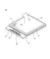
図1は、本発明の第1実施形態に係る表示装置10Aの概略構成を示す斜視図である。
<First Embodiment>
FIG. 1 is a perspective view showing a schematic configuration of a
本実施形態に係る表示装置10Aは、第1基板20と、第2基板21と、複数の画素Pと、シール材22と、端子領域23と、接続端子24とを有している。表示装置10Aの種類については特に限定されないが、例えば有機EL表示装置である。
The
第1基板20上には、表示領域25が設けられている。表示領域25には、第1基板20上に、各々が少なくとも一つの発光素子を有する複数の画素Pが配列されている。
A
表示領域25の上面には第1基板20と対向する第2基板21が設けられている。第2基板21は表示領域25を囲むシール材22によって、第1基板20に固定されている。第1基板20に形成された表示領域25は、第2基板21とシール材22によって大気に晒されないように封止されている。このような封止構造により画素Pに設けられる発光素子の劣化を抑制している。
A
第1基板20には、一端部に端子領域23が設けられている。端子領域23は第2基板21の外側に配置されている。端子領域23は、複数の接続端子24によって構成されている。接続端子24には、映像信号を出力する機器や電源などと表示パネル(図1では表示装置10A)とを接続する配線基板が配置される。配線基板と接続する接続端子24の接点は、外部に露出している。第1基板20には接続端子24から入力された映像信号を表示領域25に出力するドライバIC26が設けられている。
The
尚、ドライバIC26は第1基板20上ではなく、第1基板20とは別のフレキシブルプリント基板(FPC)に配置し、このフレキシブルプリント基板を接続端子24に接続しても良い。ドライバIC26を第1基板20に配置しないことで第1基板20の面積に対する表示領域25の面積を大きくするとができる。
The driver IC 26 may be arranged not on the
図2は、本発明の第1実施形態に係る表示装置10Aの第1基板20の概略構成を示す部分断面図である。また、図3は、本発明の第1実施形態に係る表示装置10Aの概略構成を示す部分平面図である。
FIG. 2 is a partial cross-sectional view showing a schematic configuration of a
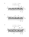
図2に示すように、第1実施形態に係る表示装置10Aは、第1基板20と、第1基板20の主面上に設けられた複数の画素Pと、複数の画素Pを覆うように第1基板20の主面上に設けられた封止膜40とを備える。封止膜40の上には図1に示したシール材22と第2基板21が配置される。
As shown in FIG. 2, the
第1基板20は、複数の画素Pの支持体としての役割を果たすものである。第1基板20の材料としては、ガラス、アクリル樹脂、アルミナ、ポリイミドなどを用いることができる。
The
複数の画素Pは表示装置10Aの主構成要素であり、複数の画素Pの各々は、発光素子30を有している。複数の画素Pの各々は、複数の容量やトランジスタなどをさらに有しているが、図2においてはこれらの図示が省略されている。また、複数の画素Pの各々は、画素P毎に設けられた第1電極31の端部を覆うリブ34によって区画されている。複数の画素Pは、本実施形態においては、図3に示すようにマトリクス状に規則的に配列される。
The plurality of pixels P are the main components of the
発光素子30は、第1電極である陽極31、第2電極である陰極32及びこれらに挟まれるように設けられた発光層33を含む。陽極31は、画素毎に配置される。陽極31は、発光層33で発生した光を陰極側に反射させるため、Ag(銀)等の反射率の高い金属層を用いることが好ましい。陰極32は、複数の画素に共通して配置される。陰極32は、発光層33で発光した光を透過させるため、透光性を有し、且つ導電性を有するITO(酸化スズ添加酸化インジウム)やIZO(酸化インジウム・酸化亜鉛)等の透明導電膜、又は光を透過する金属薄膜を用いることが好ましい。
The
封止膜40は、この順に積層された無機膜41〜44と、無機膜41と42の間に設けられた有機膜51と、無機膜42と43の間に設けられた有機膜52と、無機膜43と44の間に設けられた有機膜53とを含む。特に限定されるものではないが、無機膜41〜44の材料としては、酸化シリコン、窒化シリコン、酸化アルミニウムなど、光透過性であり且つ防水機能の高い無機材料を用いることが好ましい。また、有機膜51〜53の材料としては、透明な紫外線硬化性樹脂などを用いることができる。
The sealing
尚、本実施形態では、4層の無機膜41〜44及びこれらに挟まれた3層の有機膜51〜53によって封止膜40が構成されているが、本発明がこれに限定されるものではなく、少なくとも3層の無機膜及びこれらに挟まれた2層の有機膜を備えていれば足りる。もちろん、5層以上の無機膜及びこれらに挟まれた4層以上の有機膜を備えていても構わない。また、各無機膜は、単層である必要はなく、複数の無機材料からなる積層膜を用いても構わない。
In the present embodiment, the sealing
図2に示すように、無機膜41は、リブ34によって形成される凹凸表面を覆っている。しかしながら、その無機膜41の膜厚は非常に薄いため、無機膜41の表面形状はリブ34の凹凸形状をそのまま反映したものとなる。
As shown in FIG. 2, the
有機膜51は無機膜41の表面に設けられ、その凹凸形状を平坦化する。したがって、有機膜51の上面は実質的に平坦である。図2に示すように、有機膜51は隔壁61によって横方向(以下、平面方向という)に複数の領域に分割されている。本実施形態においては、隔壁61を平面視した時の位置(以下、平面位置という)が所定のリブ34の平面位置と一致している。図3に示すように、隔壁61は、x方向に2画素、y方向に4画素からなるブロックが一単位となるよう、画素の境界である所定のリブ34に沿って設けられ、リブ34上で無機膜41と接触している。隔壁61によって定義されるブロックは、図3に示すように千鳥配置される。
The
無機膜42は有機膜51を覆うとともに、その一部が隔壁61を構成する。隔壁61が形成される平面位置においては、無機膜42にある程度の段差が形成される。
The
有機膜52は無機膜42の表面に設けられ、その凹凸形状を平坦化する。図2に示すように、有機膜52は、隔壁62によって平面方向に複数の領域に分割されている。本実施形態においては、隔壁62の平面位置が別のリブ34の平面位置と一致している。図3に示すように、隔壁62は、x方向に2画素、y方向に4画素からなるブロックが一単位となるよう、画素の境界である別のリブ34に沿って設けられている。隔壁62によって定義されるブロックは、図3に示すように千鳥配置され、その一部は隔壁61によって定義される下層のブロックと平面視で重なっている。本実施形態においては、隔壁61の平面位置に対して隔壁62の平面位置がx方向及びy方向に1画素分シフトしている。
The
無機膜43は有機膜52を覆うとともに、その一部が隔壁62を構成する。隔壁62が形成される平面位置においては、無機膜43にある程度の段差が形成される。
The
有機膜53は無機膜43の表面に設けられ、その凹凸形状を平坦化する。図2に示すように、有機膜53は、隔壁63によって平面方向に複数の領域に分割されている。本実施形態においては、隔壁63の平面位置と隔壁61の平面位置が一致している。図3に示すように、隔壁63は、x方向に2画素、y方向に4画素からなるブロックが一単位となるよう、隔壁61と同じ平面位置に配置される。したがって、隔壁63によって定義されるブロックの平面位置は、隔壁61によって定義されるブロックと同じ平面位置となる。
The
無機膜44は有機膜53を覆うとともに、その一部が隔壁63を構成する。無機膜44は、封止膜40の最上層を構成する膜である。
The
このように、封止膜40は、無機膜41〜44と有機膜51〜53が交互に積層された構造を有していることから、無機膜41〜44によって水分の侵入が防止されるとともに、有機膜51〜53によって平坦性が確保される。このため、異物や段差に起因して生じる無機膜の欠陥が上層まで引き継がれることがなくなる。さらに、本実施形態においては、隔壁61〜63によって有機膜51〜53がそれぞれ複数の領域に分割されている。このような構成を有することによって、無機膜41〜44の全てに欠陥が存在する場合であっても、隔壁61〜63が水分の侵入経路を遮断する役割を果たすため、発光素子30への水分の侵入経路を、確率的に大幅に低減することが可能となる。
As described above, since the sealing
例えば、図2に示すように、無機膜41〜44にそれぞれ欠陥41X〜44Xが存在する場合であっても、有機膜51〜53が隔壁61〜63によって分断されている結果、発光素子30に達する侵入経路は形成されない。図2に示す例では、2番目の有機膜52の所定ブロックまで水分が到達しうるが、当該ブロックの底部は無機膜42の無欠陥部分で覆われているため、水分の侵入はここでストップし、より下層の有機膜51に水分が侵入することがなくなる。
For example, as shown in FIG. 2, even when
特に、表示領域25内に、無機膜によりブロック化した有機膜を上下左右に複数配置したことで、画素Pへの水分の侵入を防止することが可能となる。
In particular, by arranging a plurality of organic films blocked by an inorganic film vertically and horizontally in the
ここで、水分の侵入経路をより確実に遮断するためには、隔壁61〜63をより多く形成することによって、有機膜51〜53をより細かく分割することが好ましい。しかしながら、有機膜51〜53を画素Pのサイズ未満まで分割すると、多数の隔壁61〜63が画素Pと平面視で重なるため、輝度の低下を招くおそれがある。この点を考慮すれば、隔壁61〜63による有機膜51〜53の分割サイズは、画素Pのサイズ以上とすることが好ましい。
Here, in order to more reliably block the invasion route of water, it is preferable to divide the
第1実施形態による表示装置10Aにおいては、隔壁61〜63が画素Pの境界であるリブ34に沿って設けられていることから、隔壁61〜63と画素Pが重ならない。このため、隔壁61〜63の存在による輝度の低下を防止することができる。
In the
尚、本実施形態においては、隔壁61と隔壁63が同じ平面位置に形成され、隔壁62が隔壁61,63と異なる平面位置に形成されているが、本発明がこれに限定されるものではない。例えば、隔壁61、62及び63を全て異なる平面位置に形成しても構わないし、隔壁61、62及び63を全て同じ平面位置に形成しても構わない。さらに、隔壁61、62及び63によって分割される有機膜51〜53の各領域の形状やサイズが一定である必要もない。
In the present embodiment, the
次に、封止膜40の製造方法について説明する。
Next, a method for manufacturing the sealing
まず、図4(a)に示すように、複数の発光素子30を覆うように無機膜41を成膜した後、隔壁61を形成すべき溝領域61aを除く全面に紫外線硬化性樹脂51aを塗布する。無機膜41の成膜方法としては、例えばCVD法など、カバレッジ性の高い成膜方法を用いることが好ましい。以降に形成する無機膜42〜44の成膜方法についても同様である。
First, as shown in FIG. 4A, after forming an
一方、紫外線硬化性樹脂51aの形成方法としては、スクリーン印刷法、オフセット印刷法、インクジェット印刷法、ディスペンス法などを用いて、所望の領域に選択的に塗布することができる。或いは、全面に紫外線硬化性樹脂51aを形成した後、フォトリソグラフィー法を用いたパターニングにより、溝領域61aに対応する部分の紫外線硬化性樹脂51aを除去しても構わない。その後、紫外線UVを照射することによって紫外線硬化性樹脂51aを硬化させれば、溝領域61aを除く全面が有機膜51で覆われた状態となる。
On the other hand, as a method for forming the ultraviolet
次に、図4(b)に示すように、有機膜51の全面に無機膜42を成膜する。無機膜42を成膜すると、溝領域61aに無機膜42の材料が充填されるため、無機膜42と同じ材料によって隔壁61が形成されることになる。隔壁61の底部は無機膜41の上面と接しており、これにより、隔壁61によって分割された有機膜51の各領域は、底面が無機膜41によって覆われ、上面が無機膜42によって覆われ、側面が隔壁61によって覆われた状態となる。
Next, as shown in FIG. 4B, an
その後は、上記工程を繰り返すことにより有機膜52、無機膜43、有機膜53、無機膜44をこの順に形成すればよい。
After that, the
つまり、図4(c)に示すように、隔壁62を形成すべき溝領域62aを除く無機膜42の全面に紫外線硬化性樹脂52aを塗布し、紫外線UVを照射することによって紫外線硬化性樹脂52aを硬化させれば、溝領域62aを除く全面が有機膜52で覆われる。次に、図5(a)に示すように、有機膜52の全面に無機膜43を成膜すれば、溝領域62aに無機膜43の材料が充填されるため、無機膜43と同じ材料によって隔壁62が形成される。隔壁62の底部は無機膜42の上面と接しており、これにより、隔壁62によって分割された有機膜52の各領域は、底面が無機膜42によって覆われ、上面が無機膜43によって覆われ、側面が隔壁62によって覆われた状態となる。
That is, as shown in FIG. 4C, the ultraviolet
さらに、図5(b)に示すように、隔壁63を形成すべき溝領域63aを除く無機膜43の全面に紫外線硬化性樹脂53aを塗布し、紫外線UVを照射することによって紫外線硬化性樹脂53aを硬化させれば、溝領域63aを除く全面が有機膜53で覆われる。そして、図5(c)に示すように、有機膜53の全面に無機膜44を成膜すれば、溝領域63aに無機膜44の材料が充填されるため、無機膜44と同じ材料によって隔壁63が形成される。隔壁63の底部は無機膜43の上面と接しており、これにより、隔壁63によって分割された有機膜53の各領域は、底面が無機膜43によって覆われ、上面が無機膜44によって覆われ、側面が隔壁63によって覆われた状態となる。
Further, as shown in FIG. 5B, the ultraviolet
これにより、複数の発光素子30を覆う封止膜40が完成する。以上の工程によれば、有機膜となる紫外線硬化性樹脂51a〜53aに溝領域61a〜63aを設けるだけで、隔壁61〜63を形成することができることから、製造工程が大幅に複雑化することはない。
As a result, the sealing
しかも、本実施形態においては、上下に隣接する2つの隔壁、つまり隔壁61と隔壁62や、隔壁62と隔壁63の平面位置が互いに異なっていることから、隔壁61、62によって生じる凹凸が上層の有機膜52、53によって平坦化される。このため、凹凸に起因した無機膜42〜44の欠陥を防止することも可能となる。
Moreover, in the present embodiment, since the plane positions of the two partition walls adjacent to each other, that is, the
<第2実施形態>
図6は、第2実施形態による表示装置10Bの概略構成を示す部分断面図である。
<Second Embodiment>
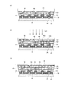
FIG. 6 is a partial cross-sectional view showing a schematic configuration of the
第2実施形態による表示装置10Bは、無機膜45及び有機膜54が追加されている点において、図2に示した表示装置10Aと相違している。その他の構成については、図2に示した表示装置10Aと同一であることから、重複する説明は省略する。
The
図6に示すように、有機膜54は、無機膜41と無機膜45との間に設けられ、リブ34によって区画された画素領域を埋め込むように設けられている。有機膜54の上面は、リブ34の上面とほぼ同一平面を構成することが好ましく、この場合、無機膜45はほぼ平坦となる。これによれば、有機膜51の膜厚をほぼ一定とすることができることから、有機膜51の形成が容易となる。
As shown in FIG. 6, the
有機膜54の形成方法としては、インクジェット印刷法を用いることが好ましい。インクジェット印刷法を用いる場合、使用する樹脂材料の粘度がある程度低い必要があるが、リブ34によって樹脂材料の流動が抑えられるため、インクジェット印刷法を用いて所望の領域に有機膜54を選択的に形成することが可能である。したがって、有機膜54については、他の有機膜51〜53とは異なる、インクジェット印刷法に適した樹脂材料を用いることができる。
As a method for forming the
<第3施形態>
図7は、第3実施形態による表示装置10Cの概略構成を示す部分平面図である。
<Third embodiment>
FIG. 7 is a partial plan view showing a schematic configuration of the display device 10C according to the third embodiment.
図7に示すように、第3実施形態による表示装置10Cは、隔壁61〜63が斜め方向に延在している点において、第1実施形態による表示装置10Aと相違している。その他の構成については、図3に示した表示装置10Aと同一であることから、重複する説明は省略する。
As shown in FIG. 7, the display device 10C according to the third embodiment is different from the
本実施形態においては、隔壁61〜63の延在方向をAとした場合、リブ34の延在方向であるx方向に対して、隔壁61〜63の延在方向Aが角度θだけ傾いている。角度θは、例えば30°である。
In the present embodiment, when the extending direction of the
本実施形態によれば、画素Pの規則性と隔壁61〜63の規則性との間に相関がなくなることから、プロセスばらつきなどによって隔壁61〜63の形成位置に多少のずれが生じたとしても、モアレ縞が発生しにくくなる。尚、図7に示した例では、隔壁61〜63をいずれも同方向に傾けているが、隔壁61〜63をそれぞれ異なる傾きとしても構わない。これによれば、隔壁61〜63間の干渉によるモアレ縞の発生を防止することも可能となる。
According to the present embodiment, since there is no correlation between the regularity of the pixels P and the regularity of the
<第4実施形態>
図8は、第4実施形態による表示装置10Dの概略構成を示す部分断面図である。また、図9は、第4実施形態による表示装置10Dの概略構成を示す部分平面図である。
<Fourth Embodiment>
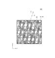
FIG. 8 is a partial cross-sectional view showing a schematic configuration of the
第4実施形態による表示装置10Dは、隔壁61〜63の形成位置がランダムである点において、図2及び図3に示した表示装置10Aと相違している。その他の構成については、図2及び図3に示した表示装置10Aと同一であることから、重複する説明は省略する。
The
本実施形態においては、隔壁61〜63がランダムに形成されていることから、隔壁61〜63によって分割される有機膜51〜53の各領域のサイズはまちまちとなる。このため、例えば同じ有機膜51においても、互いに平面サイズの異なる領域が存在することになる。ランダム形状の具体例としては、図9に示すように、サイズの異なる複数の円又は楕円が平面視で重なるようなパターンを用いることができる。
In the present embodiment, since the
本実施形態においても、画素Pの規則性と隔壁61〜63の規則性との間に相関がなくなることから、モアレ縞の発生を防止することができる。しかも、隔壁61〜63間における相関もほとんどないことから、隔壁61〜63間の干渉によるモアレ縞の発生を防止することもできる。
Also in this embodiment, since there is no correlation between the regularity of the pixels P and the regularity of the
以上、本発明のいくつかの実施形態について説明したが、本発明は、上記の実施形態に限定されることなく、本発明の主旨を逸脱しない範囲で種々の変更が可能であり、それらも本発明の範囲内に包含されるものであることはいうまでもない。 Although some embodiments of the present invention have been described above, the present invention is not limited to the above embodiments, and various modifications can be made without departing from the gist of the present invention. Needless to say, it is included in the scope of the invention.
10A〜10D:表示装置 20:第1基板 21:第2基板 22:シール材 23:端子領域 24:接続端子 25:表示領域 26:ドライバIC 30:発光素子 31:陽極 32:陰極 33:発光層 34:リブ 40:封止膜 41〜45:無機膜 41X〜44X:欠陥 51〜54:有機膜 51a〜53a:紫外線硬化性樹脂 61〜63:隔壁 61a〜63a:溝領域 P:画素 UV:紫外線
10A-10D: Display device 20: 1st substrate 21: 2nd substrate 22: Sealing material 23: Terminal area 24: Connection terminal 25: Display area 26: Driver IC 30: Light emitting element 31: Anode 32: Cathode 33: Light emitting layer 34: Ribs 40: Encapsulating film 41-45:
Claims (11)
前記複数の画素を覆うように前記基板上に設けられた封止膜と、
を備え、
前記複数の画素はそれぞれ、第1電極と、第2電極と、前記第1電極及び前記第2電極に接して挟まれる有機層と、を有する発光素子を有し、
前記封止膜は、積層された第1、第2及び第3の無機膜と、前記第1の無機膜と前記第2の無機膜との間に配置された第1の有機膜と、前記第2の無機膜と前記第3の無機膜との間に配置された第2の有機膜とを含み、
前記第1の有機膜は、第1の隔壁によって複数の領域に分割され、
前記第2の有機膜は、第2の隔壁によって複数の領域に分割され、
前記第1の有機膜の複数の領域はそれぞれ、第1部分と第2部分と、を有し、
前記第2の有機膜の複数の領域はそれぞれ、平面視で前記第1部分と重畳するとともに前記第2部分と重畳しない第3部分を有し、
前記第1の隔壁及び前記第2の隔壁はそれぞれ、平面視で前記発光素子と重畳しないように設けられていることを特徴とする表示装置。 With multiple pixels provided on the board,
A sealing film provided on the substrate so as to cover the plurality of pixels,
With
Each of the plurality of pixels has a light emitting element having a first electrode, a second electrode, and an organic layer sandwiched in contact with the first electrode and the second electrode.
The sealing film includes a laminated first, second and third inorganic film, a first organic film arranged between the first inorganic film and the second inorganic film, and the above. Includes a second organic film disposed between the second inorganic film and the third inorganic film.
The first organic film is divided into a plurality of regions by a first partition wall, and the first organic film is divided into a plurality of regions .
The second organic film is divided into a plurality of regions by a second partition wall, and is divided into a plurality of regions .
Each of the plurality of regions of the first organic film has a first portion and a second portion, respectively.
Each of the plurality of regions of the second organic film has a third portion that overlaps with the first portion and does not overlap with the second portion in a plan view.
A display device characterized in that the first partition wall and the second partition wall are each provided so as not to overlap with the light emitting element in a plan view .
前記第1の隔壁は、前記リブに沿って設けられていることを特徴とする請求項4に記載の表示装置。 A rib that covers the end of the first electrode and exposes a part of the upper surface thereof to partition the light emitting element is further provided.
The display device according to claim 4, wherein the first partition wall is provided along the rib.
前記第1及び第2の隔壁の少なくとも一方は、平面視で前記複数の画素の境界の延びる方向に対して所定の角度だけ傾斜して延在することを特徴とする請求項1に記載の表示装置。 The plurality of pixels are regularly arranged and
The display according to claim 1, wherein at least one of the first and second partition walls is inclined by a predetermined angle with respect to the extending direction of the boundary of the plurality of pixels in a plan view. apparatus.
Priority Applications (6)
| Application Number | Priority Date | Filing Date | Title |
|---|---|---|---|
| JP2016053469A JP6792950B2 (en) | 2016-03-17 | 2016-03-17 | Display device |
| US15/372,446 US9865843B2 (en) | 2016-03-17 | 2016-12-08 | Display device |
| KR1020160166501A KR20170108791A (en) | 2016-03-17 | 2016-12-08 | Display device |
| TW105141216A TWI617864B (en) | 2016-03-17 | 2016-12-13 | Display device |
| CN201611144572.2A CN107204403B (en) | 2016-03-17 | 2016-12-13 | Display device |
| KR1020180076364A KR101937613B1 (en) | 2016-03-17 | 2018-07-02 | Display device |
Applications Claiming Priority (1)
| Application Number | Priority Date | Filing Date | Title |
|---|---|---|---|
| JP2016053469A JP6792950B2 (en) | 2016-03-17 | 2016-03-17 | Display device |
Publications (3)
| Publication Number | Publication Date |
|---|---|
| JP2017168348A JP2017168348A (en) | 2017-09-21 |
| JP2017168348A5 JP2017168348A5 (en) | 2019-04-25 |
| JP6792950B2 true JP6792950B2 (en) | 2020-12-02 |
Family
ID=59856043
Family Applications (1)
| Application Number | Title | Priority Date | Filing Date |
|---|---|---|---|
| JP2016053469A Active JP6792950B2 (en) | 2016-03-17 | 2016-03-17 | Display device |
Country Status (5)
| Country | Link |
|---|---|
| US (1) | US9865843B2 (en) |
| JP (1) | JP6792950B2 (en) |
| KR (2) | KR20170108791A (en) |
| CN (1) | CN107204403B (en) |
| TW (1) | TWI617864B (en) |
Families Citing this family (9)
| Publication number | Priority date | Publication date | Assignee | Title |
|---|---|---|---|---|
| KR101984669B1 (en) * | 2017-09-26 | 2019-05-31 | 삼성중공업 주식회사 | LNG regasification system for ship |
| JP6983084B2 (en) * | 2018-02-07 | 2021-12-17 | 株式会社ジャパンディスプレイ | Organic EL display device |
| CN108461645A (en) * | 2018-02-09 | 2018-08-28 | 武汉华星光电半导体显示技术有限公司 | A kind of encapsulating structure and preparation method on flexible display device |
| US11296156B2 (en) * | 2018-11-28 | 2022-04-05 | Lg Display Co., Ltd. | Organic light emitting diode device |
| CN109698212B (en) * | 2018-12-28 | 2020-11-06 | 上海集成电路研发中心有限公司 | Manufacturing method of pixel array layout and manufacturing method of pixel array |
| US11258045B2 (en) | 2019-11-27 | 2022-02-22 | Applied Materials, Inc. | Methods of forming stretchable encapsulation for electronic displays |
| US11211439B2 (en) * | 2019-11-27 | 2021-12-28 | Applied Materials, Inc. | Stretchable polymer and dielectric layers for electronic displays |
| US11362307B2 (en) | 2019-11-27 | 2022-06-14 | Applied Materials, Inc. | Encapsulation having polymer and dielectric layers for electronic displays |
| CN111326677B (en) * | 2020-03-09 | 2023-05-26 | 京东方科技集团股份有限公司 | Display device, display panel and packaging method of display substrate |
Family Cites Families (15)
| Publication number | Priority date | Publication date | Assignee | Title |
|---|---|---|---|---|
| US6866901B2 (en) | 1999-10-25 | 2005-03-15 | Vitex Systems, Inc. | Method for edge sealing barrier films |
| US20070196682A1 (en) * | 1999-10-25 | 2007-08-23 | Visser Robert J | Three dimensional multilayer barrier and method of making |
| JP4643138B2 (en) * | 2003-11-27 | 2011-03-02 | 東芝モバイルディスプレイ株式会社 | Display device and manufacturing method thereof |
| US20100155709A1 (en) * | 2007-05-24 | 2010-06-24 | Koninklijke Philips Electronics N.V. | Encapsulation for an electronic thin film device |
| JP4977548B2 (en) | 2007-07-31 | 2012-07-18 | 住友化学株式会社 | Organic electroluminescence device and manufacturing method thereof |
| JP5024220B2 (en) | 2008-07-24 | 2012-09-12 | セイコーエプソン株式会社 | ORGANIC ELECTROLUMINESCENT DEVICE, METHOD FOR PRODUCING ORGANIC ELECTROLUMINESCENT DEVICE, ELECTRONIC DEVICE |
| EP2346020A4 (en) | 2008-10-02 | 2014-12-31 | Sharp Kk | Display device substrate, display device substrate manufacturing method, display device, liquid crystal display (lcd) device, lcd manufacturing method, and organic electroluminescence display device |
| KR101261456B1 (en) * | 2010-12-29 | 2013-05-10 | 순천향대학교 산학협력단 | Protective thin film and electronic devices comprising the same |
| KR101952445B1 (en) * | 2012-05-10 | 2019-04-26 | 리쿠아비스타 비.브이. | Eloctro wetting display apparatus |
| EP2698836A1 (en) * | 2012-08-17 | 2014-02-19 | Nederlandse Organisatie voor toegepast -natuurwetenschappelijk onderzoek TNO | Foil, electro-optic component and method of manufacturing these |
| TWI501441B (en) * | 2012-08-24 | 2015-09-21 | Ind Tech Res Inst | Discontinuous compound barrier layer, method for forming the same and package using the same |
| KR101589884B1 (en) * | 2012-09-04 | 2016-01-28 | 샤프 가부시키가이샤 | Organic electroluminescent display, and production method therefor |
| CN103022354B (en) * | 2012-12-28 | 2016-05-11 | 昆山工研院新型平板显示技术中心有限公司 | A kind of flexible substrate |
| KR102047006B1 (en) * | 2013-06-07 | 2019-12-03 | 삼성디스플레이 주식회사 | Organic luminescence emitting display device |
| US9287522B2 (en) * | 2013-07-30 | 2016-03-15 | Global Oled Technology Llc | Local seal for encapsulation of electro-optical element on a flexible substrate |
-
2016
- 2016-03-17 JP JP2016053469A patent/JP6792950B2/en active Active
- 2016-12-08 US US15/372,446 patent/US9865843B2/en active Active
- 2016-12-08 KR KR1020160166501A patent/KR20170108791A/en active Search and Examination
- 2016-12-13 TW TW105141216A patent/TWI617864B/en active
- 2016-12-13 CN CN201611144572.2A patent/CN107204403B/en active Active
-
2018
- 2018-07-02 KR KR1020180076364A patent/KR101937613B1/en active IP Right Grant
Also Published As
| Publication number | Publication date |
|---|---|
| CN107204403A (en) | 2017-09-26 |
| US9865843B2 (en) | 2018-01-09 |
| CN107204403B (en) | 2019-05-10 |
| TWI617864B (en) | 2018-03-11 |
| JP2017168348A (en) | 2017-09-21 |
| KR20180081681A (en) | 2018-07-17 |
| US20170271619A1 (en) | 2017-09-21 |
| KR20170108791A (en) | 2017-09-27 |
| TW201734592A (en) | 2017-10-01 |
| KR101937613B1 (en) | 2019-01-10 |
Similar Documents
| Publication | Publication Date | Title |
|---|---|---|
| JP6792950B2 (en) | Display device | |
| JP6756538B2 (en) | Display device | |
| TWI634468B (en) | Transparent display device | |
| JP6673631B2 (en) | Array substrate | |
| JP4816985B2 (en) | Organic EL display device | |
| JP5676554B2 (en) | Organic light emitting display | |
| US20190312092A1 (en) | Flexible display device | |
| KR101695082B1 (en) | Display device | |
| JP5541984B2 (en) | Organic EL display device | |
| JP6785627B2 (en) | Display device | |
| JP6663249B2 (en) | Display device | |
| US10367047B2 (en) | Display device | |
| JP6692194B2 (en) | Display device | |
| KR102495122B1 (en) | Display device | |
| KR102582066B1 (en) | Chip on film package and display device including the chip on film package | |
| KR20210002283A (en) | Display apparatus and Method of manufacturing of the same | |
| US20210249631A1 (en) | Display device and manufacturing method thereof | |
| KR20170096090A (en) | Display device | |
| KR101778364B1 (en) | Display device | |
| TWI638299B (en) | Display device and manufacturing method thereof | |
| US20170358631A1 (en) | Display device | |
| JP2017096998A (en) | Display device | |
| KR20210028773A (en) | Display device | |
| US10978521B2 (en) | Display device | |
| KR100552959B1 (en) | Substrate containing the black matrix and fabricating the same and FPD using the same |
Legal Events
| Date | Code | Title | Description |
|---|---|---|---|
| A521 | Request for written amendment filed |
Free format text: JAPANESE INTERMEDIATE CODE: A523 Effective date: 20190313 |
|
| A621 | Written request for application examination |
Free format text: JAPANESE INTERMEDIATE CODE: A621 Effective date: 20190313 |
|
| A977 | Report on retrieval |
Free format text: JAPANESE INTERMEDIATE CODE: A971007 Effective date: 20200210 |
|
| A131 | Notification of reasons for refusal |
Free format text: JAPANESE INTERMEDIATE CODE: A131 Effective date: 20200310 |
|
| A601 | Written request for extension of time |
Free format text: JAPANESE INTERMEDIATE CODE: A601 Effective date: 20200508 |
|
| A521 | Request for written amendment filed |
Free format text: JAPANESE INTERMEDIATE CODE: A523 Effective date: 20200515 |
|
| TRDD | Decision of grant or rejection written | ||
| A01 | Written decision to grant a patent or to grant a registration (utility model) |
Free format text: JAPANESE INTERMEDIATE CODE: A01 Effective date: 20201013 |
|
| A61 | First payment of annual fees (during grant procedure) |
Free format text: JAPANESE INTERMEDIATE CODE: A61 Effective date: 20201109 |
|
| R150 | Certificate of patent or registration of utility model |
Ref document number: 6792950 Country of ref document: JP Free format text: JAPANESE INTERMEDIATE CODE: R150 |
|
| R250 | Receipt of annual fees |
Free format text: JAPANESE INTERMEDIATE CODE: R250 |