EP1432136A2 - Rauschfilter - Google Patents
Rauschfilter Download PDFInfo
- Publication number
- EP1432136A2 EP1432136A2 EP03255174A EP03255174A EP1432136A2 EP 1432136 A2 EP1432136 A2 EP 1432136A2 EP 03255174 A EP03255174 A EP 03255174A EP 03255174 A EP03255174 A EP 03255174A EP 1432136 A2 EP1432136 A2 EP 1432136A2
- Authority
- EP
- European Patent Office
- Prior art keywords
- signal lines
- signal
- medium
- mode signal
- mode
- Prior art date
- Legal status (The legal status is an assumption and is not a legal conclusion. Google has not performed a legal analysis and makes no representation as to the accuracy of the status listed.)
- Withdrawn
Links
- 230000005540 biological transmission Effects 0.000 claims abstract description 77
- 230000035699 permeability Effects 0.000 claims abstract description 53
- 239000000463 material Substances 0.000 claims description 46
- 230000005672 electromagnetic field Effects 0.000 claims description 30
- 239000011248 coating agent Substances 0.000 claims description 12
- 238000000576 coating method Methods 0.000 claims description 12
- 239000000696 magnetic material Substances 0.000 claims description 10
- 239000003989 dielectric material Substances 0.000 claims description 4
- 239000011810 insulating material Substances 0.000 claims description 2
- 230000002238 attenuated effect Effects 0.000 abstract description 15
- 230000004907 flux Effects 0.000 description 23
- 239000007769 metal material Substances 0.000 description 22
- 230000001965 increasing effect Effects 0.000 description 17
- 229910000859 α-Fe Inorganic materials 0.000 description 13
- 230000003247 decreasing effect Effects 0.000 description 10
- 238000010304 firing Methods 0.000 description 6
- 238000010586 diagram Methods 0.000 description 5
- 230000001629 suppression Effects 0.000 description 5
- KDLHZDBZIXYQEI-UHFFFAOYSA-N Palladium Chemical compound [Pd] KDLHZDBZIXYQEI-UHFFFAOYSA-N 0.000 description 4
- 230000002708 enhancing effect Effects 0.000 description 4
- 238000000034 method Methods 0.000 description 4
- 238000012986 modification Methods 0.000 description 4
- 230000004048 modification Effects 0.000 description 4
- 239000011347 resin Substances 0.000 description 4
- 229920005989 resin Polymers 0.000 description 4
- 239000000758 substrate Substances 0.000 description 4
- 230000001747 exhibiting effect Effects 0.000 description 3
- 230000001902 propagating effect Effects 0.000 description 3
- 239000004642 Polyimide Substances 0.000 description 2
- BQCADISMDOOEFD-UHFFFAOYSA-N Silver Chemical compound [Ag] BQCADISMDOOEFD-UHFFFAOYSA-N 0.000 description 2
- 239000003990 capacitor Substances 0.000 description 2
- 239000000919 ceramic Substances 0.000 description 2
- 229910010293 ceramic material Inorganic materials 0.000 description 2
- 239000002131 composite material Substances 0.000 description 2
- 239000004020 conductor Substances 0.000 description 2
- 238000010030 laminating Methods 0.000 description 2
- 238000004519 manufacturing process Methods 0.000 description 2
- 239000000203 mixture Substances 0.000 description 2
- 229910052763 palladium Inorganic materials 0.000 description 2
- 230000002093 peripheral effect Effects 0.000 description 2
- 229920001721 polyimide Polymers 0.000 description 2
- 229910052709 silver Inorganic materials 0.000 description 2
- 239000004332 silver Substances 0.000 description 2
- XEEYBQQBJWHFJM-UHFFFAOYSA-N Iron Chemical compound [Fe] XEEYBQQBJWHFJM-UHFFFAOYSA-N 0.000 description 1
- 229910018605 Ni—Zn Inorganic materials 0.000 description 1
- PNEYBMLMFCGWSK-UHFFFAOYSA-N aluminium oxide Inorganic materials [O-2].[O-2].[O-2].[Al+3].[Al+3] PNEYBMLMFCGWSK-UHFFFAOYSA-N 0.000 description 1
- 230000008859 change Effects 0.000 description 1
- 230000008878 coupling Effects 0.000 description 1
- 238000010168 coupling process Methods 0.000 description 1
- 238000005859 coupling reaction Methods 0.000 description 1
- 238000006073 displacement reaction Methods 0.000 description 1
- 238000009826 distribution Methods 0.000 description 1
- 230000005684 electric field Effects 0.000 description 1
- 239000011521 glass Substances 0.000 description 1
- 238000004898 kneading Methods 0.000 description 1
- 239000006247 magnetic powder Substances 0.000 description 1
- 239000000843 powder Substances 0.000 description 1
- 238000003825 pressing Methods 0.000 description 1
- 230000005855 radiation Effects 0.000 description 1
Images


Classifications
-
- H—ELECTRICITY
- H01—ELECTRIC ELEMENTS
- H01P—WAVEGUIDES; RESONATORS, LINES, OR OTHER DEVICES OF THE WAVEGUIDE TYPE
- H01P1/00—Auxiliary devices
- H01P1/20—Frequency-selective devices, e.g. filters
- H01P1/201—Filters for transverse electromagnetic waves
- H01P1/203—Strip line filters
-
- H—ELECTRICITY
- H01—ELECTRIC ELEMENTS
- H01P—WAVEGUIDES; RESONATORS, LINES, OR OTHER DEVICES OF THE WAVEGUIDE TYPE
- H01P1/00—Auxiliary devices
- H01P1/22—Attenuating devices
- H01P1/23—Attenuating devices using ferromagnetic material
-
- H—ELECTRICITY
- H01—ELECTRIC ELEMENTS
- H01P—WAVEGUIDES; RESONATORS, LINES, OR OTHER DEVICES OF THE WAVEGUIDE TYPE
- H01P1/00—Auxiliary devices
- H01P1/20—Frequency-selective devices, e.g. filters
- H01P1/201—Filters for transverse electromagnetic waves
- H01P1/203—Strip line filters
- H01P1/20327—Electromagnetic interstage coupling
- H01P1/20336—Comb or interdigital filters
- H01P1/20345—Multilayer filters
-
- H—ELECTRICITY
- H01—ELECTRIC ELEMENTS
- H01P—WAVEGUIDES; RESONATORS, LINES, OR OTHER DEVICES OF THE WAVEGUIDE TYPE
- H01P1/00—Auxiliary devices
- H01P1/22—Attenuating devices
- H01P1/227—Strip line attenuators
Definitions
- the present invention relates to noise filters suitable for use in electronic circuits utilizing differential signals, such as in high-speed differential interfaces.
- an electronic circuit utilizing differential signals is formed of two differential lines. Due to various reasons, common-mode noise (common-mode signal), which causes the radiation of electromagnetic noise, disadvantageously flows in such differential lines. Accordingly, a common-mode choke coil is connected to a mid-portion of the differential lines as a noise filter so as to allow the normal-mode signal to pass through and to reflect the common-mode signal, thereby eliminating common-mode noise.
- noise is suppressed by reflection loss. Accordingly, if a noise filter is disposed in a mid-portion of the lines connecting circuits, noise having a specific frequency may sometimes resonate between the noise filter and a peripheral circuit, which increases the noise in spite of the provision of the noise filter.
- the signal frequency used in digital devices is becoming higher, and there is an increased number of electronic devices using signal frequencies of 100 MHz or higher.
- the frequency of common-mode noise is also becoming higher, and the line length between the noise filter and a peripheral component or the line length between a plurality of components thus becomes vulnerable to the noise.
- noise filters noise cannot be sufficiently eliminated due to the influence of the resonant frequency caused by the reflection, and signal waveforms become distorted.
- noise filters that eliminate noise by utilizing reflection loss cannot be employed.
- a noise filter formed by using a chip coil in which two lines are embedded in a medium, for example, in ferrite.
- the attenuation (permeability) ratio for one of the common-mode signal and the normal-mode signal is determined, the attenuation ratio for the other mode signal is also determined since the two lines are disposed in the medium, which is uniform. It is thus difficult to set the attenuation ratio for each of the mode signals.
- the invention provides in various aspects a small noise filter in which the attenuation ratio for each of the mode signals can be set while preventing resonance noise.
- a noise filter comprising: a transmission line which includes an insulating medium formed of an insulating material, two signal lines provided for the insulating medium with a spacing therebetween, and a ground electrode, wherein, between a common-mode signal in which the directions of currents flowing in the two signal lines are the same and a normal-mode signal in which the directions of currents flowing in the two signal lines are different, one of the common-mode signal and the normal-mode signal, which is not desired, is eliminated; and an additional medium which is made of a material different from the insulating medium is disposed at a position in the presence of only one of an electromagnetic field substantially generated by the common-mode signal and an electromagnetic field substantially generated by the normal-mode signal, thereby adjusting loss of the common-mode signal or the normal-mode signal for which the additional medium is disposed.
- the signals propagate in the transmission line via the insulating medium so that they can be attenuated by utilizing thermal loss in the insulating medium. Since the two signal lines are disposed side by side with a spacing therebetween, the electromagnetic fields generated by the signals in the signal lines mutually influence each other between the signal lines. Accordingly, the electromagnetic field distribution formed in the insulating medium is different between the common mode and the normal mode, and thus, the attenuation of the common-mode signal and the attenuation of the normal-mode signal also become different.
- An additional medium which is made of a material different from the insulating medium is disposed at a position in the presence of only one of the electromagnetic field substantially generated by the common-mode signal and the electromagnetic field substantially generated by the normal-mode signal.
- the effective material characteristics can be changed between the modes.
- the attenuation for each of the mode signals can be adjusted, and the loss of the signal of the desired mode can be decreased, while the loss of the signal of the undesired mode can be increased.
- the frequency characteristics of the effective relative magnetic permeability for the signal of the desired mode can be changed. Accordingly, for the signal of the desired mode, the frequency at which the loss peaks can be shifted to a higher frequency range.
- the signal of the undesired mode can be removed in a low frequency range, and the signal of the desired mode can pass through the filter without being attenuated up to the high frequency range and without causing blunt waves.
- a noise filter comprising: a transmission line which includes an insulating medium formed of a plurality of overlaid insulating layers, two signal lines disposed between the corresponding insulating layers with a spacing therebetween, and two ground electrodes sandwiching the corresponding insulating layers including the two signal lines, wherein, between a common-mode signal in which the directions of currents flowing in the two signal lines are the same and a normal-mode signal in which the directions of currents flowing in the two signal lines are different, one of the common-mode signal and the normal-mode signal, which is not desired, is eliminated; and an additional medium which is made of a material different from the insulating medium is disposed at a position in the presence of only one of an electromagnetic field substantially generated by the common-mode signal and an electromagnetic field substantially generated by the normal-mode signal, thereby adjusting loss of the common-mode signal or the normal-mode signal for which the additional medium is disposed.
- the signals propagating in the transmission line can be attenuated by utilizing thermal loss in the insulating layers.
- An additional medium which is made of a material different from the insulating medium is disposed at a position in the presence of only one of the electromagnetic field substantially generated by the common-mode signal and the electromagnetic field substantially generated by the normal-mode signal.
- the normal-mode characteristic impedance of the transmission line can be set by suitably adjusting the widths of the signal lines, the thickness of the insulating layers, the material characteristics, etc. Additionally, the signal lines are disposed between the corresponding insulating layers, and the two ground electrodes sandwich the insulating layers including the two signal lines therebetween. Accordingly, the transmission line can be formed such that the entire length of the signal lines is covered with the ground electrodes. Thus, the common-mode characteristic impedance can be maintained at a constant value over the entire transmission line, thereby preventing noise from being reflected in the transmission line and also preventing noise resonance and the distortion of the waveform. Since the signal lines are entirely covered with the ground electrodes, noise can be prevented from entering the signal lines from the exterior, thereby enhancing the transmission reliability of the signals.
- the normal-mode characteristic impedance and the common-mode characteristic impedance can be individually set. While normal-mode characteristic impedance matching to an external circuit is provided, common-mode characteristic impedance matching to the external circuit may be provided or may not be provided. If common-mode characteristic impedance matching is not provided, noise can be suppressed by utilizing reflection loss. If common-mode characteristic impedance is provided, noise can be suppressed by utilizing thermal loss in the insulating layers while preventing problems, for example, resonance, caused by the reflection.
- the common-mode characteristic impedance can be set independently of the normal-mode characteristic impedance. Accordingly, the transmission loss for the common-mode signal can be increased by utilizing reflection loss and/or thermal loss than that in the related art.
- the configuration of the present invention there is no insertion-loss resonance point in the high frequency range (several hundred megahertz or higher), which is observed in the related art, thereby making it possible to attenuate noise up to about 10 GHz.
- Normal-mode characteristic impedance matching to an external circuit can be provided more easily than the related art, thereby reducing the influence of, for example, resonance, on the waveform of the normal-mode signal.
- a noise filter comprising:
- the signals propagating in the transmission line can be attenuated by utilizing thermal loss in the insulating layers.
- An additional medium which is made of a material different from the insulating medium is disposed at a position in the presence of only one of the electromagnetic field substantially generated by the common-mode signal and the electromagnetic field substantially generated by the normal-mode signal.
- the signal lines can be disposed between the corresponding insulating layers, and also, the entire length of the signal lines can be covered with the two ground electrodes. It is also possible to prevent noise from entering the transmission line from the exterior, thereby enhancing the transmission reliability of the signals.
- the common-mode characteristic impedances of the transmission lines can be substantially the same, and also, the normal-mode characteristic impedances of the transmission lines can be substantially the same. Accordingly, the common-mode characteristic impedance can be maintained substantially at a constant value over the entire transmission lines connected in series with each other. As a result, noise can be prevented from being reflected in the transmission line, and also preventing noise resonance and the distortion of the waveform.
- the normal-mode characteristic impedance and the common-mode characteristic impedance can be individually set. While normal-mode characteristic impedance matching to an external circuit is provided, common-mode characteristic impedance matching to the external circuit may be provided or may not be provided. If common-mode characteristic impedance matching is not provided, noise can be suppressed by utilizing reflection loss. Regardless of whether or not common-mode characteristic impedance is provided, the common-mode characteristic impedance can be set independently of the normal-mode characteristic impedance. Accordingly, the transmission loss for the common-mode signal can be increased by utilizing reflection loss and/or thermal loss than that in the related art.
- the transmission lines are connected in series with each other between the plurality of layers. Accordingly, the overall length of the signal lines can be increased, and the attenuation of noise passing through the signal lines can be increased.
- a noise filter comprising: a transmission line which includes a layered insulating medium, two signal lines disposed on the obverse surface of the insulating medium with a spacing therebetween, and a ground electrode disposed on the reverse surface of the insulating medium, wherein, between a common-mode signal in which the directions of currents flowing in the two signal lines are the same and a normal-mode signal in which the directions of currents flowing in the two signal lines are different, one of the common-mode signal and the normal-mode signal, which is not desired, is eliminated; and an additional medium which is made of a material different from the insulating medium is disposed at a position in the presence of only one of an lectromagnetic field substantially generated by the common-mode signal and an electromagnetic field substantially generated by the normal-mode signal, thereby adjusting loss of the common-mode signal or the normal-mode signal for which the additional medium is disposed.
- the two signal lines are disposed on the obverse surface of the insulating medium, and thus, the signals propagating in the transmission line can be attenuated by utilizing thermal loss in the insulating medium.
- An additional medium which is made of a material different from the insulating medium is disposed at a position in the presence of only one of the electromagnetic field substantially generated by the common-mode signal and the electromagnetic field substantially generated by the normal-mode signal.
- the transmission line can be formed by covering the entire length of the two signal lines with the ground electrode from the reverse surface of the insulating medium.
- the common-mode characteristic impedance can be set to be a constant value over the entire transmission line, thereby preventing noise from being reflected in the transmission line and also preventing noise resonance.
- the normal-mode characteristic impedance and the common-mode characteristic impedance can be individually set. While normal-mode characteristic impedance matching to an external circuit is provided, common-mode characteristic impedance matching to the external circuit may be provided or may not be provided. Regardless of whether or not common-mode characteristic impedance is provided, the common-mode characteristic impedance can be set independently of the normal-mode characteristic impedance. Accordingly, the transmission loss for the common-mode signal can be increased by utilizing reflection loss and/or thermal loss than that in the related art.
- the additional medium may be disposed between the two signal lines.
- the two signal lines are disposed side by side with a spacing therebetween. Accordingly, in the common mode, a magnetic flux which entirely surrounds the two signal lines is formed. In the normal mode, however, magnetic fluxes which individually surround the two signal lines are formed. Thus, in the common mode, a magnetic flux is not formed between the two signal lines. In contrast, in the normal mode, a magnetic flux (magnetic field) which passes through the two signal lines is formed. Therefore, by disposing the additional medium between the two signal lines, only the magnetic fluxes of the normal mode can be adjusted.
- an electric flux (electric field) is formed between the two signal lines and the ground electrode.
- an electric flux connecting the two signal lines is formed. Therefore, by disposing the additional medium between the two signal lines, only the electric flux of the normal mode can be adjusted.
- the additional medium can be disposed at a position through which the magnetic flux or the electric flux of only the normal mode passes, thereby making it possible to adjust the effective relative magnetic permeability or the effective relative dielectric constant of the normal mode.
- the insulating medium may be formed of a magnetic medium made of a magnetic material
- the additional medium may be formed of a non-magnetic medium, a space, or a low-magnetic-permeability medium having a relative magnetic permeability smaller than the magnetic medium.
- the signals can be attenuated by utilizing magnetic loss (thermal loss) of the magnetic medium.
- a low-magnetic-permeability medium having a relative magnetic permeability smaller than the magnetic medium is disposed between the two signal lines.
- the frequency characteristics of the effective relative magnetic permeability for the normal mode, which is a desired mode, can be changed, and the frequency at which the loss peaks can be shifted to a higher frequency range. Accordingly, the common-mode signal can be removed from the low frequency range, and the normal-mode signal can propagate without being attenuated up to the high frequency range.
- the normal-mode signal can be transmitted without causing blunt waves.
- the insulating medium may be formed of a dielectric medium made of a dielectric material.
- An incision groove may be formed between the two signal lines on the obverse surface of the dielectric medium, and the additional medium may be formed of a space defined in the incision groove.
- the signals can be attenuated by utilizing dielectric loss (thermal loss) of the dielectric material.
- dielectric loss thermal loss
- the effective relative magnetic permeability of the normal mode can be decreased by the space defined in the incision groove, thereby making it possible to reduce the loss of the normal-mode signal.
- the insulating medium may be formed of a magnetic medium made of a magnetic material.
- the additional medium may be disposed between the two signal lines and may be formed of a non-magnetic medium, a space, or a low-magnetic-permeability medium having a relative magnetic permeability smaller than the magnetic medium, and a coating film having a relative magnetic permeability higher than the additional medium may cover the additional medium and the two signal lines.
- the signals can be attenuated by utilizing magnetic loss (thermal loss) of the magnetic medium and the coating film.
- a low-magnetic-permeability medium having a relative magnetic permeability smaller than the magnetic medium is disposed between the two signal lines.
- the frequency characteristics of the effective relative magnetic permeability for the normal mode, which is a desired mode, can be changed, and the frequency at which the loss peaks can be shifted to a higher frequency range. Accordingly, the common-mode signal can be removed from the low frequency range, and the normal-mode signal can propagate without being attenuated up to the high frequency range.
- the normal-mode signal can be transmitted without causing blunt waves.
- the two signal lines may be formed in a meandering zigzag manner, or may be formed in a spiral shape. With this arrangement, the length of the signal lines becomes greater than that when the signal lines are linear, thereby making it possible to increase the attenuation of the signal of the undesired mode (noise).
- a noise filter 1 constructed in accordance with a first embodiment of the present invention is described below with reference to Figs. 1 through 9.
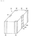
- the noise filter 1 is formed of magnetic layers 2a through 2d, signal lines 3 and 4, ground electrodes 5, a dielectric member 7, signal electrode terminals 8 and 9, and ground electrode terminals 10, which are described below.
- the magnetic layers 2a through 2d form a laminated unit 2 generally formed in the shape of a prism, which serves as an insulating medium to form the outer shape of the noise filter 1.
- the magnetic layers 2a through 2d which serve as insulating layers, are formed by laminating four magnetic sheets and then by pressing and firing them.
- the magnetic layers 2a through 2d are formed generally in the shape of a flat quadrilateral by using a ceramic material (magnetic material) exhibiting magnetic characteristics, for example, ferrite.
- the relative magnetic permeability ⁇ r0 of the magnetic layers 2a through 2d is set to be, for example, about 4 to 1000 (4 ⁇ ⁇ r0 ⁇ 1000), and the relative dielectric constant ⁇ r0 is set to be, for example, about 10.
- a magnetic material be used for the magnetic layers 2a and 2d.
- an insulating resin film may be used for the magnetic layer 2a
- an insulating ceramic substrate for example, an alumina substrate
- the magnetic layer 2a may be omitted.
- the ground electrode 5 formed on the obverse surface of the magnetic layer 2d in Fig. 2 may be formed on the reverse surface of the magnetic layer 2c, thereby also making it possible to omit the magnetic layer 2d.
- the four magnetic layers 2a through 2d may be formed of the same material.
- Fired magnetic layers for example, ferrite plates, may be used for the magnetic layers 2a through 2d.
- bonding layers which are thin enough not to influence the characteristics of the magnetic layers 2a through 2d may be used for coupling them.
- the two signal lines 3 and 4 are disposed between the magnetic layers 2b and 2c.
- the signal lines 3 and 4 extend parallel to each other with a predetermined spacing in such a manner that they extend back and forth along the width of the magnetic layers 2b and 2c in a zigzag manner (meandering) while extending in the longitudinal direction of the magnetic layers 2b and 2c.
- the signal lines 3 and 4 may extend back and forth in the longitudinal direction of the magnetic layers 2b and 2c so as to be extended along the width thereof.
- the signal lines 3 and 4 may be formed generally in a strip-like shape by using a conductive metal material, for example, a silver paste or palladium. Ends 3A of the signal line 3 and ends 4A of the signal line 4 are connected to the signal electrode terminals 8 and 9, respectively, which are described below.
- the signal lines 3 and 4 are positioned substantially at the center of the thickness of the two ground electrodes 5, which are described below, and are substantially entirely covered with the ground electrodes 5 so as to form a transmission line 6.
- the signal lines 3 and 4 have the same width, and the distance between the two ground electrodes 5 is maintained substantially at a constant value along the entire surface of the magnetic layers 2b and 2c. Since the characteristic impedance of the transmission line 6 is substantially determined by the width of the signal lines 3 and 4, the distance between the ground electrodes 5, and the magnetic permeability and the dielectric constant of the magnetic layers 2a and 2b, it is maintained substantially at a constant value along the entire length of the transmission line 6.
- the ground electrodes 5 are formed generally in the shape of a flat quadrilateral by using a conductive metal material, for example, a silver paste or palladium, and cover substantially the entire surface of the magnetic layers 2b and 2c.
- Electrode portions 5A projecting in a tongue-like shape in the widthwise direction (left and right sides in Fig. 2) of the ground electrodes 5 are provided at the intermediate portions of the magnetic layers 2b and 2c in the longitudinal direction (front-to-back direction in Fig. 2).
- the electrode portions 5A are connected to the ground electrode terminals 10, which are described below.
- the ground electrodes 5 form the transmission line 6 together with the magnetic layers 2b and 2c and the signal lines 3 and 4, and are covered with the magnetic layers 2a and 2d.
- the dielectric member 7 is formed of a non-magnetic medium, which is made of a material different from that for the magnetic layers 2b and 2c, and is disposed between the signal lines 3 and 4.
- the relative magnetic permeability ⁇ r1 of the dielectric member 7 is smaller than the relative magnetic permeability ⁇ r0 of the magnetic layers 2b and 2c, and is set to be, for example, about 1 ( ⁇ r1 ⁇ 1).
- the relative dielectric constant ⁇ r1 of the dielectric member 7 is set to be substantially the same as the relative dielectric constant ⁇ r0 of the magnetic layers 2b and 2c.
- the dielectric member 7 fills in the space between the two signal lines 3 and 4.
- the thickness of the dielectric member 7 is substantially the same as the signal lines 3 and 4.
- the present invention is not restricted to such an arrangement, and, for example, in order to obtain a large difference in characteristics between the common mode and the normal mode, the thickness of the dielectric member 7 should be greater than that of the signal lines 3 and 4 to such a degree as not to interfere with an electromagnetic field of the common mode.
- a magnetic member having a relative magnetic permeability lower than the magnetic layers 2b and 2c i.e., a low-magnetic-permeability magnetic member, may be used.
- a gap (space) may be formed between the signal lines 3 and 4 so as to form the member 7.
- the relative dielectric constant ⁇ r1 of the dielectric member 7 be set to be the same as the relative dielectric constant ⁇ r0 of the magnetic layers 2b and 2c; the relative dielectric constant ⁇ r1 may be suitably set so that the characteristic impedance of the normal mode can be a predetermined value.
- the difference of the material characteristics therebetween should be small. Accordingly, as a combination of the member 7 and the insulating medium, glass and ferrite, or ferrite having low magnetic permeability and ferrite having high magnetic permeability may be selected.
- the signal electrode terminals 8 and 9 cover both end portions along the width of the laminated unit 2 and also partially extend to the obverse and reverse surfaces of the laminated unit 2.
- the signal electrode terminals 8 and 9 are formed, for example, by coating the edges of the laminated unit 2 with a conductive metal material and by firing it to plate it.
- the signal electrode terminals 8 and 9 are connected to the electrode portions 3A and 4A of the signal lines 3 and 4, respectively.
- the ground electrode terminals 10 are provided at the center positions in the longitudinal direction of the laminated unit 2, and are formed generally in an angular U shape.
- the ground electrode terminals 10 extend in a strip-like shape on the side surface along the thickness of the laminated unit 2, and partially extend to the obverse and reverse surfaces of the laminated unit 2.
- the ground electrode terminals 10 are formed, for example, by coating the side surfaces of the laminated unit 2 with a conductive metal material and by firing it to plate it.
- the ground electrode terminals 10 are connected to the electrode portions 5A of the ground electrodes 5.
- the noise filter 1 is disposed on a substrate on which two wiring patterns through which differential signals are transmitted are provided.
- the signal electrode terminals 8 are connected to the mid-portion of one wiring pattern, and the signal electrodes 9 are connected to the mid-portion of the other wiring pattern.
- the ground electrode terminals 10 are connected to ground terminals. With this arrangement, signals are transmitted through the transmission line 6 formed by the signal lines 3 and 4 and the ground electrodes 5, and the ground electrodes 5 are maintained at a ground potential.
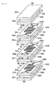
- the directions of the currents supplied to the signal lines 3 and 4 are the same.
- the signal lines 3 and 4 are disposed adjacent to each other, magnetic fluxes generated by the signal lines 3 and 4 are intensified, so that the signal lines 3 and 4 serve as a single line for the common-mode signal.
- the signal lines 3 and 4 are formed between the magnetic layers 2b and 2c. Accordingly, the transmission line 6 formed by the signal lines 3 and 4 and the ground electrodes 5 for the common-mode signal has inductors L, and capacitors C between the signal lines 3 and 4 and the ground electrodes 5 due to the dielectric constant of the magnetic layers 2b and 2c, as indicated by an equivalent circuit shown in Fig. 5.
- the signal lines 3 and 4 serve equivalently as a distributed constant circuit, and a common-mode signal flowing in the signal lines 3 and 4 is transmitted without loss in a frequency range in which the inductors L and the capacitors C are maintained at constant values.
- the frequency of the common-mode signal becomes higher, the magnetic permeability of the magnetic layers 2b and 2c is changed, resulting in the occurrence of loss R (magnetic loss) in the inductors L, as indicated by an equivalent circuit shown in Fig. 6. Accordingly, the common-mode signal in a high frequency range is attenuated due to magnetic loss.
- the effective material characteristic is the same regardless of whether the common mode or the normal mode is employed. That is, the ratio of the loss occurring in the common mode to that in the normal mode does not change over the entire frequency range. If it is desired that the signal be allowed to pass through the filter, the noise suppression effect should be reduced. Conversely, if it is desired that the noise suppression effect be enhanced, the attenuation of the signal is increased.
- the dielectric member 7 having the constant magnetic permeability ⁇ r1, which is smaller than the constant magnetic permeability ⁇ r0 of the magnetic layers 2b and 2c, is disposed between the signal lines 3 and 4. Accordingly, magnetic fluxes ⁇ n generated in the normal mode pass through (transverse) the dielectric member 7, as shown in Fig. 3. In contrast, a magnetic flux ⁇ c generated in the common mode does not pass through the dielectric member 7, as shown in Fig. 4. Accordingly, in the path of the magnetic fluxes ⁇ n generated in the normal mode, the effective relative magnetic permeability ⁇ wn becomes lower by providing the dielectric member 7. Conversely, in the path of the magnetic flux ⁇ c generated in the common mode, the effective relative magnetic permeability ⁇ wc is not decreased.
- the dielectric member 7 is located at a position where only an electromagnetic field substantially generated by normal-mode signal is present, and an electromagnetic field substantially generated by common-mode signal is not present.
- the frequency corresponding to the loss peak (frequency at which the real part ⁇ ' and the imaginary part ⁇ " of the effective relative magnetic permeability become the same) is shifted to a higher range. Accordingly, without the dielectric member 7, the loss peak appears at several megahertz, as shown in Fig. 8. In contrast, with the dielectric member 7, the loss peak appears at several tens of megahertz, as shown in Fig. 9.
- the magnitude of the loss itself determined by the ratio of the imaginary part ⁇ " to the real part ⁇ ' ( ⁇ "/ ⁇ ') of the magnetic permeability and the magnitude of the real part ⁇ ' becomes smaller than that without the dielectric member 7.
- the normal-mode signal can propagate without being attenuated up to the high frequency range, while the common-mode signal can be removed in the low frequency range. Therefore, the normal-mode signal, which is a required mode, can be transmitted without causing blunt waves. Accordingly, the noise suppression effect can be enhanced while maintaining the waveform quality.
- the characteristic impedance of each of the signal lines 3 and 4 can be set.
- the characteristic impedance of the normal mode can be set.
- the above-described characteristic impedances can be maintained substantially at constant values. Accordingly, by setting the material characteristics so that the signal frequency is contained within the above-described frequency range, impedance matching to a circuit connected to the noise filter 1 can be provided. Thus, the reflection loss of the noise filter 1 can be reduced, thereby suppressing the noise caused by resonance and the distortion of the signal waveform.
- the signal lines 3 and 4 are disposed between the two magnetic layers 2b and 2c, and the magnetic layers 2b and 2c are sandwiched by the two ground electrodes 5.
- the transmission line 6 can be formed by covering the entire lengths of the signal lines 3 and 4 positioned between the magnetic layers 2b and 2c with the two ground electrodes 5. Accordingly, the common-mode characteristic impedance can be set to a constant value over the entire length of the transmission line 6, thereby preventing noise from being reflected in the transmission line 6 and preventing noise resonance. Since the entire lengths of the signal lines 3 and 4 are covered with the two ground electrodes 5, noise can be prevented from entering the signal lines 3 and 4 from the exterior, thereby enhancing the transmission reliability of the signal.
- the normal-mode characteristic impedance and the common-mode characteristic impedance of the transmission line 6 can be individually set. Accordingly, for the common-mode characteristic impedance associated with common-mode noise, impedance matching to an external circuit to be connected to the noise filter 1 may be provided or impedance matching to the external circuit may not be provided while providing normal-mode characteristic impedance matching for the external circuit.
- common-mode characteristic impedance matching is not provided, noise can be suppressed by utilizing the reflection loss.
- common-mode characteristic impedance matching is not provided, noise can be suppressed by utilizing thermal loss in the magnetic layers 2b and 2c while preventing problems, for example, resonance, caused by the reflection.
- the common-mode characteristic impedance can be set independently of the normal-mode characteristic impedance.
- the transmission loss for the common-mode signal can be increased by utilizing the reflection loss and/or thermal loss compared to that of the related art.
- the noise filter 1 when the frequency of common-mode noise is low, the noise filter 1 allows the common-mode noise to pass therethrough, and thus, it serves as a lowpass filter. That is, the noise filter 1 has a pass band and an attenuation band for the common-mode noise according to the frequency.
- the pass band and the attenuation band can be determined by adjusting the composition (relative magnetic permeability) of the magnetic material for the magnetic layers 2b and 2c and the lengths of the signal lines 3 and 4.
- the composition of the material for the magnetic layers 2b and 2c and the lengths of the signal lines 3 and 4 are set so that the common-mode noise can be reliably attenuated.
- the signal lines 3 and 4 are disposed between the two magnetic layers 2b and 2c, and the magnetic layers 2b and 2c are covered with the two ground electrodes 5.
- the magnetic loss thermal loss
- the dielectric member 7 the effective relative magnetic permeability is decreased so that it can be maintained at a constant value up to the high frequency range.
- the normal-mode characteristic impedance of the signal lines 3 and 4 can be maintained substantially at a constant value in a wide frequency range, thereby facilitating the provision of impedance matching to an external circuit.
- the reflection loss of the noise filter 1 can be reduced, thereby preventing the noise from being intensified as a result of resonance and preventing distortion of the signal waveform.
- the frequency characteristic of the effective relative magnetic permeability ⁇ wn with respect to the normal-mode signal can be changed without influencing the common-mode signal, thereby shifting the frequency at which the magnetic loss R peaks to a higher frequency range. Accordingly, the common-mode signal can be eliminated at lower frequencies, and the normal-mode signal can be transmitted without being attenuated up to the high frequency range. As a result, the quality of waveforms can be maintained for the normal-mode signal by preventing blunt waves without decreasing the noise suppression effect for the common-mode signal.
- the signal lines 3 and 4 positioned between the magnetic layers 2b and 2c are entirely covered with the two ground electrodes 5. Accordingly, the common-mode characteristic impedance can be set to a constant value over the entire length of the transmission line 6 formed by the signal lines 3 and 4 and the ground electrodes 5. As a result, noise can be prevented from being reflected in the transmission line 6 and can also be prevented from entering the transmission line 6 from the exterior, thereby allowing the signal to be reliably transmitted.
- the normal-mode characteristic impedance and the common-mode characteristic impedance of the transmission line 6 can be individually set. Accordingly, for the common-mode characteristic impedance associated with common-mode noise, impedance matching to an external circuit may be provided or impedance matching to the external circuit may not be provided while providing normal-mode impedance matching to the external circuit. Regardless of whether or not common-mode impedance matching is provided, the transmission loss for the common-mode signal can be increased by using the reflection loss and/or thermal loss compared to the related art.
- the magnetic layers 2a through 2d are formed generally in the shape of a quadrilateral, and the signal electrode terminals 8 and 9 respectively connected to the ends 3A and 4A of the signal lines 3 and 4 are provided at both ends in the longitudinal direction of the magnetic layers 2a through 2d.
- the ground electrode terminals 10 connected to the ground terminals 5 are disposed at the intermediate portions in the longitudinal direction of the magnetic layers 2a through 2d. With this configuration, the signal electrode terminals 8 and 9 can be easily connected to the mid-portions of longitudinally extending wiring patterns.
- the ground electrode terminals 10 can also be easily connected to ground terminals, which are disposed around the wiring patterns. It is thus possible to facilitate the assembly of the noise filter 1.
- the signal lines 3 and 4 are formed in a zigzag manner (meandering), the lengths of the signal lines 3 and 4 can be increased, thereby increasing the attenuation of noise.
- signal lines 3 and 4 are formed in a zigzag manner, signal lines 3' and 4' may be formed in a coil-like shape, as in a first modified example shown in Fig. 10.
- a noise filter 11 constructed in accordance with a second embodiment of the present invention is described below with reference to Figs. 11 through 14.
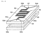
- the features of the noise filter 11 of the second embodiment are as follows. Two signal lines are disposed side by side on the obverse surface of a magnetic layer, and a ground electrode is disposed on the reverse surface of the magnetic layer. A dielectric member is provided between the two signal lines, and the two signal lines are coated with a coating film exhibiting magnetic characteristics.
- the noise filter 11 is formed of magnetic layers 12a and 12b, signal lines 13 and 14, a ground electrode 15, a dielectric member 17, a coating film 18, signal electrode terminals 19 and 20, and ground electrode terminals 21, which are described below.
- a laminated unit 12 is generally formed in the shape of a prism, which serves as an insulating medium to form the outer shape of the noise filter 1.
- the laminated unit 12 is formed by firing the magnetic layers 12a and 12b.
- the magnetic layers 12a and 12b are formed generally in the shape of a flat quadrilateral (rectangle) by using, for example, ferrite.
- the signal lines 13 and 14 which are disposed on the obverse surface of the magnetic layer 12a, extend parallel to each other with a predetermined spacing therebetween while extending in the longitudinal direction of the magnetic layer 12a in a zigzag manner.
- the signal lines 13 and 14 are formed generally in a strip-like shape by using a conductive metal material.
- the reverse sides of the signal lines 13 and 14 are substantially entirely covered with the ground electrode 15, which is described below, so as to form a transmission line 16.
- the signal lines 13 and 14 form electrode portions 13A and 14A, respectively, at the ends thereof so as to be connected to the signal electrode terminals 19 and 20, respectively.
- the ground electrode 15 which is disposed on the reverse surface of the magnetic layer 12a (between the magnetic layers 12a and 12b), is formed generally in the shape of a flat quadrilateral by using a conductive metal material, and covers the almost entire reverse surface of the magnetic layer 12a. Electrode portions 15A projecting in a tongue-like shape in the widthwise direction of the ground electrode 15 are provided at the intermediate portions in the longitudinal direction of the magnetic layer 12a, and are connected to the ground electrode terminals 21, which are described below. The ground electrode 15 forms the transmission line 16 together with the magnetic layer 12a and the two signal lines 13 and 14.
- the dielectric member 17 is a medium disposed between the signal lines 13 and 14, and is formed of a material similar to that for the dielectric member 7 of the first embodiment.
- the relative magnetic permeability ⁇ r1 of the dielectric member 17 is smaller than the relative magnetic permeability ⁇ r0 of the magnetic layer 12a, and is set to be, for example, about 1 ( ⁇ r1 ⁇ 1).
- the relative dielectric constant ⁇ r1 of the dielectric member 17 is set to be substantially the same as the relative dielectric constant ⁇ r0 of the magnetic layer 12a.
- the dielectric member 17 fills in the space between the two signal lines 13 and 14.
- the coating film 18, which is disposed on the obverse surface of the laminated unit 12, is formed by mixing magnetic powder with a resin material.
- the coating film 18 has a relative magnetic permeability ⁇ r2, which is almost the same as the magnetic permeability ⁇ r0 of the magnetic layer 12a and is higher than the relative magnetic permeability ⁇ r1 of the dielectric member 17.
- the coating film 18 then covers the two signal lines 13 and 14 including the dielectric member 17.
- the signal electrode terminals 19 and 20, which are provided at the four corners of the laminated unit 12, are formed generally in an angular U-shape by using a conductive metal material, as in the first embodiment, and are connected to the electrode portions 13A and 14A of the signal lines 13 and 14, respectively.
- the ground electrode terminals 21, which are provided on both side surfaces in the widthwise direction and at the intermediate portions in the longitudinal direction of the laminated unit 12, and are formed generally in an angular U-shape by using a conductive metal material, as in the first embodiment, and are connected to the electrode portions 15A of the ground electrode 15.
- the dielectric member 17 is disposed between the two signal lines 13 and 14. Additionally, in the second embodiment, the signal lines 13 and 14 and the dielectric member 17 are coated with the coating film 18. Accordingly, as shown in Figs. 13 and 14, both in the normal mode and the common mode, magnetic fluxes ⁇ n and ⁇ c can be trapped in the coating film 18 and the magnetic layer 12a, and also, the effective relative magnetic permeability ⁇ wn of the normal mode can be decreased without influencing the effective relative magnetic permeability ⁇ wc of the common mode. Thus, advantages similar to those achieved by the first embodiment can be obtained.
- Figs. 15 and 16 illustrate a noise filter 31 constructed in accordance with a third embodiment of the present invention.
- the features of the noise filter 31 of the third embodiment are as follows.
- a plurality of magnetic layers overlaid on each other, first and second signal lines disposed side by side with a gap therebetween between the magnetic layers, and two ground electrodes disposed on the top surface and the bottom surface across the magnetic layers including the two signal lines form a transmission line.
- a plurality of (for example, two) layers of such transmission lines are laminated so that the first signal lines are connected in series with each other and the second signal lines are connected in series with each other between the transmission line layers, and a dielectric member is disposed between the first and second signal lines of each transmission line layer.
- the noise filter 31 is formed of magnetic layers 32a through 32h, first signal lines 33, 35, and 37, second signal lines 34, 36, and 38, ground electrodes 39, dielectric members 41, first and second signal electrode terminals 42 and 43, and ground electrode terminals 44, which are described below.
- a laminated unit 32 which is generally formed in the shape of a prism so as to form the outer shape of the noise filter 31, is formed by laminating the eight magnetic layers 32a through 32h.
- the magnetic layers 32a through 32h are formed generally in the shape of a flat quadrilateral by using a ceramics material exhibiting magnetic characteristics, for example, ferrite, as in the magnetic layers 2a through 2h of the first embodiment.
- the first and second signal lines 33 and 34 which are provided between the magnetic layers 32b and 32c, are disposed parallel to each other with a predetermined spacing therebetween in a zigzag manner by using a conductive metal material, as in the signal lines 3 and 4 of the first embodiment.
- the signal lines 33 and 34 are covered with the two ground electrodes 39 disposed on the top surface of the magnetic layer 32b and the bottom surface of the magnetic layer 32c, thereby forming a first-layer transmission line 40A, which is described below.
- first signal line 33 forms an electrode portion 33A extending toward one end in the longitudinal direction of the laminated unit 32
- second signal line 34 forms an electrode portion 34A toward the same end in the longitudinal direction of the laminated unit 32.
- the other ends of the first and second signal lines 33 and 34 are provided with through-holes 33B and 34B, respectively, away from the other ends in the longitudinal direction of the laminated unit 32 and passing through the magnetic layers 32c and 32d.
- a conductive material fills in the through-holes 33B and 34B, and the first and second signal lines 33 and 34 are connected in series with the first and second signal lines 35 and 36, respectively.
- the first and second signal lines 35 and 36 which are provided between the magnetic layers 32d and 32e, extend parallel to each other with a predetermined spacing therebetween in a zigzag manner by using a conductive metal material, as in the first and second signal lines 3 and 4 of the first embodiment.
- the first and second signal lines 35 and 36 are covered with the two ground layers 39 provided on the top surface of the magnetic layer 32d and the bottom surface of the magnetic layer 32e, thereby forming a second-layer transmission line 40B, which is described below.
- One end of the first signal line 35 forms a connecting portion 35A extending toward one end in the longitudinal direction of the laminated unit 32 and disposed at a position facing the through-hole 33B of the first signal line 33 so that the connecting portion 35A is connected to the first signal line 33.
- One end of the second signal line 36 forms a connecting portion 36A extending toward the same end in the longitudinal direction of the laminated unit 32 and disposed at a position facing the through-hole 34B so that the connecting portion 36A is connected to the second signal line 34.
- the other ends of the first and second signal lines 35 and 36 are respectively provided with through-holes 35B and 36B away from the other end in the longitudinal direction of the laminated unit 32 and passing through the magnetic layers 32e and 32f.
- a conductive material fills in the through-holes 35B and 36B, and the first and second signal lines 35 and 36 are respectively connected to the first and second signal lines 37 and 38, which are described below.
- the first and second signal lines 37 and 38 which are provided between the magnetic layers 32f and 32g, extended parallel to each other with a predetermined spacing therebetween in a zigzag manner by using a conductive metal material, as in the first and second signal lines 3 and 4 of the first embodiment.
- the first and second signal lines 37 and 38 are covered with the two ground layers 39 provided on the top surface of the magnetic layer 32f and the bottom surface of the magnetic layer 32g, thereby forming a third-layer transmission line 40C, which is described below.
- One end of the first signal line 37 forms a connecting portion 37A extending toward one end in the longitudinal direction of the laminated unit 32 and disposed at a position facing the through-hole 35B of the first signal line 35 so that the connecting portion 37A is connected to the first signal line 35.
- One end of the second signal line 38 forms a connecting portion 38A extending toward the same end in the longitudinal direction of the laminated unit 32 and disposed at a position facing the through-hole 36B so that the connecting portion 38A is connected to the second signal line 36.
- the other ends of the first and second signal lines 37 and 38 are respectively provided with electrode portions 37B and 38B extending toward the other end in the longitudinal direction of the laminated unit 32.
- the widths of the signal lines 33 through 38 are set to be substantially the same, and the thickness dimensions of the magnetic layers 32b through 32g are set to be substantially the same.
- the characteristic impedances of the first-, second-, and third-layer transmission lines 40A, 40B, and 40C are substantially equal to each other and are also substantially uniform over the entire lengths thereof.
- the four ground electrodes 39 are provided between the corresponding pairs of magnetic layers 32a and 32b, 32c and 32d, 32e and 32f, and 32g and 32h such that they sandwich the corresponding first and second signal lines 33 through 38 therebetween.
- the ground electrodes 39 are disposed on the top surfaces of the magnetic layers 32b, 32d, 32f, and 32h and on the bottom surfaces of the magnetic layers 32a, 32c, 32e, and 32g.
- the ground electrodes 39 and the signal lines 33 through 38 are alternately laminated. Accordingly, two ground electrodes 39 sandwiching the magnetic layers 32b and 32c including the first and second signal lines 33 and 34 therebetween form the first-layer transmission line 40A.
- the ground electrodes 39 are formed generally in the shape of a flat quadrilateral by using a conductive metal material, and cover substantially the entire surfaces of the magnetic layers 32b through 32g. Electrode portions 39A projecting in a tongue-like shape in the widthwise direction of the ground electrode 39 are provided, as in the ground electrodes 5 of the first embodiment, and are connected to the ground electrode terminals 44, which are described below.
- a dielectric member 41 is provided each between the first and second signal lines 33 and 34, between the first and second signal lines 35 and 36, and between the first and second signal lines 37 and 38.
- the dielectric member 41 is formed by using a material similar to that for the dielectric member 7 of the first embodiment.
- the relative magnetic permeability ⁇ r1 of the dielectric member 41 is smaller than the relative magnetic permeability ⁇ r0 of the magnetic layers 32b through 32g, and is set to be, for example, about 1 ( ⁇ r1 ⁇ 1).
- the relative dielectric constant ⁇ r1 of the dielectric member 41 is set to be substantially the same as the relative dielectric constant ⁇ r0 of the magnetic layers 32b through 32g.
- the dielectric member 41 fills in the space each between the two signal lines 33 and 34, between the two signal lines 35 and 36, and the two signal lines 37 and 38.
- the signal electrode terminals 42 and 43 which are provided at the four corners of the laminated unit 32, are formed generally in an angular U-shape by using a conductive metal material, as in the first embodiment.
- the signal electrode terminals 42 and 43 disposed at one end in the longitudinal direction of the laminated unit 32 are respectively connected to the electrode portions 33A and 34A of the first and second signal lines 33 and 34.
- the signal electrode terminals 42 and 43 disposed at the other end of the laminated unit 32 are respectively connected to the electrode portions 37A and 37B of the first and second signal lines 37 and 38.
- the ground electrode terminals 44 which are provided on side surfaces in the widthwise direction and at the intermediate portions in the longitudinal direction of the laminated unit 32, are formed generally in an angular U-shape by using a conductive metal material, as in the first embodiment, and are connected to the electrode portions 39A of the ground electrode 39.
- the first signal lines 33, 35, and 37 are connected in series with each other, and the second signal lines 34, 36, and 38 are connected in series with each other. Accordingly, the entire length of the first signal lines and the entire length of the second signal lines can be increased, thereby making it possible to increase the attenuation of noise.
- first and second signal lines are formed in a coil-like shape, and the length of the signal line positioned at the inner periphery becomes shorter than the length of the signal line positioned at the outer periphery. Accordingly, it is desired that the positions of the first and second signal lines be changed alternately in the layers so that the entire length of the first signal lines can be the same as that of the second signal lines.
- Figs. 17 through 20 illustrate a noise filter 51 constructed in accordance with a fourth embodiment of the present invention.
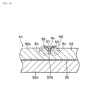
- the features of the noise filter 51 of this embodiment are as follows. Two signal lines are disposed side by side on the obverse surface of a dielectric layer, and a ground electrode is disposed on the reverse surface of the dielectric layer. An incision groove is provided between the two signal lines.
- the noise filter 51 is formed of dielectric layers 52a and 52b, signal lines 53 and 54, a ground electrode 55, an incision groove 57, signal electrode terminals 58 and 59, and ground electrode terminals 60, which are described below.
- a laminated unit 52 which is generally formed in the shape of a prism so as to form the outer shape of the noise filter 51, is formed by firing the dielectric layers 52a and 52b.
- the dielectric layers 52a and 52b are formed generally in the shape of a flat quadrilateral by using a dielectric material, such as a ceramic material.
- the relative dielectric constant ⁇ r2 of the dielectric layers 52a and 52b is greater than 1 ( ⁇ r2 > 1), and the relative magnetic permeability ⁇ r2 thereof is set to be about 1 ( ⁇ r2 ⁇ 1) .
- the two signal lines 53 and 54 which are disposed on the obverse surface of the dielectric layer 52a, extend parallel to each other with a predetermined spacing therebetween in the longitudinal direction of the dielectric layer 52a in a zigzag manner.
- the signal lines 53 and 54 are formed generally in a strip-like shape by using a conductive metal material, as in the first embodiment, and the reverse side of the signal lines 53 and 54 are substantially entirely covered with the ground electrode 55, which is described below, thereby forming a transmission line 56.
- the signal lines 53 and 54 form electrode portions 53A and 54A at both ends, and are respectively connected to the signal electrode terminals 58 and 59, which are described below.
- the ground electrode 55 which is provided on the reverse surface of the dielectric layer 52a (between the dielectric layers 52a and 52b), is formed generally in the shape of a quadrilateral by using a conductive metal material, and covers substantially the entire surface of the dielectric layer 52a. Electrode portions 55A projecting in a tongue-like shape in the widthwise direction of the ground electrode 55 are provided at the intermediate portions of the magnetic layer 52a in the longitudinal direction, and are connected to the ground electrode terminals 60, which are described below. The ground electrode 55 forms the transmission line 56 together with the dielectric layer 52a and the two signal lines 53 and 54.
- the incision groove 57 which is formed between the two signal lines 53 and 54 on the obverse surface of the dielectric layer 52a, is formed in a zigzag manner along the signal lines 53 and 54.
- the incision groove 57 is positioned substantially at the center between the signal lines 53 and 54 and has a predetermined depth toward the ground electrode 55.
- the depth of the incision groove 57 is set so that an electric flux Dn of the normal mode passes through the incision groove 57 and so that an electric flux Dc does not pass through the incision groove 57.
- a space 57A having a relative dielectric constant ⁇ r3 of about 1 and a relative magnetic permeability ⁇ r3 of about 1 is defined.
- the signal electrode terminals 58 and 59 which are provided at the four corners of the laminated unit 52, are formed generally in an angular U-shape by using a conductive metal material, as in the first embodiment, and are respectively connected to the electrode portions 53A and 54A of the signal lines 53 and 54.
- the ground electrode terminals 60 which are provided on both side surfaces in the widthwise direction and at the intermediate portions in the longitudinal direction of the laminated unit 52, are formed generally in an angular U-shape by using a conductive metal material, as in the first embodiment, and are connected to the electrode portions 55A of the ground electrode 55.
- the two signal lines 53 and 54 are disposed side by side on the obverse surface of the dielectric layer 52a, and the ground electrode 55 is provided on the reverse surface of the dielectric layer 52a.
- dielectric loss thermal loss
- the transmission line 56 is formed by covering the entire reverse side of the signal lines 53 and 54 with the ground electrode 55, the characteristic impedance can be set to a constant value over the entire transmission line 56. Accordingly, impedance matching to an external circuit can be easily provided. It is also possible to prevent noise from being reflected in the transmission line 60 and from being intensified as a result of resonance.
- the electric flux Dn generated in the normal mode passes through the space 57A in the incision groove 57, as shown in Fig. 19, while the electric flux Dc generated in the common mode does not pass through the space 57A, as shown in Fig. 20. Accordingly, by utilizing the space 57A, the effective relative dielectric constant of the normal mode ⁇ wn can be decreased without influencing the effective relative dielectric constant ⁇ wc of the common mode. Thus, as in the first embodiment, only the normal-mode loss can be reduced, thereby enhancing the noise suppression effect without distorting the signal waveform.
- the obverse surface of the dielectric layer 52a is exposed.
- it may be coated with, for example, a resin material having a relative dielectric constant lower than the relative dielectric constant ⁇ r2 of the dielectric layer 52a.
- Figs. 21 through 23 illustrate a noise filter 61 constructed in accordance with a fifth embodiment of the present invention.
- the features of the noise filter 61 of the fifth embodiment are as follows. Three overlaid magnetic layers are provided, and two signal lines are disposed side by side across the intermediate magnetic layer. A ground electrode is provided on the top surface of the uppermost layer and on the bottom surface of the lowermost layer, thereby forming a transmission line.
- the noise filter 61 is formed of magnetic layers 62a through 62c, signal lines 63 and 64, ground electrodes 65, a dielectric member 67, signal electrode terminals 68 and 69, and ground electrode terminals 70, which are described below.
- a laminated unit 62 which is formed generally in the shape of a prism so as to form the outer shape of the noise filter 61, is formed by the three magnetic layers 62a through 62c.
- the upper and lower magnetic layers 62a and 62c are formed by, for example, ferrite, and the intermediate magnetic layer 62b is formed by, for example, a magnetic composite material generated by kneading ferrite powder into polyimide.
- the magnetic layers 62a through 62c are generally formed in the shape of a flat quadrilateral (rectangle).
- the two signal lines 63 and 64 which are disposed on the obverse surface and the reverse surface, respectively, of the intermediate magnetic layer 62b, face each other across the intermediate magnetic layer 62b and extend parallel to each other with a predetermined spacing therebetween in the longitudinal direction of the magnetic layer 62b in a zigzag manner.
- the signal lines 63 and 64 are formed in a strip-like shape by using a conductive metal material, as in the first embodiment, and are substantially entirely covered with the ground electrodes 65, which are described below, thereby forming a transmission line 66.
- the signal lines 63 and 64 form electrode portions 63A and 64A, respectively, at both ends, which are connected to the signal electrode terminals 68 and 69, respectively, which are described below.
- Widths W1 and W2 of the signal lines 63 and 64 may be set to be the same value or different values.
- the width W2 of the signal line 64 positioned on the reverse surface of the magnetic layer 62b may be set to be greater than the width W1 of the signal line 63 positioned on the obverse surface of the magnetic layer 62b.
- the two ground electrodes 65 which are disposed on the obverse surface of the magnetic layer 62a and the reverse surface of the magnetic layer 62c, sandwich the laminated unit 62 from the top and the bottom.
- the ground electrodes 65 are formed generally in the shape of a flat quadrilateral by using a conductive metal material, and cover substantially the entire surfaces of the magnetic layers 62a and 62c.
- Electrode portions 65A projecting in a tongue-like shape in the widthwise direction of the ground electrodes 65 are provided at the intermediate portions in the longitudinal direction of the magnetic layers 62a and 62c, and are connected to the ground electrode terminals 70, which are described below.
- the ground electrodes 65 form the transmission line 66 together with the magnetic layers 62a through 62c and the two signal lines 63 and 64.
- the dielectric member 67 which is a medium made of a material different from a magnetic medium, for example, polyimide, is disposed between the signal lines 63 and 64.
- the relative magnetic permeability ⁇ r1 of the dielectric member 67 is smaller than the relative magnetic permeability ⁇ r0 of the magnetic layers 62a through 62c, and is set to be, for example, about 1 ( ⁇ r1 ⁇ 1).
- the relative dielectric constant ⁇ r1 of the dielectric member 67 is set to be substantially the same as the relative dielectric constant ⁇ r0 of the magnetic layers 62a through 62c.
- the dielectric member 67 is formed in the magnetic layer 62b in a zigzag manner along the two signal lines 63 and 64.
- the width W3 of the dielectric member 67 may be set to be the substantially same as the widths W1 and W2 of the signal lines 63 and 64. Alternatively, by considering the processing precision, the width W3 may be set to be greater than the widths W1 and W2.
- the signal electrode terminals 68 and 69 which are provided at the four corners of the laminated unit 62, are formed by using a conductive metal material, as in the first embodiment, and are connected to the electrode portions 63A and 64A of the signal lines 63 and 64, respectively.
- the ground electrode terminals 70 which are provided at both side surfaces in the widthwise direction and at the intermediate portions in the longitudinal direction of the laminated unit 62, are formed generally in an angular U-shape by using a conductive metal material, as in the first embodiment, and are connected to the electrode portions 65A of the ground electrode 65.
- the signal lines 3, 4, 13, 14, 33 through 38, 53, 54, 63, and 64 are formed in a zigzag manner or in a coil-like shape.
- the present invention is not restricted to this arrangement, and, for example, linear signal lines may be formed.
- the dielectric member 7 which is a medium made of a material different from a magnetic medium, is disposed between two signal lines (for example, signal lines 3 and 4).
- the present invention is not limited to this arrangement.
- the dielectric member 7 may be positioned in the presence of only one of an electromagnetic field substantially generated by the common-mode signal and an electromagnetic field substantially generated by the normal-mode signal.
- a medium 71 may be disposed in the thickness direction while extending from the signal lines 3 and 4 upward and downward by being separated from each other.
- the magnetic flux ⁇ c in the common mode passes through the medium 71, while the magnetic fluxes ⁇ n in the normal mode do not pass through the medium 71.
- a magnetic material having a relative magnetic permeability higher than that of the magnetic layers 2b and 2c can be selected for the medium 71, thereby making it possible to increase the loss of the common-mode signal without influencing the normal-mode signal.
- the dielectric members 17 and 41 formed of a non-magnetic medium are used.
- a low-magnetic-permeability material or a space may be used.
- two signal lines are positioned in the same layer and are horizontally separated.
- two signal lines 3" and 4" may be positioned in different layers in a laminated unit 2" and may be separated from each other in the thickness direction.
- a magnetic layer 81 which is formed of a magnetic material similar to magnetic layers 2b" and 2c" is disposed between the magnetic layers 2b" and 2c", and a medium made of a material different from the magnetic layers 2b" and 2c", for example, a dielectric member 82 is disposed between the signal line 3" and 4".
Landscapes
- Physics & Mathematics (AREA)
- Electromagnetism (AREA)
- Filters And Equalizers (AREA)
- Coils Or Transformers For Communication (AREA)
Applications Claiming Priority (4)
| Application Number | Priority Date | Filing Date | Title |
|---|---|---|---|
| JP2002240906 | 2002-08-21 | ||
| JP2002240906 | 2002-08-21 | ||
| JP2003201298 | 2003-07-24 | ||
| JP2003201298A JP4370838B2 (ja) | 2002-08-21 | 2003-07-24 | ノイズフィルタ |
Publications (2)
| Publication Number | Publication Date |
|---|---|
| EP1432136A2 true EP1432136A2 (de) | 2004-06-23 |
| EP1432136A3 EP1432136A3 (de) | 2005-03-16 |
Family
ID=32072432
Family Applications (1)
| Application Number | Title | Priority Date | Filing Date |
|---|---|---|---|
| EP03255174A Withdrawn EP1432136A3 (de) | 2002-08-21 | 2003-08-21 | Rauschfilter |
Country Status (5)
| Country | Link |
|---|---|
| US (1) | US6853268B2 (de) |
| EP (1) | EP1432136A3 (de) |
| JP (1) | JP4370838B2 (de) |
| KR (1) | KR100568506B1 (de) |
| CN (1) | CN1259673C (de) |
Families Citing this family (30)
| Publication number | Priority date | Publication date | Assignee | Title |
|---|---|---|---|---|
| KR100635699B1 (ko) * | 2002-07-31 | 2006-10-17 | 엔이씨 도낀 가부시끼가이샤 | 큰 직류 하에서도 발열이 적은 전송선로형 노이즈 필터 |
| US6956444B2 (en) * | 2003-02-14 | 2005-10-18 | Intel Corporation | Method and apparatus for rejecting common mode signals on a printed circuit board and method for making same |
| JP2004343084A (ja) * | 2003-04-21 | 2004-12-02 | Murata Mfg Co Ltd | 電子部品 |
| JP2006179596A (ja) * | 2004-12-21 | 2006-07-06 | Mitsubishi Electric Corp | 半導体装置 |
| JP2006332302A (ja) * | 2005-05-26 | 2006-12-07 | Murata Mfg Co Ltd | コモンモードチョークコイル実装基板及びコモンモードチョークコイル実装方法 |
| KR100723531B1 (ko) * | 2006-06-13 | 2007-05-30 | 삼성전자주식회사 | 반도체 패키지 기판 |
| JP5045058B2 (ja) * | 2006-10-25 | 2012-10-10 | パナソニック株式会社 | π型フィルタ |
| US7538653B2 (en) * | 2007-03-30 | 2009-05-26 | Intel Corporation | Grounding of magnetic cores |
| DE102008019127B4 (de) * | 2008-04-16 | 2010-12-09 | Epcos Ag | Vielschichtbauelement |
| DE102008035102A1 (de) * | 2008-07-28 | 2010-02-11 | Epcos Ag | Vielschichtbauelement |
| CN102349189B (zh) * | 2009-03-18 | 2014-10-29 | 株式会社村田制作所 | 电子元器件 |
| EP2520216B1 (de) * | 2010-07-30 | 2014-02-26 | Olympus Medical Systems Corp. | Endoskopsystem |
| KR200454349Y1 (ko) * | 2011-01-12 | 2011-06-29 | (주)우리조경건설 | 목재 마감재가 구비된 파고라 기둥 |
| CN102790599B (zh) * | 2012-07-30 | 2015-09-09 | 华为技术有限公司 | 滤波器 |
| JP5660258B2 (ja) * | 2012-08-24 | 2015-01-28 | 株式会社村田製作所 | 高周波デバイス及び方向性結合器 |
| US9324490B2 (en) | 2013-05-28 | 2016-04-26 | Tdk Corporation | Apparatus and methods for vector inductors |
| US9570222B2 (en) | 2013-05-28 | 2017-02-14 | Tdk Corporation | Vector inductor having multiple mutually coupled metalization layers providing high quality factor |
| KR101983151B1 (ko) * | 2013-10-15 | 2019-05-28 | 삼성전기주식회사 | 공통 모드 필터 |
| US9906203B2 (en) * | 2013-11-26 | 2018-02-27 | Samsung Electro-Mechanics Co., Ltd. | Common mode filter and electronic device including the same |
| KR101973412B1 (ko) * | 2013-12-31 | 2019-09-02 | 삼성전기주식회사 | 공통 모드 필터 |
| CN104966601A (zh) * | 2014-03-26 | 2015-10-07 | 莱尔德电子材料(深圳)有限公司 | 用于共模扼流圈的非磁性铁氧体电介质 |
| US9735752B2 (en) | 2014-12-03 | 2017-08-15 | Tdk Corporation | Apparatus and methods for tunable filters |
| JP6414529B2 (ja) * | 2015-09-25 | 2018-10-31 | 株式会社村田製作所 | 電子部品 |
| JP6565555B2 (ja) * | 2015-09-30 | 2019-08-28 | Tdk株式会社 | 積層コモンモードフィルタ |
| KR101735599B1 (ko) * | 2015-11-11 | 2017-05-16 | 주식회사 모다이노칩 | 회로 보호 소자 |
| JP6614109B2 (ja) * | 2016-11-21 | 2019-12-04 | 株式会社村田製作所 | 無線回路搭載電子機器 |
| JP6845540B2 (ja) * | 2017-05-17 | 2021-03-17 | 国立大学法人信州大学 | 単層薄膜コモンモードフィルタ |
| JP6696483B2 (ja) * | 2017-07-10 | 2020-05-20 | 株式会社村田製作所 | コイル部品 |
| KR102105385B1 (ko) * | 2018-07-18 | 2020-04-28 | 삼성전기주식회사 | 코일 부품 |
| CN112909455B (zh) * | 2019-11-19 | 2022-04-05 | 英业达科技有限公司 | 噪声抑制滤波器及制作噪声抑制滤波器的方法 |
Citations (2)
| Publication number | Priority date | Publication date | Assignee | Title |
|---|---|---|---|---|
| JP3215917B2 (ja) | 1990-05-18 | 2001-10-09 | ザ ダウ ケミカル カンパニー | ポリオレフィン積層粘着性フィルム |
| WO2002056322A1 (en) | 2001-01-15 | 2002-07-18 | Matsushita Electric Industrial Co., Ltd. | Noise filter and electronic apparatus comprising this noise filter |
Family Cites Families (5)
| Publication number | Priority date | Publication date | Assignee | Title |
|---|---|---|---|---|
| FR2077965B1 (de) * | 1970-02-27 | 1973-11-16 | Anvar | |
| JP2959787B2 (ja) * | 1990-01-20 | 1999-10-06 | 毅 池田 | 積層型lcノイズフィルタ及びその製造方法 |
| JP3089666B2 (ja) * | 1993-08-27 | 2000-09-18 | 株式会社村田製作所 | 高周波伝送線路、高周波共振器、高周波フィルタ及び高周波帯域除去フィルタ |
| JP3252605B2 (ja) * | 1994-07-04 | 2002-02-04 | 株式会社村田製作所 | 電子部品及びその製造方法 |
| US6806794B2 (en) * | 2000-08-12 | 2004-10-19 | Murata Manufacturing Co., Ltd. | Noise filter |
-
2003
- 2003-07-24 JP JP2003201298A patent/JP4370838B2/ja not_active Expired - Fee Related
- 2003-08-20 CN CNB031548482A patent/CN1259673C/zh not_active Expired - Fee Related
- 2003-08-21 EP EP03255174A patent/EP1432136A3/de not_active Withdrawn
- 2003-08-21 US US10/644,780 patent/US6853268B2/en not_active Expired - Lifetime
- 2003-08-21 KR KR1020030057961A patent/KR100568506B1/ko not_active Expired - Fee Related
Patent Citations (2)
| Publication number | Priority date | Publication date | Assignee | Title |
|---|---|---|---|---|
| JP3215917B2 (ja) | 1990-05-18 | 2001-10-09 | ザ ダウ ケミカル カンパニー | ポリオレフィン積層粘着性フィルム |
| WO2002056322A1 (en) | 2001-01-15 | 2002-07-18 | Matsushita Electric Industrial Co., Ltd. | Noise filter and electronic apparatus comprising this noise filter |
Also Published As
| Publication number | Publication date |
|---|---|
| JP2004140788A (ja) | 2004-05-13 |
| KR20040018188A (ko) | 2004-03-02 |
| KR100568506B1 (ko) | 2006-04-07 |
| JP4370838B2 (ja) | 2009-11-25 |
| CN1485863A (zh) | 2004-03-31 |
| EP1432136A3 (de) | 2005-03-16 |
| US20040070468A1 (en) | 2004-04-15 |
| CN1259673C (zh) | 2006-06-14 |
| US6853268B2 (en) | 2005-02-08 |
Similar Documents
| Publication | Publication Date | Title |
|---|---|---|
| US6853268B2 (en) | Noise filter | |
| EP0641037B1 (de) | Hochfrequenzelement in Streifenleitungsbauart | |
| JP2606044B2 (ja) | 誘電体フィルタ | |
| JP6625226B2 (ja) | 周波数選択リミッタ | |
| JPH08191201A (ja) | チップ型フィルタ | |
| GB2397441A (en) | Noise filter with alternating ground and line conductor arrangements laminated in a magnetic oxide body | |
| JPH07193403A (ja) | 共振器 | |
| US12278610B2 (en) | Multilayer LC filter | |
| KR100516539B1 (ko) | 노이즈 필터 | |
| EP1772926B1 (de) | Isolator mit zwei anschlüssen und kommunikationseinheit | |
| US5300903A (en) | Band-pass filter | |
| US6806794B2 (en) | Noise filter | |
| US12267057B2 (en) | Multilayer filter | |
| KR101307285B1 (ko) | 비가역 회로 소자 | |
| US5506551A (en) | Resonator and chip type filter using the resonator | |
| JPH08237012A (ja) | 方向性結合器 | |
| JP6518340B2 (ja) | 誘電体フィルタユニット及び通信機器 | |
| KR20060049933A (ko) | 비가역 회로 소자 | |
| JP2004048090A (ja) | ノイズフィルタ | |
| JP3022797B2 (ja) | ストリップライン型高周波部品 | |
| JPH05243812A (ja) | 積層型誘電体フィルタ | |
| JP2002290186A (ja) | 低域通過フィルタ | |
| JP2003069358A (ja) | 積層型フィルタ | |
| JP2869915B2 (ja) | チップ型フィルタ | |
| JP2010239461A (ja) | デュアルモード・バンドパスフィルタ |
Legal Events
| Date | Code | Title | Description |
|---|---|---|---|
| PUAI | Public reference made under article 153(3) epc to a published international application that has entered the european phase |
Free format text: ORIGINAL CODE: 0009012 |
|
| 17P | Request for examination filed |
Effective date: 20030915 |
|
| AK | Designated contracting states |
Kind code of ref document: A2 Designated state(s): AT BE BG CH CY CZ DE DK EE ES FI FR GB GR HU IE IT LI LU MC NL PT RO SE SI SK TR |
|
| AX | Request for extension of the european patent |
Extension state: AL LT LV MK |
|
| PUAL | Search report despatched |
Free format text: ORIGINAL CODE: 0009013 |
|
| AK | Designated contracting states |
Kind code of ref document: A3 Designated state(s): AT BE BG CH CY CZ DE DK EE ES FI FR GB GR HU IE IT LI LU MC NL PT RO SE SI SK TR |
|
| AX | Request for extension of the european patent |
Extension state: AL LT LV MK |
|
| RIC1 | Information provided on ipc code assigned before grant |
Ipc: 7H 03H 1/00 B Ipc: 7H 04B 3/28 B Ipc: 7H 04B 3/00 A |
|
| AKX | Designation fees paid |
Designated state(s): AT BE BG CH CY CZ DE DK EE ES FI FR GB GR HU IE IT LI LU MC NL PT RO SE SI SK TR |
|
| RAP1 | Party data changed (applicant data changed or rights of an application transferred) |
Owner name: MURATA MANUFACTURING CO., LTD. |
|
| 17Q | First examination report despatched |
Effective date: 20100705 |
|
| GRAP | Despatch of communication of intention to grant a patent |
Free format text: ORIGINAL CODE: EPIDOSNIGR1 |
|
| STAA | Information on the status of an ep patent application or granted ep patent |
Free format text: STATUS: THE APPLICATION IS DEEMED TO BE WITHDRAWN |
|
| 18D | Application deemed to be withdrawn |
Effective date: 20120417 |