EP1425762B1 - Elektrisches vielschichtbauelement - Google Patents
Elektrisches vielschichtbauelement Download PDFInfo
- Publication number
- EP1425762B1 EP1425762B1 EP02754524A EP02754524A EP1425762B1 EP 1425762 B1 EP1425762 B1 EP 1425762B1 EP 02754524 A EP02754524 A EP 02754524A EP 02754524 A EP02754524 A EP 02754524A EP 1425762 B1 EP1425762 B1 EP 1425762B1
- Authority
- EP
- European Patent Office
- Prior art keywords
- resistor
- component according
- dielectric layers
- electrode layers
- base body
- Prior art date
- Legal status (The legal status is an assumption and is not a legal conclusion. Google has not performed a legal analysis and makes no representation as to the accuracy of the status listed.)
- Expired - Lifetime
Links
- 239000000919 ceramic Substances 0.000 claims abstract description 17
- KDLHZDBZIXYQEI-UHFFFAOYSA-N Palladium Chemical compound [Pd] KDLHZDBZIXYQEI-UHFFFAOYSA-N 0.000 claims description 25
- 239000000463 material Substances 0.000 claims description 23
- 229910010293 ceramic material Inorganic materials 0.000 claims description 10
- 229910052763 palladium Inorganic materials 0.000 claims description 8
- 238000005245 sintering Methods 0.000 claims description 8
- 239000000654 additive Substances 0.000 claims description 7
- 229910001252 Pd alloy Inorganic materials 0.000 claims description 5
- 229910045601 alloy Inorganic materials 0.000 claims description 5
- 239000000956 alloy Substances 0.000 claims description 5
- 229910001316 Ag alloy Inorganic materials 0.000 claims description 4
- 230000000996 additive effect Effects 0.000 claims description 3
- 229910002113 barium titanate Inorganic materials 0.000 claims description 2
- PNEYBMLMFCGWSK-UHFFFAOYSA-N aluminium oxide Inorganic materials [O-2].[O-2].[O-2].[Al+3].[Al+3] PNEYBMLMFCGWSK-UHFFFAOYSA-N 0.000 claims 1
- 239000000470 constituent Substances 0.000 claims 1
- 229910052593 corundum Inorganic materials 0.000 claims 1
- 229910001845 yogo sapphire Inorganic materials 0.000 claims 1
- 239000003990 capacitor Substances 0.000 description 8
- 238000005516 engineering process Methods 0.000 description 5
- 238000013016 damping Methods 0.000 description 3
- 238000003780 insertion Methods 0.000 description 3
- 230000037431 insertion Effects 0.000 description 3
- 238000004519 manufacturing process Methods 0.000 description 3
- 238000000034 method Methods 0.000 description 3
- 229910018072 Al 2 O 3 Inorganic materials 0.000 description 2
- XLOMVQKBTHCTTD-UHFFFAOYSA-N Zinc monoxide Chemical compound [Zn]=O XLOMVQKBTHCTTD-UHFFFAOYSA-N 0.000 description 2
- 230000008878 coupling Effects 0.000 description 2
- 238000010168 coupling process Methods 0.000 description 2
- 238000005859 coupling reaction Methods 0.000 description 2
- 238000010586 diagram Methods 0.000 description 2
- 239000003989 dielectric material Substances 0.000 description 2
- 230000010354 integration Effects 0.000 description 2
- 238000007650 screen-printing Methods 0.000 description 2
- 229910052772 Samarium Inorganic materials 0.000 description 1
- 230000002238 attenuated effect Effects 0.000 description 1
- 229910052788 barium Inorganic materials 0.000 description 1
- JRPBQTZRNDNNOP-UHFFFAOYSA-N barium titanate Chemical compound [Ba+2].[Ba+2].[O-][Ti]([O-])([O-])[O-] JRPBQTZRNDNNOP-UHFFFAOYSA-N 0.000 description 1
- 230000015572 biosynthetic process Effects 0.000 description 1
- 229910000416 bismuth oxide Inorganic materials 0.000 description 1
- 239000003985 ceramic capacitor Substances 0.000 description 1
- 239000004020 conductor Substances 0.000 description 1
- 230000003247 decreasing effect Effects 0.000 description 1
- 230000001419 dependent effect Effects 0.000 description 1
- TYIXMATWDRGMPF-UHFFFAOYSA-N dibismuth;oxygen(2-) Chemical compound [O-2].[O-2].[O-2].[Bi+3].[Bi+3] TYIXMATWDRGMPF-UHFFFAOYSA-N 0.000 description 1
- 230000000694 effects Effects 0.000 description 1
- 230000002349 favourable effect Effects 0.000 description 1
- 239000004615 ingredient Substances 0.000 description 1
- 239000011159 matrix material Substances 0.000 description 1
- TWNQGVIAIRXVLR-UHFFFAOYSA-N oxo(oxoalumanyloxy)alumane Chemical compound O=[Al]O[Al]=O TWNQGVIAIRXVLR-UHFFFAOYSA-N 0.000 description 1
- SWELZOZIOHGSPA-UHFFFAOYSA-N palladium silver Chemical compound [Pd].[Ag] SWELZOZIOHGSPA-UHFFFAOYSA-N 0.000 description 1
- PUDIUYLPXJFUGB-UHFFFAOYSA-N praseodymium atom Chemical compound [Pr] PUDIUYLPXJFUGB-UHFFFAOYSA-N 0.000 description 1
- 229910003447 praseodymium oxide Inorganic materials 0.000 description 1
- 229910052709 silver Inorganic materials 0.000 description 1
- 239000004332 silver Substances 0.000 description 1
- 239000002904 solvent Substances 0.000 description 1
- 239000007858 starting material Substances 0.000 description 1
- 239000000126 substance Substances 0.000 description 1
- 238000009827 uniform distribution Methods 0.000 description 1
- 239000011787 zinc oxide Substances 0.000 description 1
Images

Classifications
-
- H—ELECTRICITY
- H01—ELECTRIC ELEMENTS
- H01C—RESISTORS
- H01C7/00—Non-adjustable resistors formed as one or more layers or coatings; Non-adjustable resistors made from powdered conducting material or powdered semi-conducting material with or without insulating material
- H01C7/18—Non-adjustable resistors formed as one or more layers or coatings; Non-adjustable resistors made from powdered conducting material or powdered semi-conducting material with or without insulating material comprising a plurality of layers stacked between terminals
Definitions
- the invention relates to an electrical multilayer component, which contains a base body with a stack of superimposed ceramic dielectric layers.
- external contacts are arranged on the outside of the main body.
- a resistor is arranged, which is connected to the external contacts.
- Multi-layer devices of the type mentioned are usually produced in the so-called multilayer technology.
- multilayer varistors or even ceramic capacitors can be produced with the aid of this technology.
- the integration of a resistor is often necessary.
- properties such as the frequency response, the insertion loss or the course of the terminal voltage can be changed in a positive manner in an electrical pulse coupled into a varistor.
- the known ceramic components additionally contain electrically conductive electrode layers in addition to the dielectric layers and thus form a stack of superimposed electrode layers separated from one another by dielectric layers. Such stacks can form, for example, capacitors or even varistors.
- the known resistor has the disadvantage that the material forming the resistor is printed along a wide path on a dielectric layer. This makes it difficult to realize high resistance values as they are normally desired.
- the realization of high resistance values is made possible according to the prior art by using special resistor pastes.
- these special resistor pastes have the disadvantage that they can not withstand the high sintering temperatures usually occurring in the production of ceramic components> 1000 ° C.
- the multilayer component is limited to ceramic materials which can be sintered by means of the so-called "LTCC sintering process". These are ceramic materials that can be sintered at low temperatures ⁇ 800 ° C. Naturally, according to this requirement, the choice of ceramic materials is severely limited, which means a further disadvantage of the known multilayer component.
- the aim of the present invention is therefore to provide a multilayer component which allows a high degree of flexibility in the integration of resistors in multilayer components.
- the invention is defined by the features of claim 1 and provides a multilayer electrical component comprising a base body containing a stack of superimposed ceramic dielectric layers. Outside of the main body at least two external contacts are arranged. In the interior of the main body, a resistor is arranged between two dielectric layers, which is contacted with two of the external contacts.
- the resistor has the form of a structured layer, which forms at least one multiply curved path as a current path between the external contacts.
- the multilayer component according to the invention has the advantage that, owing to the structuring of the layer forming the resistance, there is a greater choice in the resistance values to be realized, and in particular relatively large resistance values can be achieved.
- the ratio of the length of the web to the width of the web is particularly important. The longer the train is, the greater its resistance. Conversely, with decreasing width of the track, the resistance increases. A large ratio length / width is therefore favorable for the realization of a large resistance.
- the resistor is arranged in a plane of the multilayer component which is free of electrically conductive electrode layers. This means that the entire area of one plane of the multilayer component is available for the formation of the resistor. Together with the multi-curved path can thus be provided an optimally large area for the realization of a particularly high resistance.
- the multilayer device of the invention because of the patterned layer for the resistor, allows the internal sintering of the dielectric layers with the resistor in a single step. Thereby, a monolithic body can be formed, as it is common for use in multilayer technology and which has the usual advantages.
- the resistance between the external contacts runs in the form of a web whose length is at least ten times greater than its width.
- the resistor may be formed in one embodiment of the invention of a closed resistance layer, which is subsequently provided with recesses.
- the resistor can also be designed as a meandering path.
- a meandering path with a plurality of turns allows the realization of a very long current path along the longitudinal direction of the meander.
- a large amount of resistance can be realized by a plurality of successive bends made in opposite directions.
- the resistive material may include, for example, an alloy of silver and palladium, wherein palladium has a weight fraction of 15 to ⁇ 100% of the alloy. Pure palladium can also be used.
- Such materials are known in multilayer technology in the manufacture of multilayer devices. So far, however, only electrode layers were made from these materials, where it depends on a good conductivity. These materials have the advantage that they are sintered together with a variety of ceramic materials. Although they do not have a very high resistance, but the structuring according to the invention, the resistance can be sufficiently increased.
- the resistance material contains an alloy of silver and palladium, wherein palladium has a weight fraction of between 50 and 70% of the alloy. Due to the high palladium content, the resistance can be increased approximately by a factor of three because of the poorer conductivity of palladium compared to silver.
- the resistance can be increased by forming the resistor from a resistive material having a sheet resistance of at least 0.1 ohms in the patterned layer.
- the resistance of the resistance material can be increased, for example, by adding the resistance material in addition to an electrically conductive component nor additives in an amount of up to 70 vol .-%.
- Such additives may have a resistivity at least ten times greater than the resistivity of the conductive component. It is important to ensure that the conductive components are not isolated in a matrix of insulating additives, because then no conductivity at all would be available.
- aluminum oxide Al 2 O 3
- the sheet resistance is the specific resistance of the material divided by the thickness of a layer to be considered in the form of a rectangle.
- the resistance of the layer is then obtained by multiplying the sheet resistance with the layer length and then dividing by the layer width.
- the ceramic material of the dielectric layers materials whose sintering temperature is between 950 and 1200 ° C. This has the advantage that a multiplicity of ceramic materials are available for the multilayer component according to the invention, which makes it possible to produce components with optimum ceramic properties.
- ceramic materials based on barium titanate are suitable for the dielectric layers.
- capacitors can be realized.
- COG so-called "COG” ceramic
- a so-called "COG” ceramic for the dielectric layers.
- Such a material would be, for example, a (Sm, Ba) NdTiO 3 ceramic.
- class 1 dielectrics so-called class 2 dielectrics such as X7R ceramics are also suitable.
- zinc oxide is suitable for the production of a varistor, optionally with doping of praseodymium or bismuth oxide.
- the multilayer component may be designed such that two juxtaposed multilayer varistors are contained therein.
- a ⁇ filter can be realized by such a device.
- Such ⁇ filters are based on the fact that multilayer varistors naturally also have not inconsiderable capacitance in addition to their varistor characteristic which is responsible for the attenuation behavior of such a filter.
- Such a ⁇ filter can be formed in the form of a component in which two stacks of superimposed electrode layers separated from one another by dielectric layers are arranged in the main body next to each other.
- the electrode layers of the first stack are alternately contacted with the first and second external contacts of a first pair of external contacts.
- the electrode layers of the second stack are also contacted alternately with the first and the second external contact of a second pair of external contacts.
- the ⁇ filter corresponding connection of the two multilayer components thus formed by a resistor is realized in that belonging to different pairs and lying on opposite side surfaces of the body external contacts are connected by a resistor.
- the external contacts of each pair lie on opposite side surfaces of the body.
- two external contacts are arranged on two opposite side surfaces of the base body. This corresponds to the so-called "feedthrough" embodiment of components.
- each of the stacks of electrode layers is part of a multilayer varistor.
- the two external contacts connecting resistor can be formed from the two varistors a ⁇ -filter.
- such a ⁇ filter Due to the increased coupling resistance, such a ⁇ filter has an improved damping behavior, whereby an entire frequency band extending between the two damping frequencies defined by the capacitances of the varistors can be attenuated.
- the component is formed symmetrically to a plane which runs parallel to a dielectric layer.
- a resistor is arranged above and below the stack. These resistors would then be connected in parallel.
- a symmetrical embodiment of the device has the advantage that it is in the assembly of the device On a printed circuit board, in particular in the case of high-frequency applications, it no longer matters whether the layer stack of the component with the lower side or with the upper side rests on the circuit board.
- the component according to the invention can be produced particularly advantageously by sintering a stack of superposed ceramic green sheets. This creates a monolithic, compact component that can be produced very quickly and easily in large quantities.
- the component according to the invention can be embodied in particular in a miniaturized form, the base area of the main body being less than 2.5 mm 2 .
- a base could be realized for example by a design of the body, in which the length is 1.25 mm and the width is 1.0 mm. This design is also known under the name "0405".
- FIG. 2 shows a multilayer component according to the invention in a schematic longitudinal section. It comprises a main body 1, which contains superimposed dielectric layers 2 in the form of a stack.
- the dielectric layers 2 contain a ceramic material. They are indicated in Figure 2 by the dotted lines.
- stacks 7, 8 of superimposed electrode layers 9 are contained in the main body 1. These stacks 7, 8 each form a varistor VDR1, VDR2.
- a resistor 41, 42 is arranged in each case.
- the resistors 41, 42 are formed from a structured layer 5 whose shape is apparent in particular from FIG. In FIG. 2, only individual sections of a meander can be seen in cross section.
- the symmetry of the device has particular advantages for applications in the high-frequency range, where it depends on the orientation of the components on the circuit board.
- a symmetrical design of the component means that it is not necessary to pay attention to the position of the component with respect to the plane of symmetry.
- FIG. 1 shows the section DD of the component in FIG. 2.
- FIG. 1 shows the shape of the resistor 41. It has the shape of a meander.
- the meander is formed by a web having the width b. In the example shown in FIG. 1, the width b is 50 ⁇ m .
- the length of the meander shown in FIG. 1 is approximately 4000 .mu.m . The length is determined by adding the lengths of the individual rectangles from which the meander can be composed. Accordingly, the embodiment of the invention according to Figure 1 with respect to the resistance of a ratio L / B of 80. This makes it possible to produce large resistances.
- the resistance shown in Figure 1 is about 3 ohms.
- the web shown in FIG. 1 is applied in the form of a structured layer 5, the layer thickness being approximately 2 ⁇ m .
- the resistor shown in Figure 1 is formed of a material containing a silver-palladium alloy, wherein palladium has a weight fraction of 30% of the alloy.
- the starting material of the resistor contains an organic substance and a solvent. These latter additives are contained only in the resistance material in order to apply the resistance in the form of a screen printing paste by means of a screen printing process on a ceramic layer can. These ingredients are removed by burnout during sintering. These are organic components.
- FIG. 1 also shows that the resistor 41 connects two external contacts 3 of the component to one another.
- FIG. 1 also shows that, in the plane shown in FIG. 1, apart from the resistor 41, there are no electrode layers belonging to a capacitor or to a varistor. Accordingly, the entire surface shown in FIG. 1 is available for filling with the meander forming a resistance.
- FIG. 3 shows the section EE of the component from FIG. 2.
- Several similar such electrode layers 9 are stacked in the device. Due to the varistor material arranged between the electrode layers 9, they each form a varistor VDR1, VDR2, which, however, also has a high capacitive component due to the large-area electrode layers 9 facing one another. From a combination of Figure 1 and Figure 3 it can be seen that the device according to the invention according to the specific embodiment is designed as a feed-through device.
- Each stack 7, 8 of electrode layers 9 is associated with a pair of external contacts 10, 11 and 12, 13, respectively.
- FIGS. 4 and 5 show the position of the external contacts 3. They are arranged on two opposite side surfaces of the main body 1.
- the plan view of Figure 4 shows that the external contacts 3 engage around on the top or corresponding to the underside of the base body 1.
- the component can be electrically conductively connected to a printed circuit board on the upper side or on the lower side by a surface mounting technique.
- FIG. 6 shows an equivalent circuit diagram of the component according to the invention shown in FIGS. 1 to 3. It can be seen that the two varistors VDR1, VDR2 are coupled together by a circuit resistor R to form a ⁇ -filter.
- the circuit resistance R results from a parallel connection of the two resistors 41, 42 of Figure 2. This results from the fact that the resistance 42 in Figure 2 looks exactly the same as the resistor 41 in Figure 1.
- Figure 6 are still the external contacts 3 of the device in detail denoted by reference numerals, so that the circuitry assignment of the physical external contacts of the device can take place.
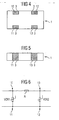
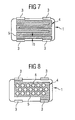
- Figures 7 and 8 show further embodiments of a resistor 4, as it could be used in place of the resistor 41 shown in Figure 1. Accordingly, Figure 7 shows a further meandering structure for the resistor 4.
- the layer 4 forming the resistor 4 is structured in the form of a meander.
- the meander is formed by a web with the width b, which may correspond to the width b of FIG.
- the meander in FIG. 7 does not run in the longitudinal direction of the main body 1, but in the transverse direction.
- a resistor 4 is shown, which is formed of a rectangular closed layer 5 by arranging recesses 6 in the layer 5. These recesses 6 may be circular, but they may also have other shapes, such as rectangles. By a uniform distribution of a plurality of recesses 6, the resistance of the originally rectangular layer 5 can be significantly increased. As an effect of the recesses 6 results in a plurality of multiply curved current paths between the external contacts 3, which have a high resistance.
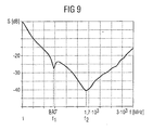
- FIG. 9 shows the insertion loss of the component shown in FIG. 2 or in FIG. 6.
- the insertion loss S is plotted in the unit dB over the frequency f [MHz].
- Resonance frequencies f 1 , f 2 are formed by the two capacitors C1, C2 contained in the varistors VDR1, VDR2. At the locations of the resonant frequencies f 1, f 2 the device exhibits an increased attenuation. Also between the resonant frequencies f 1 , f 2 , the device due to the ⁇ circuit realizing resistor R a very good attenuation, which is better than -20 dB in the frequency interval between 740 MHz and 2.7 GHz.
- the component is suitable for suppressing a frequency band which lies between the resonance frequencies f 1 (part of C1) and the resonance frequency f 2 (part of C2).
- the resistance R is 1.8 ⁇ in the embodiment shown in the figures.
Landscapes
- Engineering & Computer Science (AREA)
- Microelectronics & Electronic Packaging (AREA)
- Physics & Mathematics (AREA)
- Electromagnetism (AREA)
- Thermistors And Varistors (AREA)
- Fixed Capacitors And Capacitor Manufacturing Machines (AREA)
- Details Of Resistors (AREA)
- Coils Or Transformers For Communication (AREA)
- Control Of Motors That Do Not Use Commutators (AREA)
Applications Claiming Priority (3)
| Application Number | Priority Date | Filing Date | Title |
|---|---|---|---|
| DE10144364A DE10144364A1 (de) | 2001-09-10 | 2001-09-10 | Elektrisches Vielschichtbauelement |
| DE10144364 | 2001-09-10 | ||
| PCT/DE2002/002952 WO2003028045A2 (de) | 2001-09-10 | 2002-08-12 | Elektrisches vielschichtbauelement |
Publications (2)
| Publication Number | Publication Date |
|---|---|
| EP1425762A2 EP1425762A2 (de) | 2004-06-09 |
| EP1425762B1 true EP1425762B1 (de) | 2007-01-24 |
Family
ID=7698380
Family Applications (1)
| Application Number | Title | Priority Date | Filing Date |
|---|---|---|---|
| EP02754524A Expired - Lifetime EP1425762B1 (de) | 2001-09-10 | 2002-08-12 | Elektrisches vielschichtbauelement |
Country Status (8)
| Country | Link |
|---|---|
| US (1) | US7012501B2 (zh) |
| EP (1) | EP1425762B1 (zh) |
| JP (1) | JP4095961B2 (zh) |
| CN (1) | CN100490025C (zh) |
| AT (1) | ATE352847T1 (zh) |
| DE (2) | DE10144364A1 (zh) |
| TW (1) | TW569247B (zh) |
| WO (1) | WO2003028045A2 (zh) |
Families Citing this family (15)
| Publication number | Priority date | Publication date | Assignee | Title |
|---|---|---|---|---|
| DE10356498A1 (de) | 2003-12-03 | 2005-07-07 | Epcos Ag | Elektrisches Bauelement und Schaltungsanordnung |
| DE102004010001A1 (de) * | 2004-03-01 | 2005-09-22 | Epcos Ag | Elektrisches Bauelement und schaltungsanordnung mit dem Bauelement |
| US7763833B2 (en) * | 2004-03-12 | 2010-07-27 | Goodrich Corp. | Foil heating element for an electrothermal deicer |
| DE102004037588A1 (de) * | 2004-08-03 | 2006-02-23 | Epcos Ag | Elektrisches Bauelement und Verfahren zur Herstellung eines elektrischen Bauelements |
| JP4715248B2 (ja) * | 2005-03-11 | 2011-07-06 | パナソニック株式会社 | 積層セラミック電子部品 |
| US7923668B2 (en) * | 2006-02-24 | 2011-04-12 | Rohr, Inc. | Acoustic nacelle inlet lip having composite construction and an integral electric ice protection heater disposed therein |
| DE102006060634A1 (de) | 2006-12-21 | 2008-06-26 | Robert Bosch Gmbh | Verfahren zur Herstellung eines elektrischen Widerstands auf einem Substrat |
| DE102007046607A1 (de) * | 2007-09-28 | 2009-04-02 | Epcos Ag | Elektrisches Vielschichtbauelement sowie Verfahren zur Herstellung eines elektrischen Vielschichtbauelements |
| US8264816B2 (en) * | 2009-08-24 | 2012-09-11 | Kemet Electronics Corporation | Externally fused and resistively loaded safety capacitor |
| US20130058004A1 (en) * | 2011-09-01 | 2013-03-07 | Medtronic, Inc. | Feedthrough assembly including underfill access channel and electrically insulating material |
| EP2793539A4 (en) * | 2011-12-16 | 2016-03-23 | Epcos Ag | MULTI-LAYERED VITROCERAMIC SUBSTRATE HAVING INCORPORATED RESISTANCE |
| KR20150069901A (ko) * | 2013-12-16 | 2015-06-24 | 삼성전기주식회사 | 칩 저항기 |
| MA47214A (fr) * | 2017-01-06 | 2019-11-13 | Hyperwave Tech Llc | Élément chauffant pour un appareil de cuisson |
| CN107393784A (zh) * | 2017-09-07 | 2017-11-24 | 上海长园维安电子线路保护有限公司 | 一种可以耐受高压的自控制型保护器及其制备方法 |
| JP7027176B2 (ja) * | 2018-01-22 | 2022-03-01 | ラピスセミコンダクタ株式会社 | 半導体装置 |
Family Cites Families (28)
| Publication number | Priority date | Publication date | Assignee | Title |
|---|---|---|---|---|
| GB570026A (en) | 1943-12-14 | 1945-06-19 | Johnson Matthey Co Ltd | Improvements in or relating to the manufacture and production of electrical resistors with a low inductance |
| US3266005A (en) * | 1964-04-15 | 1966-08-09 | Western Electric Co | Apertured thin-film circuit components |
| US3846345A (en) * | 1969-10-06 | 1974-11-05 | Owens Illinois Inc | Electroconductive paste composition and structures formed therefrom |
| DE3125281A1 (de) | 1981-06-26 | 1983-01-13 | Siemens AG, 1000 Berlin und 8000 München | Elektrische bauelementekombination, insbesondere r-c-kombination |
| DE3336229A1 (de) | 1983-10-05 | 1985-04-25 | Resista Fabrik elektrischer Widerstände GmbH, 8300 Landshut | Verfahren zur wertjustierung von widerstaenden |
| US4568908A (en) * | 1984-12-24 | 1986-02-04 | General Electric Company | Compact resistor assembly |
| EP0211331A3 (en) * | 1985-08-02 | 1989-10-25 | Hitachi, Ltd. | Heat-sensitive recording head and method of manufacturing same |
| US4811164A (en) * | 1988-03-28 | 1989-03-07 | American Telephone And Telegraph Company, At&T Bell Laboratories | Monolithic capacitor-varistor |
| US4870746A (en) * | 1988-11-07 | 1989-10-03 | Litton Systems, Inc. | Method of making a multilayer printed circuit board having screened-on resistors |
| JPH02312203A (ja) * | 1989-05-26 | 1990-12-27 | Matsushita Electric Ind Co Ltd | 厚膜抵抗体のトリミング方法 |
| ES2079415T3 (es) * | 1989-10-26 | 1996-01-16 | Takeshi Ikeda | Filtro de ruidos lc. |
| JPH0833327B2 (ja) * | 1990-06-11 | 1996-03-29 | 株式会社村田製作所 | 温度センサ |
| JPH05275958A (ja) * | 1992-03-25 | 1993-10-22 | Murata Mfg Co Ltd | ノイズフィルタ |
| JP3097332B2 (ja) * | 1992-07-21 | 2000-10-10 | 株式会社村田製作所 | 積層型チップバリスタ |
| US5430429A (en) * | 1992-09-29 | 1995-07-04 | Murata Manufacturing Co., Ltd. | Ceramic resistor wherein a resistance film is embedded |
| US5379016A (en) * | 1993-06-03 | 1995-01-03 | E. I. Du Pont De Nemours And Company | Chip resistor |
| US5521576A (en) * | 1993-10-06 | 1996-05-28 | Collins; Franklyn M. | Fine-line thick film resistors and resistor networks and method of making same |
| JP3138631B2 (ja) * | 1996-01-26 | 2001-02-26 | 太陽社電気株式会社 | チップ抵抗器及びその製造方法 |
| US5815367A (en) * | 1996-03-11 | 1998-09-29 | Murata Manufacturing Co., Ltd. | Layered capacitors having an internal inductor element |
| DE19612841A1 (de) * | 1996-03-30 | 1997-10-02 | Abb Research Ltd | Strombegrenzender Widerstand mit PTC-Verhalten |
| JP3631341B2 (ja) * | 1996-10-18 | 2005-03-23 | Tdk株式会社 | 積層型複合機能素子およびその製造方法 |
| GB9623460D0 (en) * | 1996-11-09 | 1997-01-08 | Oxley Dev Co Ltd | Electronic components incorporating capacitors |
| JPH1116703A (ja) * | 1997-06-20 | 1999-01-22 | Shoei Chem Ind Co | 超低抵抗抵抗器 |
| US5889445A (en) * | 1997-07-22 | 1999-03-30 | Avx Corporation | Multilayer ceramic RC device |
| US6362723B1 (en) * | 1999-11-18 | 2002-03-26 | Murata Manufacturing Co., Ltd. | Chip thermistors |
| DE10108662A1 (de) * | 2000-02-23 | 2001-08-30 | Tyco Electronics Amp Gmbh | Leiterbahn auf einem Substrat |
| DE10064447C2 (de) | 2000-12-22 | 2003-01-02 | Epcos Ag | Elektrisches Vielschichtbauelement und Entstörschaltung mit dem Bauelement |
| EP1223591A3 (en) | 2001-01-11 | 2007-06-06 | Matsushita Electric Industrial Co., Ltd. | Multilayer electronic component and communication apparatus |
-
2001
- 2001-09-10 DE DE10144364A patent/DE10144364A1/de not_active Ceased
-
2002
- 2002-08-12 DE DE50209370T patent/DE50209370D1/de not_active Expired - Lifetime
- 2002-08-12 CN CNB028176863A patent/CN100490025C/zh not_active Expired - Fee Related
- 2002-08-12 JP JP2003531482A patent/JP4095961B2/ja not_active Expired - Fee Related
- 2002-08-12 WO PCT/DE2002/002952 patent/WO2003028045A2/de active IP Right Grant
- 2002-08-12 EP EP02754524A patent/EP1425762B1/de not_active Expired - Lifetime
- 2002-08-12 AT AT02754524T patent/ATE352847T1/de not_active IP Right Cessation
- 2002-08-12 US US10/488,518 patent/US7012501B2/en not_active Expired - Lifetime
- 2002-09-09 TW TW091120464A patent/TW569247B/zh active
Also Published As
| Publication number | Publication date |
|---|---|
| WO2003028045A3 (de) | 2003-12-04 |
| US7012501B2 (en) | 2006-03-14 |
| JP2005504438A (ja) | 2005-02-10 |
| CN1554101A (zh) | 2004-12-08 |
| US20040239476A1 (en) | 2004-12-02 |
| DE10144364A1 (de) | 2003-04-03 |
| EP1425762A2 (de) | 2004-06-09 |
| DE50209370D1 (de) | 2007-03-15 |
| WO2003028045A2 (de) | 2003-04-03 |
| TW569247B (en) | 2004-01-01 |
| ATE352847T1 (de) | 2007-02-15 |
| JP4095961B2 (ja) | 2008-06-04 |
| CN100490025C (zh) | 2009-05-20 |
Similar Documents
| Publication | Publication Date | Title |
|---|---|---|
| DE4008507C2 (de) | Laminiertes LC-Filter | |
| DE102009028629B4 (de) | Ultra-Breitband-Kondensator | |
| DE69627785T2 (de) | Laminierter Resonator und laminiertes Bandpassfilter damit | |
| DE102006000935B4 (de) | Monolithisches keramisches Bauelement und Verfahren zur Herstellung | |
| EP1425762B1 (de) | Elektrisches vielschichtbauelement | |
| EP1350257B1 (de) | Elektrisches vielschichtbauelement und entstörschaltung mit dem bauelement | |
| EP1606831B1 (de) | Elektrisches vielschichtbauelement | |
| DE2952441A1 (de) | Laminiertes elektronisches bauteil und verfahren zur herstellung solcher bauteile | |
| DE19628890A1 (de) | Elektronikteile mit eingebauten Induktoren | |
| EP1369880B1 (de) | Elektrisches Vielschichtbauelement und Schaltungsanordnung | |
| WO2006119753A2 (de) | Elektrisches durchführungsbauelement mit vielschichtstruktur und verfahren zu dessen herstellung | |
| DE2752333A1 (de) | Streifenleitungs-kondensator | |
| DE4420060C2 (de) | Streifenleitungsfilter | |
| EP1369881B1 (de) | Elektrisches Vielschichtbauelement | |
| DE102004010001A1 (de) | Elektrisches Bauelement und schaltungsanordnung mit dem Bauelement | |
| DE10064445A1 (de) | Elektrisches Vielschichtbauelement und Anordnung mit dem Bauelement | |
| EP1391898B1 (de) | Elektrisches Vielschichtbauelement | |
| EP2530690B1 (de) | Elektrisches Vielschichtbauelement sowie Verfahren zur Herstellung eines elektrischen Vielschichtbauelements | |
| EP1537655B1 (de) | Mehrfachresonanzfilter | |
| EP1560235B1 (de) | Elektrisches Vielschichtbauelement | |
| DE10136545B4 (de) | Elektrokeramisches Bauelement, Vielschichtkondensator und Verfahren zur Herstellung des Vielschichtkondensators | |
| DE102004029411B4 (de) | Keramischer Mehrschichtkondensator | |
| DE10057084B4 (de) | Chip-Thermistoren und Verfahren zum Herstellen derselben | |
| DE4410753C2 (de) | Kondensator-Array | |
| WO2003009311A1 (de) | Elektrokeramisches bauelement |
Legal Events
| Date | Code | Title | Description |
|---|---|---|---|
| PUAI | Public reference made under article 153(3) epc to a published international application that has entered the european phase |
Free format text: ORIGINAL CODE: 0009012 |
|
| 17P | Request for examination filed |
Effective date: 20040123 |
|
| AK | Designated contracting states |
Kind code of ref document: A2 Designated state(s): AT BE BG CH CY CZ DE DK EE ES FI FR GB GR IE IT LI LU MC NL PT SE SK TR |
|
| 17Q | First examination report despatched |
Effective date: 20050502 |
|
| GRAP | Despatch of communication of intention to grant a patent |
Free format text: ORIGINAL CODE: EPIDOSNIGR1 |
|
| GRAS | Grant fee paid |
Free format text: ORIGINAL CODE: EPIDOSNIGR3 |
|
| GRAA | (expected) grant |
Free format text: ORIGINAL CODE: 0009210 |
|
| AK | Designated contracting states |
Kind code of ref document: B1 Designated state(s): AT BE BG CH CY CZ DE DK EE ES FI FR GB GR IE IT LI LU MC NL PT SE SK TR |
|
| PG25 | Lapsed in a contracting state [announced via postgrant information from national office to epo] |
Ref country code: FI Free format text: LAPSE BECAUSE OF FAILURE TO SUBMIT A TRANSLATION OF THE DESCRIPTION OR TO PAY THE FEE WITHIN THE PRESCRIBED TIME-LIMIT Effective date: 20070124 Ref country code: DK Free format text: LAPSE BECAUSE OF FAILURE TO SUBMIT A TRANSLATION OF THE DESCRIPTION OR TO PAY THE FEE WITHIN THE PRESCRIBED TIME-LIMIT Effective date: 20070124 Ref country code: IE Free format text: LAPSE BECAUSE OF FAILURE TO SUBMIT A TRANSLATION OF THE DESCRIPTION OR TO PAY THE FEE WITHIN THE PRESCRIBED TIME-LIMIT Effective date: 20070124 Ref country code: NL Free format text: LAPSE BECAUSE OF FAILURE TO SUBMIT A TRANSLATION OF THE DESCRIPTION OR TO PAY THE FEE WITHIN THE PRESCRIBED TIME-LIMIT Effective date: 20070124 |
|
| REG | Reference to a national code |
Ref country code: GB Ref legal event code: FG4D Free format text: NOT ENGLISH |
|
| REG | Reference to a national code |
Ref country code: CH Ref legal event code: EP |
|
| REG | Reference to a national code |
Ref country code: IE Ref legal event code: FG4D Free format text: LANGUAGE OF EP DOCUMENT: GERMAN |
|
| REF | Corresponds to: |
Ref document number: 50209370 Country of ref document: DE Date of ref document: 20070315 Kind code of ref document: P |
|
| PG25 | Lapsed in a contracting state [announced via postgrant information from national office to epo] |
Ref country code: SE Free format text: LAPSE BECAUSE OF FAILURE TO SUBMIT A TRANSLATION OF THE DESCRIPTION OR TO PAY THE FEE WITHIN THE PRESCRIBED TIME-LIMIT Effective date: 20070424 |
|
| PG25 | Lapsed in a contracting state [announced via postgrant information from national office to epo] |
Ref country code: BG Free format text: LAPSE BECAUSE OF THE APPLICANT RENOUNCES Effective date: 20070425 |
|
| PG25 | Lapsed in a contracting state [announced via postgrant information from national office to epo] |
Ref country code: ES Free format text: LAPSE BECAUSE OF FAILURE TO SUBMIT A TRANSLATION OF THE DESCRIPTION OR TO PAY THE FEE WITHIN THE PRESCRIBED TIME-LIMIT Effective date: 20070505 |
|
| PG25 | Lapsed in a contracting state [announced via postgrant information from national office to epo] |
Ref country code: PT Free format text: LAPSE BECAUSE OF FAILURE TO SUBMIT A TRANSLATION OF THE DESCRIPTION OR TO PAY THE FEE WITHIN THE PRESCRIBED TIME-LIMIT Effective date: 20070625 |
|
| NLV1 | Nl: lapsed or annulled due to failure to fulfill the requirements of art. 29p and 29m of the patents act | ||
| GBV | Gb: ep patent (uk) treated as always having been void in accordance with gb section 77(7)/1977 [no translation filed] |
Effective date: 20070124 |
|
| REG | Reference to a national code |
Ref country code: IE Ref legal event code: FD4D |
|
| EN | Fr: translation not filed | ||
| PG25 | Lapsed in a contracting state [announced via postgrant information from national office to epo] |
Ref country code: SK Free format text: LAPSE BECAUSE OF FAILURE TO SUBMIT A TRANSLATION OF THE DESCRIPTION OR TO PAY THE FEE WITHIN THE PRESCRIBED TIME-LIMIT Effective date: 20070124 Ref country code: GB Free format text: LAPSE BECAUSE OF FAILURE TO SUBMIT A TRANSLATION OF THE DESCRIPTION OR TO PAY THE FEE WITHIN THE PRESCRIBED TIME-LIMIT Effective date: 20070124 |
|
| PLBE | No opposition filed within time limit |
Free format text: ORIGINAL CODE: 0009261 |
|
| STAA | Information on the status of an ep patent application or granted ep patent |
Free format text: STATUS: NO OPPOSITION FILED WITHIN TIME LIMIT |
|
| 26N | No opposition filed |
Effective date: 20071025 |
|
| PG25 | Lapsed in a contracting state [announced via postgrant information from national office to epo] |
Ref country code: CZ Free format text: LAPSE BECAUSE OF FAILURE TO SUBMIT A TRANSLATION OF THE DESCRIPTION OR TO PAY THE FEE WITHIN THE PRESCRIBED TIME-LIMIT Effective date: 20070124 |
|
| BERE | Be: lapsed |
Owner name: EPCOS A.G. Effective date: 20070831 |
|
| REG | Reference to a national code |
Ref country code: CH Ref legal event code: PL |
|
| PG25 | Lapsed in a contracting state [announced via postgrant information from national office to epo] |
Ref country code: LI Free format text: LAPSE BECAUSE OF NON-PAYMENT OF DUE FEES Effective date: 20070831 Ref country code: GR Free format text: LAPSE BECAUSE OF FAILURE TO SUBMIT A TRANSLATION OF THE DESCRIPTION OR TO PAY THE FEE WITHIN THE PRESCRIBED TIME-LIMIT Effective date: 20070425 Ref country code: FR Free format text: LAPSE BECAUSE OF FAILURE TO SUBMIT A TRANSLATION OF THE DESCRIPTION OR TO PAY THE FEE WITHIN THE PRESCRIBED TIME-LIMIT Effective date: 20070914 Ref country code: MC Free format text: LAPSE BECAUSE OF NON-PAYMENT OF DUE FEES Effective date: 20070831 Ref country code: IT Free format text: LAPSE BECAUSE OF FAILURE TO SUBMIT A TRANSLATION OF THE DESCRIPTION OR TO PAY THE FEE WITHIN THE PRESCRIBED TIME-LIMIT Effective date: 20070124 Ref country code: CH Free format text: LAPSE BECAUSE OF NON-PAYMENT OF DUE FEES Effective date: 20070831 |
|
| PG25 | Lapsed in a contracting state [announced via postgrant information from national office to epo] |
Ref country code: BE Free format text: LAPSE BECAUSE OF NON-PAYMENT OF DUE FEES Effective date: 20070831 |
|
| PG25 | Lapsed in a contracting state [announced via postgrant information from national office to epo] |
Ref country code: AT Free format text: LAPSE BECAUSE OF NON-PAYMENT OF DUE FEES Effective date: 20070812 Ref country code: FR Free format text: LAPSE BECAUSE OF FAILURE TO SUBMIT A TRANSLATION OF THE DESCRIPTION OR TO PAY THE FEE WITHIN THE PRESCRIBED TIME-LIMIT Effective date: 20070124 |
|
| PG25 | Lapsed in a contracting state [announced via postgrant information from national office to epo] |
Ref country code: EE Free format text: LAPSE BECAUSE OF FAILURE TO SUBMIT A TRANSLATION OF THE DESCRIPTION OR TO PAY THE FEE WITHIN THE PRESCRIBED TIME-LIMIT Effective date: 20070124 |
|
| PG25 | Lapsed in a contracting state [announced via postgrant information from national office to epo] |
Ref country code: CY Free format text: LAPSE BECAUSE OF FAILURE TO SUBMIT A TRANSLATION OF THE DESCRIPTION OR TO PAY THE FEE WITHIN THE PRESCRIBED TIME-LIMIT Effective date: 20070124 |
|
| PG25 | Lapsed in a contracting state [announced via postgrant information from national office to epo] |
Ref country code: LU Free format text: LAPSE BECAUSE OF NON-PAYMENT OF DUE FEES Effective date: 20070812 |
|
| PG25 | Lapsed in a contracting state [announced via postgrant information from national office to epo] |
Ref country code: TR Free format text: LAPSE BECAUSE OF FAILURE TO SUBMIT A TRANSLATION OF THE DESCRIPTION OR TO PAY THE FEE WITHIN THE PRESCRIBED TIME-LIMIT Effective date: 20070124 |
|
| REG | Reference to a national code |
Ref country code: DE Ref legal event code: R082 Ref document number: 50209370 Country of ref document: DE Representative=s name: EPPING HERMANN FISCHER PATENTANWALTSGESELLSCHA, DE Ref country code: DE Ref legal event code: R081 Ref document number: 50209370 Country of ref document: DE Owner name: TDK ELECTRONICS AG, DE Free format text: FORMER OWNER: EPCOS AG, 81669 MUENCHEN, DE |
|
| PGFP | Annual fee paid to national office [announced via postgrant information from national office to epo] |
Ref country code: DE Payment date: 20210825 Year of fee payment: 20 |
|
| REG | Reference to a national code |
Ref country code: DE Ref legal event code: R071 Ref document number: 50209370 Country of ref document: DE |