EP1420357A1 - Procédé pour adapter la caractéristique de couplage electromagnétique dans un système d'alimentation électrique sans contact et système d'alimentation électrique sans contact - Google Patents
Procédé pour adapter la caractéristique de couplage electromagnétique dans un système d'alimentation électrique sans contact et système d'alimentation électrique sans contact Download PDFInfo
- Publication number
- EP1420357A1 EP1420357A1 EP03257108A EP03257108A EP1420357A1 EP 1420357 A1 EP1420357 A1 EP 1420357A1 EP 03257108 A EP03257108 A EP 03257108A EP 03257108 A EP03257108 A EP 03257108A EP 1420357 A1 EP1420357 A1 EP 1420357A1
- Authority
- EP
- European Patent Office
- Prior art keywords
- power supply
- power
- antenna coil
- semiconductor device
- electromagnetic coupling
- Prior art date
- Legal status (The legal status is an assumption and is not a legal conclusion. Google has not performed a legal analysis and makes no representation as to the accuracy of the status listed.)
- Granted
Links
Images


Classifications
-
- G—PHYSICS
- G06—COMPUTING; CALCULATING OR COUNTING
- G06K—GRAPHICAL DATA READING; PRESENTATION OF DATA; RECORD CARRIERS; HANDLING RECORD CARRIERS
- G06K17/00—Methods or arrangements for effecting co-operative working between equipments covered by two or more of main groups G06K1/00 - G06K15/00, e.g. automatic card files incorporating conveying and reading operations
-
- G—PHYSICS
- G06—COMPUTING; CALCULATING OR COUNTING
- G06K—GRAPHICAL DATA READING; PRESENTATION OF DATA; RECORD CARRIERS; HANDLING RECORD CARRIERS
- G06K19/00—Record carriers for use with machines and with at least a part designed to carry digital markings
- G06K19/06—Record carriers for use with machines and with at least a part designed to carry digital markings characterised by the kind of the digital marking, e.g. shape, nature, code
- G06K19/067—Record carriers with conductive marks, printed circuits or semiconductor circuit elements, e.g. credit or identity cards also with resonating or responding marks without active components
- G06K19/07—Record carriers with conductive marks, printed circuits or semiconductor circuit elements, e.g. credit or identity cards also with resonating or responding marks without active components with integrated circuit chips
- G06K19/0701—Record carriers with conductive marks, printed circuits or semiconductor circuit elements, e.g. credit or identity cards also with resonating or responding marks without active components with integrated circuit chips at least one of the integrated circuit chips comprising an arrangement for power management
- G06K19/0715—Record carriers with conductive marks, printed circuits or semiconductor circuit elements, e.g. credit or identity cards also with resonating or responding marks without active components with integrated circuit chips at least one of the integrated circuit chips comprising an arrangement for power management the arrangement including means to regulate power transfer to the integrated circuit
-
- H—ELECTRICITY
- H02—GENERATION; CONVERSION OR DISTRIBUTION OF ELECTRIC POWER
- H02J—CIRCUIT ARRANGEMENTS OR SYSTEMS FOR SUPPLYING OR DISTRIBUTING ELECTRIC POWER; SYSTEMS FOR STORING ELECTRIC ENERGY
- H02J50/00—Circuit arrangements or systems for wireless supply or distribution of electric power
- H02J50/10—Circuit arrangements or systems for wireless supply or distribution of electric power using inductive coupling
- H02J50/12—Circuit arrangements or systems for wireless supply or distribution of electric power using inductive coupling of the resonant type
Definitions
- the present invention relates to a non-contact power supply system, which includes a semiconductor device such as an IC card and a power supply device for supplying power to the semiconductor device through electromagnetic coupling without contact with the semiconductor, and the power supply system used in the system, and further relates to an electromagnetic coupling characteristic adjustment method for the non-contact power supply system.
- an IC card has come into wide use, which is made of a plastic card containing such as an IC chip of a non-volatile memory, a CPU (Central Processing Unit) etc.
- the IC card is more advantageous in terms of handling of large amount of data, security, etc. than a magnetic card, which has been commonly used. With such advantages, much attention is now focused on an IC card as a new type card for the next generation.
- the reason for rapid widespread of an IC card is compatibility with various applications.
- the IC card can carry out not only applications currently enforced by a magnetic card, but also applications which cannot be enforced by a magnetic card due to technical limit. Also, there has been expectation for a multi-purpose IC card capable of having plural applications in a single card.
- the IC card uses a reader/writer device for power supply and writing of information.
- the IC card and the reader/writer device fall into contact-type and non-contact-type depending on their interfaces.
- each of the IC card and the reader-writer device includes a metal connection terminal, and data exchange is performed by bringing the connection terminal of the IC card into contact with the connection terminal of the reader/writer device. Bringing the respective connection terminals into contact also enables power supply from the reader/writer device to the IC card.
- each of the IC card and the reader-writer device includes an antenna coil.
- the antenna coil of the reader-writer device generates a variable electric field
- the antenna coil of the IC card enters the generated variable electric field so as to allow the reader-writer device to supply power to the IC card by electromagnetic induction technology and also allow data transmission between the reader-writer device and the IC card.
- the non-contact-type IC card rectifies an induced voltage generated in the antenna coil at a diode bridge before supplying the voltage to respective function blocks. Note that, in this manner, propagation between the antenna coil of the non-contact reader/writer device and the antenna coil of the non-contact IC card is carried out with an electromagnetic wave having a carrier frequency of in a range from several MHz to several 10MHz, for example.
- the non-contact IC card does not include a connection terminal for an external device, and therefore no concern is necessary for breakage of connection portion or the like. Further, the non-contact IC card is capable of power supply and data exchange with respect to the non-contact reader-writer device by only coming closer to the non-contact reader-writer device. Accordingly, the non-contact IC card is advantageous in terms of reduction of maintenance cost, easy handling, high-speed processing etc.
- the non-contact reader/writer device falls roughly into two structures depending on whether or not the device has a function for fixing the non-contact IC card.
- the former is referred to as a close-type, while the latter is referred to as an open-type.
- the communication distance between the close-type reader/writer device and IC card is not more than 5mm, and is often 1mm.
- Such a short distance of the close-type reader/writer device and IC card appeals to financial fields in which security of information plays an important role. For this reason, a conventional market has a stronger demand for a close-type reader/writer device than an open-type device.
- the IC card is more often used in traffic fields and also as a system for supervising entry/leaving of a room, and therefore, demand for the open-type with superior convenience increased to be greater than that for the close-type.
- One example can be a train ticket or a bus ticket made of an IC card, which is used by being held up by the user toward a ticket gate having an open-type reader/writer device, so as to allow the device to carry out data processing with the IC card ("hold up" data processing). Otherwise, the IC card is instantaneously brought into contact with the ticket gate ("touch and go" data processing).
- Figure 8 shows a relation between the communication distance from an open-type reader/writer device to an IC card, and power received by the IC card, when the power supply of the open-type reader/writer device is fixed.
- the power received by the IC card becomes maximum when the communication distance is 0, and then gradually decreases as the communication distance increases.
- an IC card closer to the reader/writer device receives more power.
- the difference of received power is converted into heat, thus causing heat generation of the IC card when the card is placed close to the reader/writer device for a long time.
- the power from the reader/writer device has to be increased, since the multi-purpose card requires a larger minimum voltage for driving than that of a conventional card due to its non-volatile memory of not less than 1MB consuming great power.
- Figure 9 shows a relation between the communication distance and the received power by the IC card when more power is supplied from the open-type reader/writer device.
- the received power can be increased by supplying larger power if the communication distance between the IC card and the reader/writer device is fixed.
- FIG. 7 shows an arrangement example of the reader/writer device and the IC card disclosed in the foregoing publication.
- the left side of the broken line shows an arrangement example of a reader/writer device 100 and the right side shows an arrangement example of an IC card 101.
- the reader/writer device 100 includes an oscillator 110, a power control circuit 111, an amplifier 112, a matching circuit 113, a voltage detection circuit 114, a reader/writer IC 115, a tuning capacitor 116, and an antenna coil 117.
- the oscillator 110 outputs a high frequency wave, which is amplified through the amplifier 112, so as to be supplied to the antenna coil 117 via the matching circuit 113.
- the antenna coil 117 is directly connected to the tuning capacitor 116 so as to increase transmission efficiency. Note that, in the circuit diagram of Figure 7, the antenna coil 117 is made up of an inductance component L1 and a resistance component R1.
- the IC card 101 includes an antenna coil 120, a tuning capacitor 121, a rectification circuit section 122, and an IC card logic section 123.
- the tuning capacitor 121 is connected in parallel with the antenna coil 120 as with the tuning capacitor 116 connected to the reader writer device 100, so as to increase transmission efficiency sympathetically with a self-inductance L2 of the antenna coil 120.
- Electromagnetic coupling of the antenna coil 120 of the IC card 101 and the antenna coil 117 of the reader/writer device 100 generates an induced voltage, which is then rectified through the rectification circuit section 122 and adjusted to be a predetermined voltage before supplying to the IC card logic section 123.
- the reader/writer device 100 is characterized by including a power control circuit 111 for controlling power supply to the antenna coil 117, a voltage detection circuit 114 for detecting an input voltage of the antenna coil 117, and first and second tables stored in the reader/writer IC 115.
- the first table is to derive a coupling coefficient k from an output voltage Vs of the power control circuit 111 and an input voltage V to the antenna coil detected by the voltage detection circuit 114.
- the second table is to derive an optimal (a voltage not causing excess heat) voltage Vs for the coupling coefficient k from the coupling coefficient k and an optimal received power P.
- the voltage detection circuit 114 detects an output voltage V (input voltage to the antenna coil 117) of the amplifier 112 at a certain timing.
- the detected value of the output voltage V is sent to the reader/writer IC 115. Since the reader/writer IC 115 controls the output voltage Vs of the power control circuit 111, it has already obtained the value of the output voltage Vs at this stage.
- the reader/writer IC 115 obtains the coupling coefficient k with reference to the first table by using the output voltage V of the amplifier 112 and the output voltage Vs of the power control circuit 111. Then, the reader/writer IC 115 obtains an optimal (a voltage not causing excess heat) output voltage Vs of the power control circuit 111 for the coupling coefficient k with reference to the second table by using the coupling coefficient k which has been obtained and the optimal received power P for the IC card.
- the reader/writer IC 115 controls the power control circuit 111 so that the power control circuit 111 outputs the obtained output voltage Vs. Consequently, it is possible to cut the excess power supply and prevent heat generation due to the power difference.
- the foregoing IC card 101 and the reader/writer device 100 which can prevent heat generation due to the power difference of the received power however causes magnification of circuit scale and an increase of power consumption because of provision of the power control circuit 111 and the voltage detection circuit 114.
- the IC card 101 and the reader/writer device 100 still require an increase of power supply when extending the communication distance. Therefore, the problem of adverse effect to the other devices due to an increase of power supply still cannot be solved.
- the present invention is made in view of the foregoing conventional problems, and an object is to provide a non-contact power supply system having a simple structure and capable of reducing heat generation due to difference in received power. Further, another object of the present invention is to provide a non-contact power supply system capable of extending an allowable operation distance between a semiconductor device and a power supply device without increasing power supply from the power supply device.
- an electromagnetic coupling characteristic adjustment method of the present invention for adjusting an electromagnetic coupling characteristic between a power supply device and a semiconductor device which are used in a non-contact power supply system in which a power transmission antenna coil provided in the power supply device and a power receiving antenna coil provided in the semiconductor device are electromagnetically coupled so that the power supply device supplies power to the semiconductor device without contact with the semiconductor device
- the power supply device includes a first adjustment impedance element connected in series to the power transmission antenna coil and a second adjustment impedance element connected in parallel with the power transmission antenna coil.
- the electromagnetic coupling characteristic adjustment method comprising the step of: (a) determining impedances of the first and second adjustment impedance elements so that the semiconductor device receives greatest power when a power supply distance, which is a distance between the power transmission antenna coil and the power receiving antenna coil, has a predetermined value not less than 0.
- the predetermined value of the power supply distance is preferably in the vicinity of a likely power supply distance used for the system.
- a non-contact communication system where the semiconductor device is an IC card and the power supply device is a reader/writer device, falls into a close-type, an adjacent-type, a proximity-type, according to a communication distance between the IC card and the reader/writer device.
- These different types are in progress for standardization as ISO10536, ISO/IEC14443, and ISO/IEC15693, with likely communication distances of 1mm (millimeter), around 100mm, and around 700mm, respectively.
- the predetermined value of power supply distance is preferably around 1mm in a close-type, around 100mm in an adjacent-type, and around 700mm in a proximity type, in case of a non-contact communication system. Further, the predetermined value of communication distance is more preferably in the vicinity of 30mm, specifically in a range between 20mm to 40mm, which is most likely communication distance used for the adjacent-type IC card.
- the impedances of the first and second impedance adjustment elements in the power supply device are determined so that the semiconductor device receives greatest power at a predetermined value of communication distance.
- variation quantity of the dependent variable y is small in the vicinity of the local maximum and the local minimum.
- the dependent variable y includes the local maximum or the local minimum in its range, the dependent variable increases and also decreases, and the range becomes smaller. Namely, for a variable varies in a predetermined range, a variable including the local maximum or the local minimum generally has a smaller range of dependent variable than a variable monotonically increases or monotonically decreases.
- variation of the received power due to difference of power supply distance can be reduced, compared to a conventional method in which the received power becomes maximum when a power supply distance is 0, and then monotonically decreases as the power supply distance increases.
- heat generation due to the difference of received power can be reduced with a simple structure only provided with the first and second adjustment impedance elements.
- the foregoing structure allows such extension with a smaller difference between the extended power supply distance and a power supply distance where the received power becomes maximum, thus offering greater received power at the extended power supply distance than the conventional system. Consequently, it is possible to extend the power supply distance without increasing power supply.
- an electromagnetic coupling characteristic adjustment method of the present invention for adjusting an electromagnetic coupling characteristic between a power supply device and a semiconductor device which are used in a non-contact power supply system in which a power transmission antenna coil provided in the power supply device and a power receiving antenna coil provided in the semiconductor device are electromagnetically coupled so that the power supply device supplies power to the semiconductor device without contact with the semiconductor device, the power supply device includes a first adjustment impedance element connected in series to the power transmission antenna coil and a second adjustment impedance element connected in parallel with the power transmission antenna coil, the electromagnetic coupling characteristic adjustment method comprising the step of: (a) determining impedances of the first and second adjustment impedance elements so that the semiconductor device receives greater power than a minimum power for operation of the semiconductor device when a power supply distance, which is a distance between the power transmission antenna coil and the power receiving antenna coil, is within a predetermined range.
- the impedances of the first and second adjustment impedance elements are determined so that the semiconductor device receives greater power than a minimum power for operation of the semiconductor device when a power supply distance is within a predetermined range. Also, in this case, the difference of received power due to variation of power supply distance can be reduced compared to the conventional method, thus reducing heat generation due to the difference of received power with a simple structure only provided with the first and second adjustment impedance elements.
- a power supply device of the present invention including a power transmission antenna coil which is electromagnetically coupled with a power receiving antenna coil provided in a semiconductor device so as to supply power to the semiconductor device without contact with the semiconductor device, includes: a first adjustment impedance element connected in series to the power transmission antenna coil; and a second adjustment impedance element connected in parallel with the power transmission antenna coil, impedances of the first and second adjustment impedance elements being determined so that the semiconductor device receives greatest power when a power supply distance, which is a distance between the power transmission antenna coil and the power receiving antenna coil, is within a predetermined range whose lower limit is greater than 0.
- the first and second adjustment impedance elements are determined so that the semiconductor device receives greatest power at a power supply distance of greater than 0.
- the difference of received power due to variation of power supply distance can be reduced compared to the conventional method, thus reducing heat generation due to the difference of received power with a simple structure only provided with the first and second adjustment impedance elements.
- the foregoing structure allows such extension with a smaller difference between the extended power supply distance and a power supply distance where the received power becomes maximum, thus offering greater received power at the extended power supply distance than the conventional system. Consequently, it is possible to extend the power supply distance without increasing power supply.
- a non-contact power supply system includes a power supply device having the foregoing structure and a semiconductor device having a power receiving antenna coil which is electromagnetically coupled with a power transmission antenna coil of the power supply device.
- Figure 3 shows an arrangement example of a circuit for a non-contact IC card system used in the present embodiment.
- the left side of the broken line shows an arrangement example of a reader/writer device (power supply device) 1 and the right side shows an arrangement example of an IC card (semiconductor device) 2.
- the reader/writer device 1 includes an oscillator (power supplying section) 10, an amplifier (power supplying section) 11, adjustment capacitors 12 and 13, and an antenna coil 14.
- the oscillator 10 outputs a high frequency wave, which is then amplified through the amplifier 11 so as to be supplied to the antenna coil 14.
- the antenna coil 14 is connected in series to the adjustment capacitor (first adjustment impedance element) 12, and also connected in parallel with the adjustment capacitor (second adjustment impedance element) 13.
- the IC card 2 includes an antenna coil 20, a tuning capacitor 21, a rectification circuit section 22, and an IC card logic section 23.
- the tuning capacitor 21 is connected in parallel with the antenna coil 20 so as to increase transmission efficiency sympathetically with a self-inductance L2 of the antenna coil 20. Electromagnetic coupling of the antenna coil 20 of the IC card 2 and the antenna coil 14 of the reader/writer device 1 generates an induced voltage, which is then rectified through the rectification circuit section 22 and adjusted to be a predetermined voltage before supplying to the IC card logic section 23.
- the non-contact IC card system of the present embodiment is an adjacent-type with a communication distance of from 0mm to 50mm.
- the following will explain a calculation method of an electromagnetic coupling characteristic between the antenna coil 14 of the reader/writer device 1 and the antenna coil 20 of the IC card 2. Note that, since the electromagnetic coupling characteristic changes depending on the shapes of the antenna coils 14 and 20, it is assumed in the following explanation that the shapes of those are fixed.
- the present embodiment uses the following procedures so as to increase the communication distance from 0mm to 50mm.
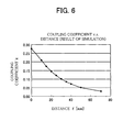
- the coupling coefficient k changes depending on geometric arrangement of the antennal coil 14 with respect to the antenna coil 20, and therefore the coupling coefficient k can be found out by simulation or the like. Further, since the shapes of the antenna coils 14 and 20 are fixed, the coupling coefficient k depends on a communication distance l .
- Figure 6 shows a relation between the coupling coefficient k and the communication distance l .
- the coupling coefficient k is a function monotonically decreases with respect to the communication distance l , i.e., the coupling coefficient k is uniquely fixed with respect to the communication distance l . Accordingly, when the communication distance l is determined, the range of the coupling coefficient k is uniquely fixed.
- the coupling coefficient k is in a range from 0.05 to 0.27 when the communication distance l is in a range from 0mm to 50mm. Then, the capacitances CA and CB are determined so that the power receiving becomes maximum when the coupling coefficient k is within the foregoing range.
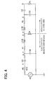
- This calculation uses an electromagnetic coupling equivalent circuit shown in Figure 4, which corresponds to the system arrangement of the present embodiment.
- FIGS 4 and 5 show an electromagnetic coupling equivalent circuit for the reader/writer device 1 and the IC card 2.
- a resistance RL is a maximum load resistance of a semiconductor device included in the IC card 2, and the resistance value thereof is found according to an operation current value of the semiconductor device used for the IC card 2.
- the resistance RL is supplied with a voltage VB in its both ends.
- the voltage VB is generated by power received in the IC card 2 upon electromagnetic coupling of the reader/writer device 1 and the IC card 2.
- a capacitor C2 is provided as a capacitance of the tuning capacitor 21 connected in parallel with the antenna coil 20, and a capacitor C3 is an internal capacitance of the chip in this example, which is however not necessarily provided inside the chip. In the present embodiment, it is not necessary to change the coil constant of the antenna coil 20 of the IC card 2, and therefore, the value of the capacitor C2 is appropriately determined according to the coil constant mounted in the IC card 2.
- the resistance R2 is a loss resistance of the antenna coil 20, and an inductance L2 is a self inductance of the antenna coil 20.
- the resistance R2 and the inductance L2-M are determined as specific values according to the coil constant, for the same reason above.
- the inductance L1 is a self inductance of the antenna coil 14 of the reader/writer device 1, and the resistance R1 is a loss resistance of the antenna coil 14.
- the resistance R1 and the inductance L1-M are determined as specific values according to the coil constant, for the same reason above.
- the capacitances CA and CB of the adjustment capacitors 12 and 13, and the coupling coefficient k operate as variation parameters for the received power PB supplied to the resistance RL, i.e., the received power of the IC card 2.
- the output resistance R0 of the amplifier 11 of the reader/writer device 1 is determined as 50 ⁇ . It should be noted that the same calculation can be used when the output resistance R0 is an impedance with an imaginary component (R+jX).
- the schematic view of Figure 5 includes points A, G, E, C, and B, and respective impedance from those points toward the IC card side are described as ZA, ZG, ZE, ZC and ZB.
- the function fA can be found by setting substitute values for the coil constant (L1, L2, R1, R2, C2), the IC card-side constant RL, and C3.
- ZB and ZC are constants
- ZE is a function with k as a variable
- ZG is a function with CB and k as variables.
- VA V0 (ZA/(R0 + ZA))
- VG VA (ZG/((1/jwCA) + ZG)
- a voltage VE at the point E (point D) is found by dividing the voltage VG at the point G (point F) by R1, an impedance of (L1-M) and ZE, which is expressed as follows.
- VE VG (ZE/(R1 + jw (L1-M) + ZE)
- a voltage VC at the point C is found by dividing the voltage VE at the point E (point D) by R2, an impedance of (L2-M) and ZC, which is expressed as follows.
- VC VE (ZC/(R2 + jw (L2-M) + ZC)
- a voltage VB at the point B is found by dividing the voltage VC at the point C by an impedance (1/jwC3) of C3 and RL, which is expressed as follows.
- VB VC (RL/ (( 1/jwC3) + RL)
- PB VB 2 / RL
- the formula 6 can be expressed as the following function f2 with CA, CB and k as variables.
- PB f2 (CA, CB, k )
- Figure 1 shows a relation between communication distance and received power when the coil constants of the reader/writer side and the IC card side are determined by the foregoing adjustment.
- the vertical axis shows received power of the IC card 2
- the received power A1 shows power consumed by the semiconductor device for the IC card.
- the received power A1 shows the minimum power for driving a non-contact-type IC card. Accordingly, the IC card 2 does not start operation when the received power is less than A1.
- the horizontal axis shows a coupling coefficient k .
- the coupling coefficient k is a function which monotonically decreases with respect to the communication distance l , and therefore, the communication distance l decreases as the coupling coefficient k increases.
- the curved line a shows characteristic of received power in a conventional system.
- the received power decreases as the communication distance increases, and drops lower than the power consumption of the semiconductor device at the communication distance of 15mm. It reveals that the maximum communication distance is approximately 15mm.
- heat generation occurs by extra power (A2-A1), but the amount thereof is within a range for allowing the IC card 2 to operate without malfunction.
- the received power characteristic changes in the vertical direction when the output voltage V0 of the reader/writer device 1 is changed.
- the output voltage V0 of the reader/writer device 1 is adjusted so as to obtain the received power A1 at communication distances of 0mm and of 50mm.
- the power supply from the oscillator 10 and the amplifier 11 to the antenna coil 14 is adjusted so that the received power becomes higher than the minimum power for driving the IC card 2.
- the foregoing communication distance can be frequently used.
- the communication distance exceeds 50mm, the received power becomes lower than the minimum driving voltage. Accordingly, this distance is considered the maximum communication distance under the condition with the foregoing adjustment.
- impedance is adjusted to have the received power characteristic shown by a curved line c of Figure 1, so that an IC card specification can be made with a specific communication distance.
- the coupling coefficient k i.e., the communication distance l for the maximum received power changes depending on the capacitance CB.
- the IC card 2 receives maximum power near the reader/writer device 1, thus attaining a limited, though significant increase in the communication distance.
- the adjustment of the peak value of the received power characteristic may depend on the specification of power consumption of a semiconductor device used for the IC card 2, and the specification of communication distance of the non-contact IC card system.
- the example of Figure 2 adjusts impedance by fixing the capacitance CA of the adjustment capacitor 12 and changing the capacitance CB of the adjustment capacitor 13; however, the adjustment of impedance may also be performed by fixing the capacitance CB and changing the capacitance CA, or by changing both the capacitances CA and CB.
- the present embodiment describes a non-contact IC card system with the reader/writer device 1 including the adjustment capacitors 12 and 13
- the present invention may also be adopted for a non-contact IC card system using a reader/writer device 1 including other impedance element than the adjustment capacitors 12 and 13, for example, a coil or the like.
- the present invention may be adopted for the whole of RF communication by electromagnetic induction, such as a non-contact tag.
- the foregoing embodiment describes an example of performing data communication between the reader/writer device supplying power and the IC card receiving the power; however, the present invention may also be adopted for a power supply system from a power supply device to a semiconductor device without performing communication.
- an electromagnetic coupling characteristic adjustment method for adjusting an electromagnetic coupling characteristic between a power supply device and a semiconductor device which are used in a non-contact power supply system in which a power transmission antenna coil provided in the power supply device and a power receiving antenna coil provided in the semiconductor device are electromagnetically coupled so that the power supply device supplies power to the semiconductor device without contact with the semiconductor device, the power supply device includes a first adjustment impedance element connected in series to the power transmission antenna coil and a second adjustment impedance element connected in parallel with the power transmission antenna coil, the electromagnetic coupling characteristic adjustment method comprising the step of: (a) determining impedances of the first and second adjustment impedance elements so that the semiconductor device receives greatest power when a power supply distance, which is a distance between the power transmission antenna coil and the power receiving antenna coil, has a predetermined value not less than 0.
- the difference of received power due to variation of power supply distance can be reduced compared to the conventional method, thus reducing heat generation due to the difference of received power with a simple structure only provided with the first and second adjustment impedance elements.
- the power supply distance from the power supply device is extended while enabling operation of the semiconductor device, it is possible in this method to obtain greater received power in the extended distance than that of the conventional method, thus allowing extension of distance without increasing power supply.
- the electromagnetic coupling characteristic adjustment method of the present invention in a non-contact power supply system as set forth in claim 1 is arranged so that the step (a) includes the sub-steps of: determining a relation between (i) an electromagnetic coupling coefficient for the power transmission antenna coil and the power receiving antenna coil, and (ii) the power supply distance; and determining impedances of the first and second adjustment impedance elements so that the semiconductor device receives the greatest power when an electromagnetic coupling coefficient becomes a value corresponding to the predetermined value of the power supply distance.
- An electromagnetic coupling coefficient depends on geometric arrangement of the respective antenna coils. Therefore, the power supply distance may correspond to the electromagnetic coupling coefficient. Further, the relation between the electromagnetic coupling coefficient and the received power can be easily found by using an equivalent circuit diagram.
- impedance of the adjustment impedance element can be easily determined by finding the relation between the electromagnetic coupling coefficient and the power supply distance.
- the electromagnetic coupling characteristic adjustment method of the present invention in a non-contact power supply system further includes the step of: (b) determining power supplied from the power supply device so that the semiconductor device receives greater power than a minimum power for operation of the semiconductor device when the power supply distance is within a predetermined range.
- the predetermined range of power supply distance is preferably equal to a range of power supply distance likely used for the system.
- the preferable range is not more than 5mm for the close-type, not more than 100mm for the adjacent-type, and not more than 700mm for the proximity-type.
- the lower limit of power supply distance is fixed as 0, and therefore an increase of power supply only causes an increase of the upper limit of the range of power supply distance.
- an increase of power supply causes an increase of the upper limit of the range of power supply distance and also causes a decrease of the lower limit of the range. Therefore, the foregoing method allows a larger increase of the range of power supply distance than the conventional method with a small increase of power supply, thus easily finding a specific power supply value causing the semiconductor device to receive greater power than a minimum power for operation of the semiconductor device when the power supply distance is within a predetermined range.
- the power supply device includes a first adjustment impedance element connected in series to the power transmission antenna coil and a second adjustment impedance element connected in parallel with the power transmission antenna coil.
- the electromagnetic coupling characteristic adjustment method comprising the step of: (a) determining impedances of the first and second adjustment impedance elements so that the semiconductor device receives greater power than a minimum power for operation of the semiconductor device when a power supply distance, which is a distance between the power transmission antenna coil and the power receiving antenna coil, is within a predetermined range.
- the difference of received power due to variation of power supply distance can be reduced compared to the conventional method, thus reducing heat generation due to the difference of received power with a simple structure only provided with the first and second adjustment impedance elements.
- the electromagnetic coupling characteristic adjustment method of the present invention in a non-contact power supply system is arranged so that the step (a) includes the sub-steps of: determining a relation between (i) an electromagnetic coupling coefficient for the power transmission antenna coil and the power receiving antenna coil, and (ii) the power supply distance; and determining impedances of the first and second adjustment impedance elements so that the semiconductor device receives the greater power than a minimum power for operation of the semiconductor device when an electromagnetic coupling coefficient becomes a value corresponding to the predetermined range of the power supply distance.
- impedance of the adjustment impedance element can be easily determined by finding the relation between the electromagnetic coupling coefficient and the power supply distance.
- the first and second adjustment impedance elements are capacitors.
- the power supply device includes a first adjustment impedance element connected in series to the power transmission antenna coil and a second adjustment impedance element connected in parallel with the power transmission antenna coil.
- the impedances of the first and second adjustment impedance elements are determined so that the semiconductor device receives greatest power when the power supply distance is within a predetermined range whose lower limit is greater than 0.
- the difference of received power due to variation of power supply distance can be reduced compared to the conventional method, thus reducing heat generation due to the difference of received power with a simple structure only provided with the first and second adjustment impedance elements.
- the foregoing structure allows such extension with a smaller difference between the extended power supply distance and a power supply distance where the received power becomes maximum, thus offering greater received power at the extended power supply distance than the conventional system. Consequently, it is possible to extend the power supply distance without increasing power supply.
- the foregoing power supply device of the present invention is arranged so that power supplied to the power transmission antenna coil is determined so that the semiconductor device receives greater power than a minimum power for operation of the semiconductor device when the power supply distance is within the predetermined range.
- the foregoing method allows a larger increase of the range of power supply distance than the conventional method with a small increase of power supply, thus easily finding a specific power supply value causing the semiconductor device to receive greater power than a minimum power for operation of the semiconductor device when the power supply distance is within a predetermined range.
- the first and second adjustment impedance elements are capacitors.
- a non-contact power supply system includes a power supply device having the foregoing structure and a semiconductor device having a power receiving antenna coil which is electromagnetically coupled with a power transmission antenna coil of the power supply device.
Applications Claiming Priority (2)
| Application Number | Priority Date | Filing Date | Title |
|---|---|---|---|
| JP2002328836A JP2004166384A (ja) | 2002-11-12 | 2002-11-12 | 非接触型給電システムにおける電磁結合特性調整方法、給電装置、および非接触型給電システム |
| JP2002328836 | 2002-11-12 |
Publications (2)
| Publication Number | Publication Date |
|---|---|
| EP1420357A1 true EP1420357A1 (fr) | 2004-05-19 |
| EP1420357B1 EP1420357B1 (fr) | 2006-06-14 |
Family
ID=32171370
Family Applications (1)
| Application Number | Title | Priority Date | Filing Date |
|---|---|---|---|
| EP03257108A Expired - Fee Related EP1420357B1 (fr) | 2002-11-12 | 2003-11-11 | Procédé pour adapter la caractéristique de couplage electromagnétique dans un système d'alimentation électrique sans contact et système d'alimentation électrique sans contact |
Country Status (8)
| Country | Link |
|---|---|
| US (1) | US6889905B2 (fr) |
| EP (1) | EP1420357B1 (fr) |
| JP (1) | JP2004166384A (fr) |
| KR (1) | KR100642189B1 (fr) |
| CN (1) | CN1501566A (fr) |
| DE (1) | DE60306073T2 (fr) |
| SG (1) | SG111168A1 (fr) |
| TW (1) | TWI232410B (fr) |
Cited By (9)
| Publication number | Priority date | Publication date | Assignee | Title |
|---|---|---|---|---|
| WO2009144354A3 (fr) * | 2008-05-28 | 2010-02-18 | Fundación Circe- Centro De Investigación De Recursos Y Consumos Energéticos | Système de transfert de puissance à couplage inductif en haute fréquence et procédé associé |
| WO2011019088A3 (fr) * | 2009-08-13 | 2011-09-09 | Panasonic Corporation | Unité de transmission d'énergie sans fil, générateur d'énergie et système de production d'énergie muni de cette unité de transmission d'énergie sans fil |
| CN102647015A (zh) * | 2012-04-24 | 2012-08-22 | 深圳市非凡创新实业有限公司 | 无线充电装置、功率接收装置及无线平板充电系统 |
| WO2015022450A1 (fr) * | 2013-08-15 | 2015-02-19 | Teknologian Tutkimuskeskus Vtt | Dispositif de communication sans fil en champ proche et transmetteur de puissance et procédé permettant de transmettre sans fil une puissance de fonctionnement à un autre dispositif |
| US9178387B2 (en) | 2008-05-13 | 2015-11-03 | Qualcomm Incorporated | Receive antenna for wireless power transfer |
| US9312924B2 (en) | 2009-02-10 | 2016-04-12 | Qualcomm Incorporated | Systems and methods relating to multi-dimensional wireless charging |
| US9583953B2 (en) | 2009-02-10 | 2017-02-28 | Qualcomm Incorporated | Wireless power transfer for portable enclosures |
| EP1779550B1 (fr) * | 2004-07-29 | 2017-07-12 | JC Protek Co., Ltd. | Dispositif relais d'amplification d'ondes electromagnetiques, et appareil de conversion d'energie radioelectrique utilisant ce dispositif |
| US10020682B2 (en) | 2012-08-31 | 2018-07-10 | Nec Corporation | Electric power transmission device and electric power transmission method |
Families Citing this family (53)
| Publication number | Priority date | Publication date | Assignee | Title |
|---|---|---|---|---|
| JP2005242989A (ja) * | 2004-01-28 | 2005-09-08 | Toshiba Microelectronics Corp | 非接触icカードのリーダライタ端末装置、通信システム及び非接触データキャリア |
| DE102004006504A1 (de) * | 2004-02-10 | 2005-09-08 | Infineon Technologies Ag | Kontaktloser Datenträger mit Signalgeber |
| JP4333644B2 (ja) * | 2005-06-22 | 2009-09-16 | 株式会社デンソーウェーブ | 通信装置及び通信制御方法 |
| EP1907991B1 (fr) | 2005-06-25 | 2012-03-14 | Omni-ID Limited | Decoupleur de rayonnement electromagnetique |
| GB2428939A (en) * | 2005-06-25 | 2007-02-07 | Qinetiq Ltd | Electromagnetic radiation decoupler for an RF tag |
| EP3168932B1 (fr) * | 2006-04-14 | 2021-06-02 | Murata Manufacturing Co., Ltd. | Antenne |
| GB0611983D0 (en) | 2006-06-16 | 2006-07-26 | Qinetiq Ltd | Electromagnetic radiation decoupler |
| US10715209B2 (en) | 2006-11-18 | 2020-07-14 | RF Micron, Inc. | Computing device for processing environmental sensed conditions |
| US10149177B2 (en) | 2006-11-18 | 2018-12-04 | Rfmicron, Inc. | Wireless sensor including an RF signal circuit |
| US11817637B2 (en) | 2006-11-18 | 2023-11-14 | Rfmicron, Inc. | Radio frequency identification (RFID) moisture tag(s) and sensors with extended sensing via capillaries |
| US8354356B2 (en) * | 2007-02-05 | 2013-01-15 | Basf Se | DMC catalysts, method for the production thereof and use thereof |
| JP5118418B2 (ja) * | 2007-08-28 | 2013-01-16 | パナソニック株式会社 | 非接触給電装置 |
| JP5054113B2 (ja) * | 2007-09-17 | 2012-10-24 | 秀雄 菊地 | 誘導電力伝送回路 |
| US7652578B2 (en) * | 2007-10-29 | 2010-01-26 | Motorola, Inc. | Detection apparatus and method for near field communication devices |
| US8855554B2 (en) * | 2008-03-05 | 2014-10-07 | Qualcomm Incorporated | Packaging and details of a wireless power device |
| JP5491703B2 (ja) * | 2008-03-31 | 2014-05-14 | パナソニック株式会社 | 非接触式給電システムの静電容量調整装置 |
| CN102017361B (zh) | 2008-04-21 | 2016-02-24 | 高通股份有限公司 | 无线功率传送系统及方法 |
| US8466654B2 (en) * | 2008-07-08 | 2013-06-18 | Qualcomm Incorporated | Wireless high power transfer under regulatory constraints |
| US8278784B2 (en) | 2008-07-28 | 2012-10-02 | Qualcomm Incorporated | Wireless power transmission for electronic devices |
| JP4934659B2 (ja) * | 2008-11-26 | 2012-05-16 | 日本電信電話株式会社 | 共用アンテナ及び整合回路 |
| US8497658B2 (en) * | 2009-01-22 | 2013-07-30 | Qualcomm Incorporated | Adaptive power control for wireless charging of devices |
| RU2549873C2 (ru) * | 2009-02-27 | 2015-05-10 | Конинклейке Филипс Электроникс Н.В. | Способы, устройства передачи и система управления передачей для беспроводной передачи мощности |
| CN101572444B (zh) * | 2009-03-17 | 2011-06-15 | 苏州达方电子有限公司 | 无线能量传输系统、无线供电模块及能量供应方法 |
| JP5621203B2 (ja) * | 2009-03-30 | 2014-11-12 | 富士通株式会社 | 無線電力供給システム、無線電力供給方法 |
| JP4865001B2 (ja) * | 2009-04-13 | 2012-02-01 | 株式会社日本自動車部品総合研究所 | 非接触給電設備、非接触受電装置および非接触給電システム |
| FR2947074A1 (fr) * | 2009-06-19 | 2010-12-24 | St Microelectronics Rousset | Evaluation inductive du facteur de couplage d'un transpondeur electromagnetique |
| FR2947073A1 (fr) * | 2009-06-19 | 2010-12-24 | St Microelectronics Rousset | Gestion d'energie dans un transpondeur electromagnetique |
| JP5478984B2 (ja) * | 2009-08-19 | 2014-04-23 | 長野日本無線株式会社 | 送電装置および非接触型電力伝送システム |
| JP2011050140A (ja) * | 2009-08-26 | 2011-03-10 | Sony Corp | 非接触給電装置、非接触受電装置、非接触給電方法、非接触受電方法および非接触給電システム |
| US8928284B2 (en) * | 2009-09-10 | 2015-01-06 | Qualcomm Incorporated | Variable wireless power transmission |
| WO2011033660A1 (fr) | 2009-09-18 | 2011-03-24 | 株式会社 東芝 | Dispositif d'alimentation electrique sans fil |
| KR101679580B1 (ko) | 2009-10-16 | 2016-11-29 | 삼성전자주식회사 | 무선 전력 전송 장치, 무선 전력 전송 제어 장치 및 그 방법 |
| KR101706616B1 (ko) * | 2009-11-09 | 2017-02-14 | 삼성전자주식회사 | 로드 임피던스 결정 장치, 무선 전력 전송 장치 및 그 방법 |
| JP5580333B2 (ja) | 2009-11-18 | 2014-08-27 | 株式会社東芝 | 無線電力伝送装置 |
| JP2011167036A (ja) | 2010-02-15 | 2011-08-25 | Toyota Industries Corp | 車両用給電装置および受電装置 |
| JP5461277B2 (ja) * | 2010-03-31 | 2014-04-02 | 長野日本無線株式会社 | アンテナ装置、送電装置、受電装置および非接触電力伝送システム |
| JP5612956B2 (ja) * | 2010-08-04 | 2014-10-22 | 矢崎総業株式会社 | 非接触電力伝送装置 |
| KR101748309B1 (ko) * | 2010-09-10 | 2017-06-16 | 삼성전자주식회사 | 전자 기기 및 전자기기의 전력 공급 시스템 |
| JP5589786B2 (ja) * | 2010-11-12 | 2014-09-17 | 日産自動車株式会社 | 非接触給電装置 |
| JP5730587B2 (ja) * | 2011-01-05 | 2015-06-10 | 昭和飛行機工業株式会社 | 磁界共鳴方式の非接触給電装置 |
| CN102044915A (zh) * | 2011-01-10 | 2011-05-04 | 东南大学 | 一种谐振式无线能量传输装置 |
| JP5761508B2 (ja) * | 2011-07-19 | 2015-08-12 | 株式会社エクォス・リサーチ | 電力伝送システム |
| JP2013055835A (ja) * | 2011-09-06 | 2013-03-21 | Sony Corp | 給電装置、電子機器および給電システム |
| CN102946153B (zh) * | 2011-12-20 | 2015-05-20 | 许有洪 | 电力电网有线供电、基站发射和有源无线接收电能的方法 |
| JP5696058B2 (ja) | 2012-01-13 | 2015-04-08 | 株式会社東芝 | 受電装置、送電装置および制御装置 |
| JP6024129B2 (ja) * | 2012-03-13 | 2016-11-09 | 日産自動車株式会社 | 非接触給電装置 |
| CN103036321A (zh) * | 2012-12-31 | 2013-04-10 | 清华大学 | 基于滤波器设计原理的磁谐振耦合无线能量传输系统 |
| WO2014129531A1 (fr) * | 2013-02-20 | 2014-08-28 | 日本電気株式会社 | Système de transmission de puissance, appareil de transmission, appareil de réception, et procédé de transmission de puissance |
| US10038342B2 (en) | 2013-05-15 | 2018-07-31 | Nec Corporation | Power transfer system with shielding body, power transmitting device with shielding body, and power transfer method for power transmitting system |
| JP5639693B1 (ja) | 2013-07-09 | 2014-12-10 | 日東電工株式会社 | 無線電力伝送装置及び無線電力伝送装置の供給電力制御方法 |
| WO2015129247A1 (fr) * | 2014-02-25 | 2015-09-03 | 日本電気株式会社 | Dispositif, système et procédé d'alimentation électrique sans fil |
| KR102505254B1 (ko) * | 2016-10-13 | 2023-03-03 | 삼성전자주식회사 | 데이터를 송신하는 전자 장치 및 그 제어 방법 |
| US10790703B2 (en) * | 2016-12-19 | 2020-09-29 | Koji Yoden | Smart wireless power transfer between devices |
Citations (5)
| Publication number | Priority date | Publication date | Assignee | Title |
|---|---|---|---|---|
| EP0722094A1 (fr) * | 1995-01-11 | 1996-07-17 | Sony Chemicals Corporation | Emetteur-récepteur pour un système de carte à circuits intégrés sans contact |
| WO1999043096A1 (fr) * | 1998-02-19 | 1999-08-26 | Motorola Inc. | Terminal de communication de donnees et procede de reglage du signal de puissance produit par ce terminal |
| WO2002027650A1 (fr) * | 2000-09-29 | 2002-04-04 | Microchip Technology Incorporated | Procede et appareil permettant de desaccorder un circuit resonnant d'un dispositif alimente a distance |
| US20020096568A1 (en) * | 1998-11-30 | 2002-07-25 | Shigeru Arisawa | Antenna device and card-shaped storage medium |
| US6427065B1 (en) * | 1996-09-13 | 2002-07-30 | Hitachi, Ltd. | Power transmission system, IC card and information communication system using IC card |
Family Cites Families (7)
| Publication number | Priority date | Publication date | Assignee | Title |
|---|---|---|---|---|
| JP2549192B2 (ja) * | 1990-09-19 | 1996-10-30 | 三菱電機株式会社 | 非接触icカード及びその使用方法 |
| JPH0528330A (ja) * | 1991-07-24 | 1993-02-05 | Mitsubishi Electric Corp | 非接触型可搬担体及びその初期化方法 |
| JP3600266B2 (ja) * | 1994-04-08 | 2004-12-15 | 株式会社ルネサステクノロジ | 非接触icカードインタフェース装置及びそれを用いた通信システム |
| JPH0962816A (ja) * | 1994-10-06 | 1997-03-07 | Mitsubishi Electric Corp | 非接触icカードおよびこれを含む非接触icカードシステム |
| JPH10135882A (ja) * | 1996-10-24 | 1998-05-22 | Toshiba Corp | 非接触式情報記録媒体及びそのデータ送信方式 |
| JP3475996B2 (ja) * | 1997-10-07 | 2003-12-10 | インターナショナル・ビジネス・マシーンズ・コーポレーション | 非接触icカードシステム、icカード用のカードリーダ及びicカード |
| JP3884565B2 (ja) | 1998-05-21 | 2007-02-21 | 株式会社日立国際電気 | 非接触icカード用リーダ/ライタ装置 |
-
2002
- 2002-11-12 JP JP2002328836A patent/JP2004166384A/ja active Pending
-
2003
- 2003-11-11 EP EP03257108A patent/EP1420357B1/fr not_active Expired - Fee Related
- 2003-11-11 KR KR1020030079317A patent/KR100642189B1/ko not_active IP Right Cessation
- 2003-11-11 DE DE60306073T patent/DE60306073T2/de not_active Expired - Lifetime
- 2003-11-12 US US10/704,986 patent/US6889905B2/en not_active Expired - Fee Related
- 2003-11-12 CN CNA200310114314A patent/CN1501566A/zh active Pending
- 2003-11-12 TW TW092131689A patent/TWI232410B/zh not_active IP Right Cessation
- 2003-11-12 SG SG200306773A patent/SG111168A1/en unknown
Patent Citations (5)
| Publication number | Priority date | Publication date | Assignee | Title |
|---|---|---|---|---|
| EP0722094A1 (fr) * | 1995-01-11 | 1996-07-17 | Sony Chemicals Corporation | Emetteur-récepteur pour un système de carte à circuits intégrés sans contact |
| US6427065B1 (en) * | 1996-09-13 | 2002-07-30 | Hitachi, Ltd. | Power transmission system, IC card and information communication system using IC card |
| WO1999043096A1 (fr) * | 1998-02-19 | 1999-08-26 | Motorola Inc. | Terminal de communication de donnees et procede de reglage du signal de puissance produit par ce terminal |
| US20020096568A1 (en) * | 1998-11-30 | 2002-07-25 | Shigeru Arisawa | Antenna device and card-shaped storage medium |
| WO2002027650A1 (fr) * | 2000-09-29 | 2002-04-04 | Microchip Technology Incorporated | Procede et appareil permettant de desaccorder un circuit resonnant d'un dispositif alimente a distance |
Cited By (18)
| Publication number | Priority date | Publication date | Assignee | Title |
|---|---|---|---|---|
| EP1779550B1 (fr) * | 2004-07-29 | 2017-07-12 | JC Protek Co., Ltd. | Dispositif relais d'amplification d'ondes electromagnetiques, et appareil de conversion d'energie radioelectrique utilisant ce dispositif |
| US9184632B2 (en) | 2008-05-13 | 2015-11-10 | Qualcomm Incorporated | Wireless power transfer for furnishings and building elements |
| US9991747B2 (en) | 2008-05-13 | 2018-06-05 | Qualcomm Incorporated | Signaling charging in wireless power environment |
| US9954399B2 (en) | 2008-05-13 | 2018-04-24 | Qualcomm Incorporated | Reverse link signaling via receive antenna impedance modulation |
| US9236771B2 (en) | 2008-05-13 | 2016-01-12 | Qualcomm Incorporated | Method and apparatus for adaptive tuning of wireless power transfer |
| US9190875B2 (en) | 2008-05-13 | 2015-11-17 | Qualcomm Incorporated | Method and apparatus with negative resistance in wireless power transfers |
| US9178387B2 (en) | 2008-05-13 | 2015-11-03 | Qualcomm Incorporated | Receive antenna for wireless power transfer |
| US20110074219A1 (en) * | 2008-05-28 | 2011-03-31 | Juan Luis Villa Gazulla | High-frequency inductive coupling power transfer system and associated method |
| WO2009144354A3 (fr) * | 2008-05-28 | 2010-02-18 | Fundación Circe- Centro De Investigación De Recursos Y Consumos Energéticos | Système de transfert de puissance à couplage inductif en haute fréquence et procédé associé |
| US9312924B2 (en) | 2009-02-10 | 2016-04-12 | Qualcomm Incorporated | Systems and methods relating to multi-dimensional wireless charging |
| US9583953B2 (en) | 2009-02-10 | 2017-02-28 | Qualcomm Incorporated | Wireless power transfer for portable enclosures |
| CN102474136B (zh) * | 2009-08-13 | 2014-07-23 | 松下电器产业株式会社 | 无线电力传输单元、发电机和具有无线电力单元的发电系统 |
| US8508076B2 (en) | 2009-08-13 | 2013-08-13 | Panasonic Corporation | Wireless power transmission unit and power generator and power generation system with the wireless power unit |
| CN102474136A (zh) * | 2009-08-13 | 2012-05-23 | 松下电器产业株式会社 | 无线电力传输单元、发电机和具有无线电力单元的发电系统 |
| WO2011019088A3 (fr) * | 2009-08-13 | 2011-09-09 | Panasonic Corporation | Unité de transmission d'énergie sans fil, générateur d'énergie et système de production d'énergie muni de cette unité de transmission d'énergie sans fil |
| CN102647015A (zh) * | 2012-04-24 | 2012-08-22 | 深圳市非凡创新实业有限公司 | 无线充电装置、功率接收装置及无线平板充电系统 |
| US10020682B2 (en) | 2012-08-31 | 2018-07-10 | Nec Corporation | Electric power transmission device and electric power transmission method |
| WO2015022450A1 (fr) * | 2013-08-15 | 2015-02-19 | Teknologian Tutkimuskeskus Vtt | Dispositif de communication sans fil en champ proche et transmetteur de puissance et procédé permettant de transmettre sans fil une puissance de fonctionnement à un autre dispositif |
Also Published As
| Publication number | Publication date |
|---|---|
| KR100642189B1 (ko) | 2006-11-10 |
| DE60306073D1 (de) | 2006-07-27 |
| DE60306073T2 (de) | 2007-01-04 |
| TWI232410B (en) | 2005-05-11 |
| EP1420357B1 (fr) | 2006-06-14 |
| US20040095291A1 (en) | 2004-05-20 |
| KR20040044116A (ko) | 2004-05-27 |
| JP2004166384A (ja) | 2004-06-10 |
| SG111168A1 (en) | 2005-05-30 |
| TW200417930A (en) | 2004-09-16 |
| US6889905B2 (en) | 2005-05-10 |
| CN1501566A (zh) | 2004-06-02 |
Similar Documents
| Publication | Publication Date | Title |
|---|---|---|
| US6889905B2 (en) | Electromagnetic coupling characteristic adjustment method in non-contact power supply system, power supply device, and non-contact power supply system | |
| RU2213370C2 (ru) | Устройство для бесконтактной передачи данных | |
| US5847447A (en) | Capcitively coupled bi-directional data and power transmission system | |
| US7663567B2 (en) | Antenna structure, transponder and method of manufacturing an antenna structure | |
| US6173899B1 (en) | Method and system for contactless energy transmission and data exchange between a terminal and IC card | |
| US7922092B2 (en) | Integrated circuit, non-contact IC card, reader/writer, wireless communications method, and computer program | |
| JP4355711B2 (ja) | 情報処理端末,icカード,携帯型通信装置,無線通信方法,およびプログラム | |
| EP1960947B1 (fr) | Circuit et procede permettant d'activer un circuit | |
| US5953642A (en) | System for contactless power and data transmission | |
| US8988196B2 (en) | Power recovery by an electromagnetic transponder | |
| JP4690455B2 (ja) | 改良された電圧制限回路を有するトランスポンダ | |
| JP3494067B2 (ja) | 基地局通信装置、及び携帯無線通信装置への電力供給方法 | |
| CN109039387B (zh) | 监测功率电平的方法以及相应的非接触式通信设备 | |
| JP2005165703A (ja) | 非接触識別媒体 | |
| JP2013512518A (ja) | 自動パラメータ化rfidアンテナエクステンダ | |
| JP3607585B2 (ja) | 非接触応答装置 | |
| JP2007281818A (ja) | 非接触icカード、アンテナ動作切換方法及び携帯端末 | |
| JP2005202721A (ja) | 非接触データキャリア | |
| JP2007306240A (ja) | 集積回路,非接触型icカード,情報処理端末,無線通信方法およびコンピュータプログラム | |
| JP4977090B2 (ja) | 負荷変調回路、集積回路、及び、icカード | |
| US8833666B2 (en) | Smart card device | |
| CN101464962B (zh) | 非接触式ic卡的设计方法 | |
| JP2003271914A (ja) | Icモジュール及びicモジュールを内蔵した非接触情報媒体 | |
| JP2004511939A (ja) | 切欠部付送信および/または受信のアンテナ | |
| JP2004072619A (ja) | データキャリア |
Legal Events
| Date | Code | Title | Description |
|---|---|---|---|
| PUAI | Public reference made under article 153(3) epc to a published international application that has entered the european phase |
Free format text: ORIGINAL CODE: 0009012 |
|
| AK | Designated contracting states |
Kind code of ref document: A1 Designated state(s): AT BE BG CH CY CZ DE DK EE ES FI FR GB GR HU IE IT LI LU MC NL PT RO SE SI SK TR |
|
| AX | Request for extension of the european patent |
Extension state: AL LT LV MK |
|
| 17P | Request for examination filed |
Effective date: 20040913 |
|
| 17Q | First examination report despatched |
Effective date: 20041007 |
|
| AKX | Designation fees paid |
Designated state(s): DE FR GB |
|
| GRAP | Despatch of communication of intention to grant a patent |
Free format text: ORIGINAL CODE: EPIDOSNIGR1 |
|
| GRAS | Grant fee paid |
Free format text: ORIGINAL CODE: EPIDOSNIGR3 |
|
| GRAA | (expected) grant |
Free format text: ORIGINAL CODE: 0009210 |
|
| AK | Designated contracting states |
Kind code of ref document: B1 Designated state(s): DE FR GB |
|
| REG | Reference to a national code |
Ref country code: GB Ref legal event code: FG4D |
|
| REF | Corresponds to: |
Ref document number: 60306073 Country of ref document: DE Date of ref document: 20060727 Kind code of ref document: P |
|
| ET | Fr: translation filed | ||
| PLBE | No opposition filed within time limit |
Free format text: ORIGINAL CODE: 0009261 |
|
| STAA | Information on the status of an ep patent application or granted ep patent |
Free format text: STATUS: NO OPPOSITION FILED WITHIN TIME LIMIT |
|
| 26N | No opposition filed |
Effective date: 20070315 |
|
| PGFP | Annual fee paid to national office [announced via postgrant information from national office to epo] |
Ref country code: GB Payment date: 20141119 Year of fee payment: 12 |
|
| REG | Reference to a national code |
Ref country code: FR Ref legal event code: PLFP Year of fee payment: 13 |
|
| PGFP | Annual fee paid to national office [announced via postgrant information from national office to epo] |
Ref country code: DE Payment date: 20151119 Year of fee payment: 13 |
|
| PGFP | Annual fee paid to national office [announced via postgrant information from national office to epo] |
Ref country code: FR Payment date: 20151119 Year of fee payment: 13 |
|
| GBPC | Gb: european patent ceased through non-payment of renewal fee |
Effective date: 20151111 |
|
| PG25 | Lapsed in a contracting state [announced via postgrant information from national office to epo] |
Ref country code: GB Free format text: LAPSE BECAUSE OF NON-PAYMENT OF DUE FEES Effective date: 20151111 |
|
| REG | Reference to a national code |
Ref country code: DE Ref legal event code: R119 Ref document number: 60306073 Country of ref document: DE |
|
| REG | Reference to a national code |
Ref country code: FR Ref legal event code: ST Effective date: 20170731 |
|
| PG25 | Lapsed in a contracting state [announced via postgrant information from national office to epo] |
Ref country code: FR Free format text: LAPSE BECAUSE OF NON-PAYMENT OF DUE FEES Effective date: 20161130 |
|
| PG25 | Lapsed in a contracting state [announced via postgrant information from national office to epo] |
Ref country code: DE Free format text: LAPSE BECAUSE OF NON-PAYMENT OF DUE FEES Effective date: 20170601 |