EP1416640A2 - Mehrpegeldatenverarbeitungsverfahren und -gerät - Google Patents
Mehrpegeldatenverarbeitungsverfahren und -gerät Download PDFInfo
- Publication number
- EP1416640A2 EP1416640A2 EP20030256482 EP03256482A EP1416640A2 EP 1416640 A2 EP1416640 A2 EP 1416640A2 EP 20030256482 EP20030256482 EP 20030256482 EP 03256482 A EP03256482 A EP 03256482A EP 1416640 A2 EP1416640 A2 EP 1416640A2
- Authority
- EP
- European Patent Office
- Prior art keywords
- level data
- data
- circuit
- judging
- candidate
- Prior art date
- Legal status (The legal status is an assumption and is not a legal conclusion. Google has not performed a legal analysis and makes no representation as to the accuracy of the status listed.)
- Withdrawn
Links
- 238000003672 processing method Methods 0.000 title claims description 35
- 238000006243 chemical reaction Methods 0.000 claims abstract description 93
- 238000012545 processing Methods 0.000 claims abstract description 13
- 238000012360 testing method Methods 0.000 claims description 43
- 239000000203 mixture Substances 0.000 claims description 3
- 230000003287 optical effect Effects 0.000 description 72
- 238000000034 method Methods 0.000 description 66
- 230000008569 process Effects 0.000 description 36
- 238000010586 diagram Methods 0.000 description 23
- 238000012937 correction Methods 0.000 description 14
- 230000015654 memory Effects 0.000 description 14
- 238000012935 Averaging Methods 0.000 description 3
- 230000008859 change Effects 0.000 description 3
- 230000006870 function Effects 0.000 description 3
- 230000006872 improvement Effects 0.000 description 3
- 230000005540 biological transmission Effects 0.000 description 2
- 238000001514 detection method Methods 0.000 description 2
- 238000002474 experimental method Methods 0.000 description 2
- 238000003909 pattern recognition Methods 0.000 description 2
- 230000002093 peripheral effect Effects 0.000 description 2
- 230000009467 reduction Effects 0.000 description 2
- 230000001360 synchronised effect Effects 0.000 description 2
- 230000003321 amplification Effects 0.000 description 1
- 230000008901 benefit Effects 0.000 description 1
- 238000004891 communication Methods 0.000 description 1
- 238000004590 computer program Methods 0.000 description 1
- 238000007796 conventional method Methods 0.000 description 1
- 230000000694 effects Effects 0.000 description 1
- 230000007246 mechanism Effects 0.000 description 1
- 238000012986 modification Methods 0.000 description 1
- 230000004048 modification Effects 0.000 description 1
- 238000003199 nucleic acid amplification method Methods 0.000 description 1
- 230000004044 response Effects 0.000 description 1
- 239000004065 semiconductor Substances 0.000 description 1
Images







Classifications
-
- G—PHYSICS
- G11—INFORMATION STORAGE
- G11B—INFORMATION STORAGE BASED ON RELATIVE MOVEMENT BETWEEN RECORD CARRIER AND TRANSDUCER
- G11B20/00—Signal processing not specific to the method of recording or reproducing; Circuits therefor
- G11B20/10—Digital recording or reproducing
- G11B20/10009—Improvement or modification of read or write signals
- G11B20/10305—Improvement or modification of read or write signals signal quality assessment
- G11B20/10398—Improvement or modification of read or write signals signal quality assessment jitter, timing deviations or phase and frequency errors
- G11B20/10425—Improvement or modification of read or write signals signal quality assessment jitter, timing deviations or phase and frequency errors by counting out-of-lock events of a PLL
-
- G—PHYSICS
- G11—INFORMATION STORAGE
- G11B—INFORMATION STORAGE BASED ON RELATIVE MOVEMENT BETWEEN RECORD CARRIER AND TRANSDUCER
- G11B20/00—Signal processing not specific to the method of recording or reproducing; Circuits therefor
- G11B20/10—Digital recording or reproducing
- G11B20/10009—Improvement or modification of read or write signals
-
- G—PHYSICS
- G11—INFORMATION STORAGE
- G11B—INFORMATION STORAGE BASED ON RELATIVE MOVEMENT BETWEEN RECORD CARRIER AND TRANSDUCER
- G11B20/00—Signal processing not specific to the method of recording or reproducing; Circuits therefor
- G11B20/10—Digital recording or reproducing
- G11B20/10009—Improvement or modification of read or write signals
- G11B20/10046—Improvement or modification of read or write signals filtering or equalising, e.g. setting the tap weights of an FIR filter
Definitions
- the present invention generally relates to, and more particularly to multi-level (or multi-valued) data processing methods and apparatuses, and more particularly to a multi-level data processing method and a multi-level data processing method which are used when recording and/or reproducing the multi-level data on and/or from an information recording medium such as an optical disk.
- a multi-level data processing method which records on an information recording medium a test data made up of all combinations of a plurality of (3) consecutive multi-level data, creates a table that stores reproduced signal values of the test data at the time of reproducing the multi-level data, and outputs as the reproduced multi-level data the multi-level data which are reproduced and have a smallest error with respect to the reproduced signal values stored in the table.
- multi-level data processing method which treats the plurality of multi-level data as one set of multi-level data.
- the binary data is arranged as it is in the upper bits of each multi-level data, and a data according to a predetermined conversion rule is arranged in a lower one bit so as to convert the binary (bi-level) data into the multi-level data. Since an error is easily generated in the lower one bit when reproducing the multi-level data, the multi-level data is judged by utilizing the fact that the data is in accordance with the predetermined conversion rule.
- a 1-bit redundant data is generated by the predetermined conversion rule, it is possible to improve the accuracy of judging the multi-level data.
- the data obtained by the conversion according to the predetermined conversion rule is arranged in the lower 1 bit.
- the method is effective only when a data error at the time of reproducing the multi-level data, if any, occurs in the lower 1 bit, and an erroneous judgement of the multi-level data occurs if the data error exceeds the lower 1 bit. For this reason, a multi-level data processing method has been proposed which extends the redundant data to lower k bits.
- the data transmission path refers to an information recording medium such as an optical disk, a communication path and the like.
- the conventional and proposed multi-level data processing methods employ a kind of pattern recognition technique by regarding an intersymbol interference which is generated at the time of successively recording the multi-level data as a correlation between the data.
- an intersymbol interference which is generated at the time of successively recording the multi-level data as a correlation between the data.
- a waveform equalization is carried out with respect to the reproduced signal and the intersymbol interference is eliminated, before outputting candidates of the multi-level data by judging the multi-level data using the fixed threshold value. Thereafter, the candidate having the data in accordance with the predetermined conversion rule in the lower bits of the multi-level data is selected, and the candidate having a smallest error with respect to the reproduced signal value stored in the table is output as the reproduced multi-level data.
- the intersymbol interference actually remains slightly even after the waveform equalization, and there were problems in that an error may occur when outputting the candidate of the multi-level data using the fixed threshold value to judge the multi-level data, and that the final reproduced multi-level data which is output may be in error.
- FIG. 1 is a flow chart for explaining this proposed multi-level data processing method which carries out the first and second multi-level data judging processes in parallel.
- a step S101 carries out the first multi-level data judging process with respect to an output signal value of a waveform equalizer circuit (not shown) which equalizes a signal reproduced from an information recording medium (not shown). More particularly, when recording the multi-level data on the information recording medium, a test data which is made up of all combinations of a plurality of (3) consecutive multi-level data is recorded on the information recording medium in addition to the multi-level data which forms the user data. When judging the multi-level data, a table which stores reproduced signal values of the test data is created. Then, the multi-level data which minimizes an error between the reproduced signal value of the multi-level data forming the user data and the reproduced signal value stored in the table is output as a judgement result of the first multi-level data judging process.
- the first multi-level data judging process employs the kind of pattern recognition technique which regards the intersymbol interference generated at the time of consecutively recording the multi-level data as the correlation of the data, to judge the multi-level data. But when the number of multi-levels of the multi-level data is large or the noise in the reproduced signal is large, for example, the distinction of the patterns in the table becomes fuzzy to thereby cause an erroneous judgement of the multi-level data.
- a step S103 carries out the second multi-level data judging process with respect to the output signal value of the waveform equalizer circuit. More particularly, the multi-level data forming the user data are converted from binary data into multi-level data at the time of recording onto the information recording medium. A plurality of multi-level data are treated as 1 set, and the binary data is arranged as it is in the upper bit side of each multi-level data, while the binary data is converted according to the predetermined conversion rule and arranged in the lower bit side of each multi-level data. Since the error more easily occurs in the lower bit when judging the multi-level data, the multi-level data is judged by using the fact that the data arranged in the lower bit side has been converted according to the predetermined conversion rule.
- a step S105 generates judging candidates of the multi-level data of each symbol within 1 set according to the predetermined conversion rule, and outputs as a judgement result the candidate which minimizes an error between a reference value of the judging candidates and the reproduced signal value.
- a 1-bit redundant data is generated by the conversion according to the predetermined conversion rule, the accuracy of judging the multi-level data is improved.
- the final judgement result that is, the final reproduced multi-level data which is output, may be in error.
- the data within the previous set also affects the result of the conversion, and the error may propagate for a plurality of sets.
- the multi-level data forming the user data is in accordance with the predetermined conversion rule.
- a step S107 outputs the judgement result of the first multi-level data judging process as the reproduced multi-level data if this judgement result is in accordance with the predetermined conversion rule, because this judgement result of the first multi-level data judging process is more appropriate in this first case.
- the step S107 outputs the judgement result of the second multi-level data judging process as the reproduced multi-level data if the judgement result of the first multi-level data judging process is not in accordance with the predetermined conversion rule, because the judgement result of the second multi-level data judging process is more appropriate in this latter case.
- the multi-level data processing method proposed in the Japanese Laid-Open Patent Application No.2002-11160 may still output an erroneous multi-level data if the judgement result of the first multi-level data judging process is not in accordance with the predetermined conversion rule and the judgement result of the second multi-level data judging process is output as the reproduced multi-level data.
- an error occurs when generating the judging candidates of the multi-level data by the second multi-level data judging process using the fixed threshold value, an error occurs in the final multi-level data that is obtained by the second multi-level data judging process as the reproduced multi-level data.
- Another and more specific object of the present invention is to provide a multi-level data processing method and a multi-level data processing apparatus which can reproduce multi-level data more correctly than the prior art.
- Still another and more specific object of the present invention is to provide a multi-level data processing method for converting a binary data into a multi-level data having n bits per symbol, where n is an integer satisfying n ⁇ 2, characterized by arranging a ⁇ (n - 1) x m ⁇ -bit binary data in upper (n - 1) bits of multi-level data of m symbols, where m is an integer satisfying m ⁇ 2; and converting a (m - k)-bit binary data into m bits according to a predetermined conversion rule and arranging the m bits in a lower 1 bit of the multi-level data of m symbols, where k is an integer satisfying m > k ⁇ 1, so as to convert a (n x m - k)-bit binary data into 1 set of multi-level data made up of m symbols.
- the number of judging candidates when judging the multi-level data becomes 1/2 k , to thereby enable reduction of an err
- the number of judging candidates when judging the multi-level data becomes 1/4, which is considerably reduced compared to the previously proposed method of the Japanese Laid-Open Patent Application No.2002-011160.
- the multi-level data processing method may further comprise relating data within other sets to the m bits when converting the (m - k)-bit binary data into the m bits.
- the multi-level data may be judged by taking into consideration a plurality of sets, to thereby further reduce an erroneous judgement.
- the multi-level data processing method may further comprise mixing to the multi-level data made up of the m symbols a test data which includes 2 (M x n) combinations of M consecutive multi-level data, where M is an integer satisfying M ⁇ 3.
- the erroneous judgement is further reduced when judging the multi-level data in this case, because it is possible to make the judgement based on a combination of a first multi-level data judging method (process) and a second multi-level data judging method (process).
- the multi-level data processing method may reproduce multi-level data from a reproduced signal which is reproduced from an information recording medium which is recorded with a mixture of the multi-level data amounting to the m bits and the test data, and comprise inputting the reproduced signal of the test data and storing signal values of the multi-level data; inputting the reproduced signal of the multi-level data which has been converted from the binary data; calculating errors between the signal values of the multi-level data and the stored signal values; outputting a multi-level data having a smallest error as a judging candidate of each symbol within one set as a first candidate, and outputting a multi-level data having a second smallest error as a second candidate; generating a candidate of a multi-level data series of m symbols within one set according to the predetermined conversion rule, using the first and second candidates for each symbol; calculating errors between the signal value of each symbol and stored signal values corresponding to the candidate multi-level data; and outputting as a reproduced multi-level data a multi-
- a further object of the present invention is to provide a multi-level data processing apparatus for converting a binary data into a multi-level data having n bits per symbol, where n is an integer satisfying n ⁇ 2, characterized by means for arranging a ⁇ (n - 1) x m ⁇ -bit binary data in upper (n - 1) bits of multi-level data of m symbols, where m is an integer satisfying m ⁇ 2; and means for converting a (m - k)-bit binary data into m bits according to a predetermined conversion rule and arranging the m bits in a lower 1 bit of the multi-level data of m symbols, where k is an integer satisfying m > k ⁇ 1, so as to convert a (n x m - k)-bit binary data into 1 set of multi-level data made up of m symbols.
- the number of judging candidates when judging the multi-level data becomes 1/2 k , to thereby enable reduction of an er
- the present invention can achieve the following two improvements (I1) and (I2), to realize the objects of the present invention described above.
- the improvement (I1) has the effect of reducing the number of judging candidates by increasing the redundant data, and reduces the erroneous judgement.
- the improvement (I2) is based on experimental results experiments conducted by the present inventors, namely, that the judgement result of the first multi-level data judging method (process) is the first candidate which makes the error the smallest with respect to the signal value stored in the table but the second candidate which makes the error the second smallest is correct in many cases.
- FIG. 2 is a system block diagram showing an optical disk drive including an embodiment of a multi-level data processing apparatus according to the present invention.
- This embodiment of the multi-level data processing apparatus employs an embodiment of a multi-level data processing method according to the present invention.
- an optical disk drive 1 includes a motor 5 for rotating an information recording medium.
- an optical disk 3 is used as the information recording medium, and marks are recorded along a spiral track or concentric tracks on the optical disk 3.
- An optical head 7 scans the marks recorded on the optical disk 3 by a beam spot of a laser beam which is irradiated on the optical disk 3, and outputs an electrical signal.
- An operational amplifier circuit 9 subjects the electrical signal output from the optical head 7 to an operational amplification, so as to output various signals including a reproduced signal corresponding to the marks recorded on the optical disk 3, a focus error signal indicating whether or not the beam spot is correctly focused on a recording surface of the optical disk 3, a tracking error signal indicating whether or not the beam spot is correctly scanning along the track on the optical disk 3, and a signal corresponding to wobbling or swaying of the track on the optical disk 3.
- a recording system of the optical disk drive 1 includes an error correction data adding circuit 13, a multi-level data conversion circuit 15, a synchronizing signal adding circuit 17, a modulating circuit 19, and a laser driving circuit 21.
- the error correction data adding circuit 13 adds data for carrying out an error correction with respect to an input binary data.
- the multi-level data conversion circuit 15 converts the input binary data obtained via the error correction data adding circuit 13 into a multi-level data.
- the synchronizing signal adding circuit 17 adds to the multi-level data a synchronizing signal for indicating a boundary of a predetermined amount of data.
- the modulating circuit 19 carries out a modulation with respect to an output of the synchronizing signal adding circuit 17, so as to output a signal indicating marks and spaces which have sizes corresponding to the multi-level data. No mark is recorded when the multi-level data is 0.
- the laser driving circuit 21 outputs to the optical head 7 a signal for driving a light source of the optical head 7 and recording the marks on the optical disk 3 by the laser beam, according
- a reproducing system of the optical disk drive 1 includes an analog-to-digital converter (ADC) circuit 23, a phase locked loop (PLL) and synchronization detecting circuit 25, a waveform equalizer circuit 27, a multi-level data judging circuit 29, a multi-level-to-binary conversion circuit 31, and an error correction circuit 33.
- the ADC circuit 23 converts the reproduced signal which is output from the operational amplifier circuit 9 into a digital signal.
- the PLL and synchronization detecting circuit 25 detects the synchronizing signal within the reproduced signal and outputs a clock signal which is synchronized with the multi-level data.
- the clock signal is supplied to the ADC circuit 23.
- the waveform equalizer circuit 27 carries out a waveform equalization with respect to the digital signal output from the ADC circuit 23.
- the multi-level data judging circuit 29 judges the multi-level data based on an output of the waveform equalizer circuit 27.
- the multi-level-to-binary conversion circuit 31 converts the multi-level data output from the multi-level data judging circuit 29 into a binary data.
- the error correction circuit 33 carries out an error detection and correction using the error correction data with respect to the binary data output from the multi-level-to-binary conversion circuit 31, and outputs a binary data whose error is corrected.
- the optical disk drive 1 further includes a known mechanism for moving the optical head 7 in a radial direction of the optical disk 3 so as to search the data recorded on the optical disk 3. Furthermore, although not shown in FIG. 2, the optical disk drive 1 also includes a known interface circuit for using the optical disk drive 1 as an information storage unit of a computer, and a known microprocessor (or CPU) for controlling the operation of the entire optical disk drive 1.
- the error correction data adding circuit 13 divides the input binary data into blocks each having a predetermined amount of data, and adds the error correction data.
- the multi-level data conversion circuit 15 then converts the binary data into the multi-level data, and the synchronizing signal adding circuit 17 thereafter adds the synchronizing signal to the multi-level data.
- the modulating circuit 19 In order to record on the optical disk 3 the marks corresponding to the values of the multi-level data which is added with the synchronizing signal, the modulating circuit 19 generates the signal indicating the marks and spaces which have sizes corresponding to the multi-level data to be recorded on the optical disk 3.
- the laser driving circuit 21 outputs to the optical head 7 the signal for driving the light source of the optical head 7 and recording the marks on the optical disk 3 by the laser beam emitted from the light source. As a result, the marks are recorded on the optical disk 3 by the laser beam output from the optical head 7.
- the operational amplifier circuit 9 which generates the reproduced signal, the focus error signal, the tracking error signal and the signal corresponding to the wobbling or swaying of the track on the optical disk 3.
- the servo circuit 11 controls the optical head 7 and the motor 5, so that the optical disk 3 rotates stably, and the tracking and focusing of the optical head 7 are controlled to stably reproduce the multi-level data signal from the optical disk 3.
- the PLL and synchronizing signal detecting circuit 25 detects the synchronizing signal from the reproduced signal (multi-level data signal), and generates the clock signal which is synchronized with the multi-level data signal.
- the ADC circuit 23 converts the reproduced multi-level data into the digital data based on the clock signal.
- the digital data is subjected to the waveform equalization in the waveform equalizer circuit 27 and to the multi-level data judging in the multi-level data judging circuit 29, and the multi-level data output from the multi-level data judging circuit 29 is converted into the binary data by the multi-level-to-binary data conversion circuit 31.
- the binary data output from the multi-level-to-binary data conversion circuit 31 is subjected to the error detection and correction in the error correction circuit 33, and the binary data after the error correction is output from the error correction circuit 33.
- the present invention is particularly characterized by the multi-level data conversion circuit 15 and the multi-value judging circuit 29 (multi-level data processing apparatus) shown in FIG. 2. Accordingly, a description will now be given of the method of forming the input binary data into the multi-level data in the multi-level data conversion circuit 15 and the method of judging the multi-level data in the multi-level data judging circuit 29.
- a multi-level data will be referred to as a symbol, and a value the symbol may take is referred to as a symbol value.
- a symbol value For example, in case a symbol consists of 3 bits, the symbol value takes an octal value from 0 to 7.
- a multi-level data signal refers to the analog signal which is recorded on and reproduced from the optical disk 3.
- a digital data obtained by subjecting the multi-level data signal to an analog-to-digital conversion is referred to as a signal value.
- a ⁇ (n-1) x m ⁇ -bit arbitrary binary data (m ⁇ 2) is arranged in upper (n-1) bits of the multi-level data of m symbols
- a (m-k)-bit binary data (m > k ⁇ 1) is converted into m bits according to a predetermined conversion rule and arranged in the lower 1 bit of the multi-level data of m symbols, so as to convert a (n x m - k)-bit binary data into 1 set of multi-level data of m symbols, where n, m and k are integers.
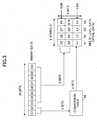
- FIG. 3 is a diagram for explaining the method of converting the binary data into the multi-level data in the multi-level data conversion circuit 15.
- FIG. 3 shows a case where a 10-bit binary data is to be converted into a 4-symbol octal data.
- the multi-level data amounting to 1 symbol includes 3 bits, and 4 symbols are regarded as 1 set, so as to treat the multi-level data in units of 4 symbols (S1 to S4).
- MSB indicates the most significant bit
- LSB indicates the least significant bit.
- 2 bits D1 and D2 of a 10-bit binary data are converted into 4 bits (L1 to L4) by a conversion table 34, and arranged in the LSB of the multi-level data. Remaining 8 bits (D3 to D10) of the 10-bit binary data are arranged in the MSB side of the multi-level data as shown in FIG. 3.
- the conversion table 34 may be provided within the multi-level data conversion circuit 15, for example.
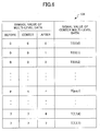
- FIG. 4 is a diagram showing contents of the conversion table 34 shown in FIG. 3.
- FIG. 4 shows 4 kinds (1) through (4) of the conversion table 34 which converts a 2-bit binary data (D1, D2) into a 4-bit data (L1 to L4).
- D1, D2 binary data
- L1 to L4 4-bit data
- an error at the time of the reproduction is approximately within ⁇ 1.
- the value 5 may be erroneously reproduced as the value 4 or 6, but it is very rare for the value 5 to be erroneously reproduced as the value 3 or 7.
- the tendency is for the LSB to become inverted such that 1 erroneously becomes 0 or vice versa.
- the LSB (L1 to L4) of each symbol within 1 set changes at random, and 16 kinds of bit patterns are possible. But by restricting the possible patterns of the LSB (L1 to L4) to 4 kinds for each of the 4 kinds (1) through (4) of the conversion table 34 shown in FIG. 4, it becomes possible to reduce the number of candidates to 1/4 at the time of judging the multi-level data and accordingly improve the accuracy of judging the multi-level data.
- the method of converting the 2-bit data into the 4-bit data may not be limited to 1 kind, and 2 kinds of methods may be switched and selectively used for every set.
- the numerical value series P may be made up of random numbers which are prescribed by an initial value and a generation method thereof.
- the judgement may be made not only based on the target set but based also on a plurality of sets before and after the target set, to thereby reduce the error.
- test data which is recorded on the optical disk 3 for use by a first multi-level data judging method, separately from the multi-level data.
- the test data is as follows in a case where 3 symbols of the octal data are consecutive.
- Test Data 000 001 002 003 004 005 006 007 010 011 012 013 014 015 016 017 020 021 022 023 024 025 026 027 ... ... 760 761 762 763 764 765 766 767 770 771 772 773 774 775 776 777
- the test data may be recorded on the optical disk 3 at a recording position in an inner peripheral portion, an outer peripheral portion and an intermediate portion of the optical disk 3. Alternatively, the test data may be recorded for every 1 revolution of the optical disk 3. The test data may also be inserted between the data which is obtained by converting the binary data into the multi-level data, for every predetermined period. By recording the test data on the optical disk 3, it is possible to suppress a change in the reproduced signal at the recording position on the optical disk 3, and stably reproduce the multi-level data.
- the method of judging the multi-level data carries out the following. That is, a reproduced signal of the test data is input, and signal values of the multi-level data are stored. A reproduced signal of the multi-level data which is obtained by converting the binary data is input, and errors between the signal values of the multi-level data and the stored signal values are calculated.
- the multi-level data having a smallest error as a judging candidate of each symbol within the set is regarded as a first candidate, and the multi-level data having the next smallest error is regarded as a second candidate.
- a candidate of a multi-level data series of m symbols within the set is generated using the first and second candidates of each symbol, according to the predetermined conversion rule which is used to convert the (m-k)-bit binary data into m bits.
- An error between the signal value of each symbol and stored signal value corresponding to the candidate multi-level data is calculated, and the multi-level data series having a smallest total error amounting to m symbols of 1 candidate is output as the reproduced multi-level data.
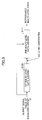
- FIG. 5 is a flow chart for explaining the multi-level data judging method employed by the multi-level data judging circuit 29 shown in FIG. 2.
- a step S109 carries out the first multi-level data judging process with respect to the output signal value of the waveform equalizer circuit 27 shown in FIG. 2. More particularly, the test data is reproduced, and a table 134 shown in FIG. 6 is created.
- FIG. 6 is a diagram showing this table 134 which stores signal values of a center multi-level data of all combinations of multi-level data of 3 consecutive symbols of the test data, that is, the output signal values of the waveform equalizer circuit 27.
- the value obtained by reproducing the test data once may be used as the signal value or, an average value of the values obtained by reproducing the test data a plurality of times may be used as the signal value.
- the table 134 shown in FIG. 6 may be provided within the multi-level data judging circuit 19, for example.
- the multi-level data is judged. More particularly, the signal values of the multi-level data of 3 consecutive symbols, that is, the output signal values of the waveform equalizer circuit 27 shown in FIG. 2, are input, and the symbol value of the center multi-level data is output. In order to do so, a provisional judgement is first made with respect to the multi-level data 1 symbol before and 1 symbol after. A threshold value which is used to make the provisional judgement is calculated from the values stored in the table 134 shown in FIG. 6.
- X(u) ⁇ L(u) + L(u+1) ⁇ /2
- the signal values of the multi-level data 1 symbol before and 1 symbol after are compared with the threshold value X(u) calculated from the formula (2), to provisionally judge the multi-level data 1 symbol before and 1 symbol after. More particularly, if the signal values of the multi-level data 1 symbol before and 1 symbol after are denoted by Y, v satisfying the following relationship (3) is regarded as the symbol value obtained by the provisional judgement.
- the symbol value q corresponding to the smallest error is output as a first candidate (q1)
- the symbol value q corresponding to the next smallest (second smallest) error is output as a second candidate (q2).
- the first and second candidates (q1 and q2) are output with respect to each symbol within 1 set.
- a step S111 inputs the first and second candidates of each symbol output by the step S109, and outputs the reproduced multi-level data by making a final judgement.
- FIG. 7A is a diagram showing the first and second candidates (q1 and q2) of each symbol within 1 set
- FIG. 7B is a diagram showing judging candidates amounting to 4 symbols within 1 set that are generated using the first and second candidates (q1 and q2) of each symbol based on the kind (1) of the conversion table 34 shown in FIG. 4.
- FIG. 7B also shows the contents of the kind (1) of the conversion table 34 shown in FIG. 4.
- L1 to L4 in the kind (1) of the conversion table 34 indicate only the LSB of the multi-level data, and indicate whether the multi-level data is an even number of an odd number. Accordingly, "0" in the conversion table 34 indicates an even number, and "1" indicates an odd number.
- first and second candidates (q1 and q2) of each symbol one is an even number and the other is an odd number.
- 4 kinds of judging candidates, each amounting to 4 symbols within 1 set, are generated by selecting the odd or even number candidate according to the conversion table 34.
- the final judgement result is output based on the 4 kinds of judging candidates.
- the error between the signal value of each symbol (output signal value of the waveform equalizer circuit 27) and the signal value corresponding to the symbol value of each judging candidate is obtained for 4 symbols and added, and the judging candidate which makes the total error for the 4 symbols the smallest is output as the final judgement result.
- the second multi-level data judging process generates the judging candidate within 1 set according to the conversion table 34, by using the first and second candidates (q1 and q2) of each symbol determined by the first multi-level data judging process. For this reason, the reliability of the judgement result is improved. Furthermore, since the redundant bit is increased to 2 bits, the number of judging candidates is reduced to 1/4 compared to the previously proposed multi-level data judging method described before in conjunction with FIG. 1, to thereby reduce erroneous judging of the multi-level data.
- the final judgement result is output using the data within 1 set.
- the predetermined conversion rule also uses the data within the previous set
- the multi-level data is judged using the data within a plurality of sets, as will be described hereunder.
- the candidate which makes the error the smallest is selected for the case where the numerical value series P is "0" and for the case where the numerical value series P is "1". Then, the candidate is selected in the following set which is related by the numerical value series P, for a case where the numerical value series P is "0” and for a case where the numerical value series P is "1" in a first set of the plurality of sets, so as to create the candidates amounting to the plurality of sets for 2 systems. Of the 2 systems of candidates, the candidate which makes the error smaller is output as the final judgement result.
- the judgement can be made not only based on the target set but also based on the plurality of sets including the target set, and the error can be reduced.
- the candidate which makes the error the second smallest or, all of the candidates may be used in each set.
- the candidate which makes the error the smallest of all combinations of the candidates in the plurality of sets may be output as the final judgement result.
- the multi-level data processing method described above may be realized by a software (computer program) which operates in a computer system having a microprocessor (or CPU), a digital signal processor or the like.
- the multi-level data processing method described above may be realized by an exclusive hardware. A description will now be given of a case where the multi-level data processing method is realized by the exclusive hardware.
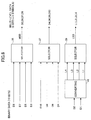
- FIG. 8 is a system block diagram showing a structure of the multi-level data conversion circuit 15 for converting the binary data into the multi-level data.
- FIG. 8 shows the multi-level data conversion circuit 15 which converts the 10-bit binary data into the 4-symbol octal data (3 bits).
- the multi-level data conversion circuit 15 shown in FIG. 8 includes 3 selectors 35, 37 and 39, and a converting circuit 41. Each of the selectors 35, 37 and 39 inputs a 4-bit data, and outputs 1 bit of the 4-bit data.
- the converting circuit 41 converts a 2-bit data into a 4-bit data. Hence, 10 bits are input in parallel to the multi-level data conversion circuit 15, and the multi-level data conversion circuit 15 outputs a parallel data indicating 1 symbol in 3 bits.
- the multi-level data conversion circuit 15 further includes a control circuit for generating control signals which control the switching of the selectors 35, 37 and 39 in synchronism with the timings of the input and output data, but the illustration thereof will be omitted for the sake of convenience.
- the functions of this control circuit may be realized by the microprocessor (or CPU) which controls the operation of the entire optical disk drive 1 shown in FIG. 2.
- the converting circuit 41 can realize the conversion table 34 by using known semiconductor memories and logic circuits.
- the selectors 35, 37 and 39 are controlled by the control circuit to successively output (D3, D4, L1), (D5, D6, L2), (D7, D8, L3) and (D9, D10, L4).
- the binary data can be converted into the multi-level data by the multi-level data conversion circuit 15 having a simple hardware structure.
- a switching circuit (not shown) may be switched to selectively output the test data and the multi-level data which is output from the circuit shown in FIG. 8 which converts the binary data into the multi-level data. In this case, it is possible to mix the test data and the multi-level data forming the user data.
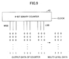
- FIG. 9 is a diagram showing a structure of a test data generating circuit.
- the test data generating circuit shown in FIG. 9 includes a 9-bit binary counter 43.
- an output of the 9-bit binary counter 43 is grouped into 3 3-bit portions, and each 3-bit portion is output as the multi-level data (octal data) so as to generate the test data shown on the right side of the 3 3-bit portions in FIG. 9.
- FIG. 10 is a functional block diagram showing a structure of the multi-level data judging circuit 29 shown in FIG. 2.
- the multi-level data judging circuit 29 includes a first multi-level data judging circuit 45 which realizes the first multi-level data judging method, and a second multi-level data judging circuit 47 which realizes the second multi-level data judging method.
- the first multi-level data judging circuit 45 outputs the first and second candidates (q1 and q2) of the judging candidate of each symbol, based on the output signal value of the waveform equalizer circuit 27.
- the second multi-level data judging circuit 47 carries out the final judgement based on the output signal value of the waveform equalizer circuit 27 and the first and second candidates (q1 and q2) output from the first multi-level data judging circuit 45, and outputs the reproduced multi-level data.
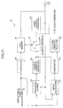
- FIG. 11 is a system block diagram showing a structure of the first multi-level data judging circuit 45.
- the first multi-level data judging circuit 45 includes an averaging circuit 49, a table memory circuit 51, a provisional judging circuit 53, a judging candidate generating circuit 55, an address switching circuit 57, a table address generating circuit 59, an error calculating circuit 61, a comparator circuit 63, and a first and second candidate selecting circuit 65.
- the averaging circuit 49 obtains an average value of the signal values output from the waveform equalizer circuit 27.
- the table memory circuit 51 forms the table 134 shown in FIG. 6.
- the table memory circuit 51 includes a data input terminal which receives the signal value when creating the table 134, a data output terminal which outputs the signal value when calculating the error, and an address input terminal which is used to input the value of a plurality of multi-level data. For example, when using 3 octal data to create a continuous table 134, a 9-bit address data is used in groups of 3-bit portions.
- the table memory circuit 51 also outputs the signal value to the second multi-level data judging circuit 47 shown in FIG. 12 which will be described later.
- the provisional judging circuit 53 determines the threshold value X(u) by calculating the formulas (1) and (2) described above using adders and the like, and further calculates the relationship (3) described above using comparators and the like, so as to provisionally judge the first and third multi-level data respectively before and after (on both sides of) the second (center) multi-level data of the 3 consecutive multi-level data.
- the judging candidate generating circuit 55 outputs the symbol values of the first and third multi-level data of the 3 consecutive multi-level data output from the provisional judging circuit 53, and the symbol value (0 to 7) of the candidate of the center multi-level data.
- the address switching circuit 57 switches the address data input to the address input terminal of the table memory circuit 51.
- the address switching circuit 57 inputs the output of the table address generating circuit 59 to the address input terminal of the table memory circuit 51.
- the address switching circuit 57 inputs the output of the judging candidate generating circuit 55 to the address input terminal of the table memory circuit 51.
- the address switching circuit 57 also has a switching function to output from the table 134 the signal value of the judging candidate to be used by a judging candidate output circuit 67 of the second multi-level data judging circuit 47 shown in FIG. 12 which will be described later.
- the test data is reproduced from the optical disk 3, and the signal value of the center multi-level data of all combinations of the multi-level data of 3 consecutive symbols is input to the table memory circuit 51.
- the symbol value of the multi-level data in this case is known as the test data, and can be generated by the test data generating circuit shown in FIG. 9.
- the table address generating circuit 59 is provided to input the test data which is output from the test data generating circuit shown in FIG. 9 as the multi-level data to the address input terminal of the table memory circuit 51.
- the table address generating circuit 59 also generates an address which is used when calculating the threshold value X(u) used for making the provisional judgement.
- the error calculating circuit 61 calculates an error between the signal values of the 8 candidates in the table 134 and the signal value of the center multi-level data which is input to the error calculating circuit 61.
- the comparator circuit 63 compares the errors output from the error calculating circuit 61 and rearranges the errors in an order of size starting from the smallest error.
- the first and second candidate selecting circuit 65 outputs the candidate (first candidate) which makes the error the smallest, and the candidate (second candidate) which makes the error the second smallest.
- the first multi-level data judging circuit 45 may further include a control circuit which controls the first multi-level data judging circuit 45 and the operation of the entire optical disk drive 1 shown in FIG. 2, but the illustration thereof will be omitted for the sake of convenience.
- the functions of this control circuit may be realized by the microprocessor (or CPU) which controls the operation of the entire optical disk drive 1.
- the test data recorded on the optical disk 3 is reproduced, and the signal value of the center multi-level data of the multi-level data of 3 consecutive symbols is input to the table memory circuit 51 by the operations of the table address generating circuit 59 and the averaging circuit 49, so as to create the table 134.
- the signal value in the table 134 is input to the provisional judging circuit 53, so as to calculate the threshold value X(u) for use in making the provisional judgement.
- the multi-level data which is obtained by converting the binary data and recorded on the optical disk 3 is reproduced from the optical disk 3.
- the signal values of the first and third multi-level data 1 symbol before and 1 symbol after the center multi-level data are obtained and input to the provisional judging circuit 53.
- the judging candidate generating circuit 55 Based on the provisional judgement result, the judging candidate generating circuit 55 outputs 8 kinds of judging candidates.
- the error calculating circuit 61 calculates the error between the signal value of the center multi-level data of the multi-level data of 3 consecutive data and the signal values in the table 134 corresponding to the 8 kinds of judging candidates.
- the comparator circuit 63 rearranges the order of the errors calculated by the error calculating circuit 61 in the order of size starting from the smallest error.
- the first and second candidate selecting circuit 65 outputs the judging candidate corresponding to the smallest error as the first candidate, and outputs the judging candidate corresponding to the second smallest error as the second candidate.
- FIG. 12 is a system block diagram showing a structure of the second multi-level data judging circuit 47.
- the second multi-level data judging circuit 47 includes the candidate signal value output circuit 67, an error calculating circuit 69, a first register circuit 71, a first selector circuit 73, an adder circuit 75, a second register circuit 77, a minimum value detecting circuit 79, a third register circuit 81, a second selector circuit 83, a control circuit 85, a conversion table 87, and a P generating circuit 89 which generates a numerical value series (P) for conversion table selection.
- P numerical value series
- the candidate signal value output circuit 67 outputs signal values corresponding to the symbol values of the first and second candidates of each symbol received from the first and second candidate selecting circuit 65 within the first multi-level data judging circuit 45 shown in FIG. 11.
- the values stored in the table memory circuit 51 within the first multi-level data judging circuit 45 are used for the signal values corresponding to the symbol values of the first and second candidates. Accordingly, the symbol values of the first and second candidates received from the first and second candidate selecting circuit 65 are output from the candidate signal value output circuit 67 and input to the address input terminal of the table memory circuit 51 via the address switching circuit 57.
- the signal values stored in the table 134 of the table memory circuit 51 are input to the candidate signal value output circuit 67 of the second multi-level data judging circuit 47, and then input to the error calculating circuit 69.
- the symbol values of the first and second candidates for each symbol are output from the candidate signal value output circuit 67 to the third register circuit 81.
- the error calculating circuit 69 calculates an error between the input signal value and the signal value of the judging candidate.
- the first register circuit 71 holds errors output from the error calculating circuit 69 and amounting to 1 set or, corresponding to a number of symbols amounting to a plurality of sets.
- the first selector circuit 73 selects an output of the first register circuit 71 in correspondence with a bit pattern of the conversion table 87, and outputs the selected output in order to calculate a total of the errors within 1 set or within the plurality of sets.
- the adder circuit 75 adds the errors output from the first selector circuit 73, and outputs a total value.
- the second register circuit 77 holds an output of the adder circuit 75.
- the minimum value detecting circuit 79 detects a minimum value from outputs of the second register circuit 77.
- the third register circuit 81 holds a symbol value series of the judging candidate amounting to 1 set or the plurality of sets received from the candidate signal value output circuit 67.
- the second selector circuit 83 selects a symbol value of the judging candidate held in the third register circuit 81 corresponding to the minimum value detected by the minimum value detecting circuit 79, in correspondence with the bit pattern of the conversion table 87, and outputs the selected symbol value as the judgement result.
- the control circuit 85 controls the operation of the entire second multi-level data judging circuit 47.
- the conversion table 87 is the same as the conversion table 34 described above for converting the binary data into the multi-level data.
- the P generating circuit 89 generates the numerical value series P which is used to select the conversion table 87 when switching the conversion table 87 for each set.
- the P generating circuit 89 may be omitted if only one kind of conversion table 87 is used.
- measures are taken so that the numerical value series P is the same as that used when converting the binary data into the multi-level data.
- the numerical value series P may be generated in the P generating circuit 89 by inputting the symbol value of the judging candidate.
- the second multi-level data judging circuit 47 shown in FIG. 12 the signal values corresponding to the first and second candidates of each symbol received from the first and second candidate selecting circuit 65 of the first multi-level data judging circuit 45 shown in FIG. 11 are output from the candidate signal value output circuit 67 shown in FIG. 12.
- the error calculating circuit 69 calculates the error of the signal values of the first and second candidates of each symbol with respect to the input signal value which is received from the waveform equalizer circuit 27 shown in FIG. 2.
- the symbol values of the first and second candidates of each symbol are held in the third register circuit 81.
- the first register circuit 71 holds the errors of the number of symbols corresponding to 1 set or the plurality of sets. Thereafter, the first selector circuit 73 selects and outputs to the adder circuit 75 the error of the signal values of all judging candidates based on the conversion table 87. Hence, the total of the errors for each judging candidate is calculated and held in the second register circuit 77. Then, the minimum value detecting circuit 79 detects the minimum value of the totals of the errors output from the second register circuit 79. Of the symbol values of the judging candidates held in the third register circuit 81, each symbol value corresponding to the judging candidate which makes the error the minimum value is selected by the second selector circuit 83, and output as the reproduced multi-level data.
- the second multi-level data judging circuit 47 shown in FIG. 12 can hold the errors for all combinations, amounting to the plurality of sets, of the judging candidates in each of the plurality of sets. For this reason, it is possible to select the candidate which makes the error the minimum not only from the combination of the candidates which make the error the minimum in each set, but also from all combination of the candidates.
- the multi-level data judging circuit 29 shown in FIG. 2 may be formed by the first multi-level data judging circuit 45 and the second multi-level data judging circuit 47 described above. Furthermore, by providing the multi-level data conversion circuit 15 and the multi-level data judging circuit 29 in the optical disk drive 1 shown in FIG. 2, it becomes possible to record information on and reproduce information from the optical disk 3.
- the analog-to-digital conversion of the ADC circuit 23 which quantizes the amplitude of the reproduced signal is employed as a means of quantizing the multi-level data signal.
- the means of quantizing the multi-level data signal is not limited to such, as will be described hereunder.
- FIG. 13 is a diagram for explaining a multi-level recording by varying lengths of the marks recorded on the information recording medium.
- the information recording medium is the optical disk 3 shown in FIG. 2.
- the reproduced signal is a binary data, but a change in the time lengths (durations) of pulses corresponding to the marks becomes a multi-level data (multi-level data signal).
- a counter circuit not shown which operates in response to a reference clock, it is possible to obtain a signal value (digital data) obtained by quantizing the multi-level data signal. Thereafter, a constant value may be subtracted from each signal value, so as to adapt the embodiment described above which employs the analog-to-digital conversion to the case shown in FIG. 13.
Landscapes
- Engineering & Computer Science (AREA)
- Signal Processing (AREA)
- Signal Processing For Digital Recording And Reproducing (AREA)
- Optical Recording Or Reproduction (AREA)
Applications Claiming Priority (2)
| Application Number | Priority Date | Filing Date | Title |
|---|---|---|---|
| JP2002316826A JP4027778B2 (ja) | 2002-10-30 | 2002-10-30 | 多値データ処理方法及び装置 |
| JP2002316826 | 2002-10-30 |
Publications (1)
| Publication Number | Publication Date |
|---|---|
| EP1416640A2 true EP1416640A2 (de) | 2004-05-06 |
Family
ID=32089558
Family Applications (1)
| Application Number | Title | Priority Date | Filing Date |
|---|---|---|---|
| EP20030256482 Withdrawn EP1416640A2 (de) | 2002-10-30 | 2003-10-15 | Mehrpegeldatenverarbeitungsverfahren und -gerät |
Country Status (5)
| Country | Link |
|---|---|
| US (1) | US7251207B2 (de) |
| EP (1) | EP1416640A2 (de) |
| JP (1) | JP4027778B2 (de) |
| CN (1) | CN100337406C (de) |
| TW (1) | TWI236615B (de) |
Families Citing this family (10)
| Publication number | Priority date | Publication date | Assignee | Title |
|---|---|---|---|---|
| JP2005259306A (ja) * | 2004-03-15 | 2005-09-22 | Ricoh Co Ltd | 情報記録方法、情報記録装置、及び情報記録媒体 |
| JP2005267674A (ja) * | 2004-03-16 | 2005-09-29 | Ricoh Co Ltd | 情報記録方法と情報記録装置 |
| JP4446348B2 (ja) * | 2004-03-18 | 2010-04-07 | 株式会社リコー | 情報記録方法及び情報記録装置 |
| JP2005339678A (ja) * | 2004-05-27 | 2005-12-08 | Ricoh Co Ltd | 情報記録方法、情報再生方法、情報記録装置及び情報再生装置 |
| US7599272B2 (en) * | 2004-11-22 | 2009-10-06 | Canon Kabushiki Kaisha | Method and apparatus for recording and reproducing multi-level information |
| US7786904B1 (en) * | 2008-11-05 | 2010-08-31 | Mingchih Hsieh | Voltage level digital system |
| US8345526B2 (en) * | 2010-12-29 | 2013-01-01 | General Electric Company | Non-binary holograms for increased capacity |
| JP6179401B2 (ja) | 2011-03-09 | 2017-08-16 | 横浜ゴム株式会社 | タイヤ/ホイール組立体 |
| JP6774512B2 (ja) * | 2019-01-23 | 2020-10-28 | アンリツ株式会社 | Fecエラー付加装置、それを用いた試験信号発生装置、及びfecエラー付加方法 |
| CN113870921B (zh) * | 2021-12-02 | 2022-03-18 | 之江实验室 | 一种忆阻器阵列上符号数映射方法 |
Family Cites Families (25)
| Publication number | Priority date | Publication date | Assignee | Title |
|---|---|---|---|---|
| FR2128131B1 (de) * | 1971-03-05 | 1975-02-21 | Lignes Telegraph Telephon | |
| US3831145A (en) * | 1973-07-20 | 1974-08-20 | Bell Telephone Labor Inc | Multilevel data transmission systems |
| US4118791A (en) * | 1977-04-25 | 1978-10-03 | Norlin Music, Inc. | Multi-level encoding system |
| US4408189A (en) * | 1981-05-18 | 1983-10-04 | Northern Telecom Limited | Method and apparatus for code conversion of binary to multilevel signals |
| US5142380A (en) * | 1989-10-23 | 1992-08-25 | Ricoh Company, Ltd. | Image data processing apparatus |
| JPH03142717A (ja) * | 1989-10-27 | 1991-06-18 | Ricoh Co Ltd | 光ディスク |
| US5344683A (en) * | 1989-10-27 | 1994-09-06 | Ricoh Company, Ltd. | Optical information recording medium with phase grooves in land portions of information recording areas |
| US5497194A (en) * | 1990-01-11 | 1996-03-05 | Ricoh Company, Ltd. | Electronic camera for photographing and recording an image and for recording and reproducing a voice |
| JPH04107013A (ja) * | 1990-08-28 | 1992-04-08 | Ricoh Co Ltd | 可変長符号の符号化回路 |
| US5638354A (en) * | 1993-07-16 | 1997-06-10 | Ricoh Company, Ltd. | Optical information recording medium |
| US5537382A (en) * | 1994-11-22 | 1996-07-16 | Optex Corporation | Partial response coding for a multi-level optical recording channel |
| JP3065529B2 (ja) * | 1996-03-12 | 2000-07-17 | 株式会社リコー | 光情報記録媒体および光情報記録媒体のトラッキングサーボ方法 |
| US6005895A (en) * | 1996-12-20 | 1999-12-21 | Rambus Inc. | Apparatus and method for multilevel signaling |
| US7239602B2 (en) * | 1998-08-27 | 2007-07-03 | Ricoh Company, Ltd. | Optical information recording medium with a partition wall between an information tracks groove and a preformat pit encoding information therefor |
| JP3209948B2 (ja) * | 1997-08-27 | 2001-09-17 | 株式会社リコー | 光情報記録媒体及びその原盤露光方法 |
| JPH11296918A (ja) * | 1998-04-08 | 1999-10-29 | Ricoh Co Ltd | 光情報記録媒体用スタンパの製造方法 |
| US6487149B1 (en) * | 1998-10-09 | 2002-11-26 | Ricoh Company, Ltd. | Optical recording and reproducing methods for optical disk |
| JP4759794B2 (ja) | 2000-04-26 | 2011-08-31 | 株式会社三洋物産 | 遊技機 |
| US6987720B2 (en) * | 2000-07-13 | 2006-01-17 | Ricoh Company, Ltd. | Information recording and/or reproducing apparatus, information recording and/or reproducing method, and phase-change recording medium for use in the apparatus and the methods |
| JP3969958B2 (ja) * | 2001-02-14 | 2007-09-05 | 株式会社リコー | 光情報記録方法 |
| US7082091B2 (en) * | 2001-07-31 | 2006-07-25 | Ricoh Company, Ltd. | Information reproducing method judging a multivalued level of a present cell by referring to judged multivalued levels of a preceding cell and an ensuing cell |
| EP1296457B1 (de) * | 2001-09-21 | 2009-04-29 | Ricoh Company, Ltd. | Multi-Level Datenverarbeitung für die Aufzeichnung |
| JP4209694B2 (ja) * | 2002-03-08 | 2009-01-14 | 株式会社リコー | テストデータ記録方法とプログラム |
| TWI255452B (en) * | 2002-03-18 | 2006-05-21 | Ricoh Kk | Multi-level information recording apparatus, multi-level information recording method, multi-level information recording medium and multi-level information recording-reproducing apparatus |
| US7046610B2 (en) * | 2002-04-24 | 2006-05-16 | Ricoh Company, Ltd. | Recording medium suitable for recording/reproducing multi-level data |
-
2002
- 2002-10-30 JP JP2002316826A patent/JP4027778B2/ja not_active Expired - Fee Related
-
2003
- 2003-10-13 TW TW092128320A patent/TWI236615B/zh not_active IP Right Cessation
- 2003-10-15 EP EP20030256482 patent/EP1416640A2/de not_active Withdrawn
- 2003-10-21 US US10/689,029 patent/US7251207B2/en not_active Expired - Fee Related
- 2003-10-30 CN CNB2003101222858A patent/CN100337406C/zh not_active Expired - Fee Related
Also Published As
| Publication number | Publication date |
|---|---|
| TWI236615B (en) | 2005-07-21 |
| US20040085878A1 (en) | 2004-05-06 |
| CN1519842A (zh) | 2004-08-11 |
| TW200416591A (en) | 2004-09-01 |
| US7251207B2 (en) | 2007-07-31 |
| JP4027778B2 (ja) | 2007-12-26 |
| CN100337406C (zh) | 2007-09-12 |
| JP2004152416A (ja) | 2004-05-27 |
Similar Documents
| Publication | Publication Date | Title |
|---|---|---|
| US6888479B2 (en) | Data processing method, circuit, and apparatus with increased accuracy | |
| US5506827A (en) | Digital data reproducing apparatus | |
| JPH07220409A (ja) | ディジタル信号再生装置 | |
| US7251207B2 (en) | Multi-level data processing method and apparatus | |
| US5424882A (en) | Signal processor for discriminating recording data | |
| US7190653B2 (en) | Data recording/reproducing device | |
| JP3572047B2 (ja) | 光ディスク装置と光ディスク再生方法 | |
| US6532337B1 (en) | Digital-signal playback apparatus | |
| JP4589977B2 (ja) | データ処理回路とデータ処理装置 | |
| US6731699B2 (en) | Detector, reproduction system, receiver and method | |
| US6369724B1 (en) | Modulating apparatus and method, demodulating apparatus and method, and transmission medium | |
| EP0903864B1 (de) | Demodulator und Demodulationsverfahren | |
| US6704259B2 (en) | Information recording and reproducing apparatus and information recording and reproducing method, information reproducing apparatus and information reproducing method, and information recording medium | |
| JP3810703B2 (ja) | データ処理方法とデータ処理回路とデータ処理装置 | |
| JP4137138B2 (ja) | データ処理方法 | |
| JP3810690B2 (ja) | 多値データ処理方法と多値データ処理装置 | |
| KR100535292B1 (ko) | 데이타전송장치및데이타전송방법 | |
| JP4027774B2 (ja) | 情報記録装置及び情報再生装置 | |
| JP4303090B2 (ja) | 多値データ変換処理方法と多値データ変換処理装置 | |
| JP4383246B2 (ja) | 情報記録方法及び情報記録装置 | |
| JP2004272979A (ja) | 多値データ信号の直流成分制御方法と直流成分制御装置 | |
| JP2004079039A (ja) | 復号方法及び復号装置 |
Legal Events
| Date | Code | Title | Description |
|---|---|---|---|
| PUAI | Public reference made under article 153(3) epc to a published international application that has entered the european phase |
Free format text: ORIGINAL CODE: 0009012 |
|
| 17P | Request for examination filed |
Effective date: 20031105 |
|
| AK | Designated contracting states |
Kind code of ref document: A2 Designated state(s): AT BE BG CH CY CZ DE DK EE ES FI FR GB GR HU IE IT LI LU MC NL PT RO SE SI SK TR |
|
| AX | Request for extension of the european patent |
Extension state: AL LT LV MK |
|
| RAP1 | Party data changed (applicant data changed or rights of an application transferred) |
Owner name: RICOH COMPANY LTD. |
|
| STAA | Information on the status of an ep patent application or granted ep patent |
Free format text: STATUS: THE APPLICATION HAS BEEN WITHDRAWN |
|
| 18W | Application withdrawn |
Effective date: 20090602 |