EP1416460A1 - Appareil d'affichage du type matriciel - Google Patents
Appareil d'affichage du type matriciel Download PDFInfo
- Publication number
- EP1416460A1 EP1416460A1 EP20020717167 EP02717167A EP1416460A1 EP 1416460 A1 EP1416460 A1 EP 1416460A1 EP 20020717167 EP20020717167 EP 20020717167 EP 02717167 A EP02717167 A EP 02717167A EP 1416460 A1 EP1416460 A1 EP 1416460A1
- Authority
- EP
- European Patent Office
- Prior art keywords
- wirings
- main surface
- substrate
- back side
- scanning line
- Prior art date
- Legal status (The legal status is an assumption and is not a legal conclusion. Google has not performed a legal analysis and makes no representation as to the accuracy of the status listed.)
- Withdrawn
Links
- 239000011159 matrix material Substances 0.000 title claims description 57
- 239000000758 substrate Substances 0.000 claims description 92
- 239000000463 material Substances 0.000 claims description 51
- 239000010409 thin film Substances 0.000 claims description 19
- 238000010894 electron beam technology Methods 0.000 claims description 15
- 239000011888 foil Substances 0.000 claims description 5
- 239000012780 transparent material Substances 0.000 claims description 4
- 230000005684 electric field Effects 0.000 claims description 3
- 239000002184 metal Substances 0.000 claims 8
- 239000010410 layer Substances 0.000 description 26
- 238000005401 electroluminescence Methods 0.000 description 14
- 239000010408 film Substances 0.000 description 14
- 239000011521 glass Substances 0.000 description 13
- RYGMFSIKBFXOCR-UHFFFAOYSA-N Copper Chemical compound [Cu] RYGMFSIKBFXOCR-UHFFFAOYSA-N 0.000 description 10
- 229910052802 copper Inorganic materials 0.000 description 10
- 239000010949 copper Substances 0.000 description 10
- 238000000034 method Methods 0.000 description 10
- PXHVJJICTQNCMI-UHFFFAOYSA-N Nickel Chemical compound [Ni] PXHVJJICTQNCMI-UHFFFAOYSA-N 0.000 description 8
- 230000003446 memory effect Effects 0.000 description 8
- 229920006254 polymer film Polymers 0.000 description 7
- 239000003989 dielectric material Substances 0.000 description 5
- VYZAMTAEIAYCRO-UHFFFAOYSA-N Chromium Chemical compound [Cr] VYZAMTAEIAYCRO-UHFFFAOYSA-N 0.000 description 4
- 230000020169 heat generation Effects 0.000 description 4
- 238000004020 luminiscence type Methods 0.000 description 4
- 229910052759 nickel Inorganic materials 0.000 description 4
- 230000009467 reduction Effects 0.000 description 4
- 238000007789 sealing Methods 0.000 description 4
- 238000004544 sputter deposition Methods 0.000 description 4
- 230000008901 benefit Effects 0.000 description 3
- 238000009826 distribution Methods 0.000 description 3
- 238000005530 etching Methods 0.000 description 3
- 230000005284 excitation Effects 0.000 description 3
- 238000000059 patterning Methods 0.000 description 3
- 239000011295 pitch Substances 0.000 description 3
- 238000007639 printing Methods 0.000 description 3
- 239000000126 substance Substances 0.000 description 3
- OKTJSMMVPCPJKN-UHFFFAOYSA-N Carbon Chemical compound [C] OKTJSMMVPCPJKN-UHFFFAOYSA-N 0.000 description 2
- BQCADISMDOOEFD-UHFFFAOYSA-N Silver Chemical compound [Ag] BQCADISMDOOEFD-UHFFFAOYSA-N 0.000 description 2
- 239000002041 carbon nanotube Substances 0.000 description 2
- 229910021393 carbon nanotube Inorganic materials 0.000 description 2
- 230000000694 effects Effects 0.000 description 2
- 238000002474 experimental method Methods 0.000 description 2
- 239000011229 interlayer Substances 0.000 description 2
- 230000007257 malfunction Effects 0.000 description 2
- 239000011368 organic material Substances 0.000 description 2
- 238000005192 partition Methods 0.000 description 2
- 229920002120 photoresistant polymer Polymers 0.000 description 2
- 230000008569 process Effects 0.000 description 2
- 238000007650 screen-printing Methods 0.000 description 2
- 229910052709 silver Inorganic materials 0.000 description 2
- 239000004332 silver Substances 0.000 description 2
- 229910000679 solder Inorganic materials 0.000 description 2
- 230000002459 sustained effect Effects 0.000 description 2
- 229910000881 Cu alloy Inorganic materials 0.000 description 1
- 229910004205 SiNX Inorganic materials 0.000 description 1
- 239000004411 aluminium Substances 0.000 description 1
- XAGFODPZIPBFFR-UHFFFAOYSA-N aluminium Chemical compound [Al] XAGFODPZIPBFFR-UHFFFAOYSA-N 0.000 description 1
- 229910052782 aluminium Inorganic materials 0.000 description 1
- 230000003321 amplification Effects 0.000 description 1
- 239000003990 capacitor Substances 0.000 description 1
- 230000007797 corrosion Effects 0.000 description 1
- 238000005260 corrosion Methods 0.000 description 1
- 238000010586 diagram Methods 0.000 description 1
- 238000011156 evaluation Methods 0.000 description 1
- 230000006870 function Effects 0.000 description 1
- PCHJSUWPFVWCPO-UHFFFAOYSA-N gold Chemical compound [Au] PCHJSUWPFVWCPO-UHFFFAOYSA-N 0.000 description 1
- 229910052737 gold Inorganic materials 0.000 description 1
- 239000010931 gold Substances 0.000 description 1
- 238000009413 insulation Methods 0.000 description 1
- 238000004519 manufacturing process Methods 0.000 description 1
- 238000005259 measurement Methods 0.000 description 1
- 230000004048 modification Effects 0.000 description 1
- 238000012986 modification Methods 0.000 description 1
- 150000004767 nitrides Chemical class 0.000 description 1
- 238000003199 nucleic acid amplification method Methods 0.000 description 1
- 239000002245 particle Substances 0.000 description 1
- 230000002093 peripheral effect Effects 0.000 description 1
- 229920000642 polymer Polymers 0.000 description 1
- 238000012545 processing Methods 0.000 description 1
- 238000005215 recombination Methods 0.000 description 1
- 230000006798 recombination Effects 0.000 description 1
- 230000004044 response Effects 0.000 description 1
- 230000035939 shock Effects 0.000 description 1
- 125000006850 spacer group Chemical group 0.000 description 1
- 230000000007 visual effect Effects 0.000 description 1
Images


Classifications
-
- G—PHYSICS
- G09—EDUCATION; CRYPTOGRAPHY; DISPLAY; ADVERTISING; SEALS
- G09G—ARRANGEMENTS OR CIRCUITS FOR CONTROL OF INDICATING DEVICES USING STATIC MEANS TO PRESENT VARIABLE INFORMATION
- G09G3/00—Control arrangements or circuits, of interest only in connection with visual indicators other than cathode-ray tubes
- G09G3/20—Control arrangements or circuits, of interest only in connection with visual indicators other than cathode-ray tubes for presentation of an assembly of a number of characters, e.g. a page, by composing the assembly by combination of individual elements arranged in a matrix no fixed position being assigned to or needed to be assigned to the individual characters or partial characters
-
- G—PHYSICS
- G09—EDUCATION; CRYPTOGRAPHY; DISPLAY; ADVERTISING; SEALS
- G09F—DISPLAYING; ADVERTISING; SIGNS; LABELS OR NAME-PLATES; SEALS
- G09F9/00—Indicating arrangements for variable information in which the information is built-up on a support by selection or combination of individual elements
- G09F9/30—Indicating arrangements for variable information in which the information is built-up on a support by selection or combination of individual elements in which the desired character or characters are formed by combining individual elements
-
- H—ELECTRICITY
- H01—ELECTRIC ELEMENTS
- H01J—ELECTRIC DISCHARGE TUBES OR DISCHARGE LAMPS
- H01J31/00—Cathode ray tubes; Electron beam tubes
- H01J31/08—Cathode ray tubes; Electron beam tubes having a screen on or from which an image or pattern is formed, picked up, converted, or stored
- H01J31/10—Image or pattern display tubes, i.e. having electrical input and optical output; Flying-spot tubes for scanning purposes
- H01J31/12—Image or pattern display tubes, i.e. having electrical input and optical output; Flying-spot tubes for scanning purposes with luminescent screen
- H01J31/123—Flat display tubes
- H01J31/125—Flat display tubes provided with control means permitting the electron beam to reach selected parts of the screen, e.g. digital selection
- H01J31/127—Flat display tubes provided with control means permitting the electron beam to reach selected parts of the screen, e.g. digital selection using large area or array sources, i.e. essentially a source for each pixel group
-
- H—ELECTRICITY
- H10—SEMICONDUCTOR DEVICES; ELECTRIC SOLID-STATE DEVICES NOT OTHERWISE PROVIDED FOR
- H10K—ORGANIC ELECTRIC SOLID-STATE DEVICES
- H10K59/00—Integrated devices, or assemblies of multiple devices, comprising at least one organic light-emitting element covered by group H10K50/00
- H10K59/10—OLED displays
- H10K59/17—Passive-matrix OLED displays
- H10K59/179—Interconnections, e.g. wiring lines or terminals
-
- G—PHYSICS
- G09—EDUCATION; CRYPTOGRAPHY; DISPLAY; ADVERTISING; SEALS
- G09G—ARRANGEMENTS OR CIRCUITS FOR CONTROL OF INDICATING DEVICES USING STATIC MEANS TO PRESENT VARIABLE INFORMATION
- G09G2300/00—Aspects of the constitution of display devices
- G09G2300/04—Structural and physical details of display devices
- G09G2300/0421—Structural details of the set of electrodes
- G09G2300/0426—Layout of electrodes and connections
-
- G—PHYSICS
- G09—EDUCATION; CRYPTOGRAPHY; DISPLAY; ADVERTISING; SEALS
- G09G—ARRANGEMENTS OR CIRCUITS FOR CONTROL OF INDICATING DEVICES USING STATIC MEANS TO PRESENT VARIABLE INFORMATION
- G09G2320/00—Control of display operating conditions
- G09G2320/02—Improving the quality of display appearance
- G09G2320/0223—Compensation for problems related to R-C delay and attenuation in electrodes of matrix panels, e.g. in gate electrodes or on-substrate video signal electrodes
-
- H—ELECTRICITY
- H10—SEMICONDUCTOR DEVICES; ELECTRIC SOLID-STATE DEVICES NOT OTHERWISE PROVIDED FOR
- H10K—ORGANIC ELECTRIC SOLID-STATE DEVICES
- H10K59/00—Integrated devices, or assemblies of multiple devices, comprising at least one organic light-emitting element covered by group H10K50/00
- H10K59/80—Constructional details
- H10K59/87—Passivation; Containers; Encapsulations
Definitions
- the present invention relates to a matrix type display apparatus such as an electron beam excited luminescent material display apparatus using a flat electron source (SCE emitter), a plasma display panel, or an electroluminescence (EL) display apparatus which utilizes the electroluminescence phenomenon of a luminescent material, and more particularly to a matrix type display apparatus with an improved wiring structure.
- a matrix type display apparatus such as an electron beam excited luminescent material display apparatus using a flat electron source (SCE emitter), a plasma display panel, or an electroluminescence (EL) display apparatus which utilizes the electroluminescence phenomenon of a luminescent material, and more particularly to a matrix type display apparatus with an improved wiring structure.
- SCE emitter flat electron source
- EL electroluminescence
- a display mode of exciting a luminescent material by using an electron beam has been widely used as a television apparatus using a cathode ray tube as a high-quality picture video apparatus. That is because this display mode has a high response speed and a wide visual angle characteristic and is applied to a luminescent type display apparatus.
- a weight and a depth of the cathode ray tube are increased as a screen size becomes larger, and a 40-inch size is a limit in the prior art cathode ray tube. Therefore, 30-inch size or smaller cathode ray tube has been generally used for the domestic purpose.
- a picture signal of the NTSC type has been shifted to that of the high-vision type, and a display apparatus with a large screen is demanded with realization of higher quality.
- an electron beam excited luminescent material display apparatus using a planar electron source As a recent large-screen thin display, there is an electron beam excited luminescent material display apparatus using a planar electron source (E. Yamaguchi, et. al., "A 10-in. SCE-emitter display", Journal of SID, Vol. 5, p345, 1997).
- This electron beam excited luminescent material display apparatus has the following merits. That is, an electron emission element array as a planar electron source can be formed by using a printing technique. This is based on the same luminescence principle as that of the cathode ray tube because in the luminescent material exited light emission using electrons. Further, the planar electron source can be driven with a voltage of over 10 V, and a drive IC with a low withstand voltage can hence be used.
- an electron source which is of a so-called Spindt type, which sharpens the shape of an electron emission portion into a conical form and realizes the field concentration, an electron source using a carbon nanotube having a thickness in the order of nano-meters, and others, as well as the above-described planar electron source. Since the electrons subjected to field emission are accelerated with a high voltage of the kV order and the luminescent material is excited and caused to emit light, such electron sources have a characteristic capable of obtaining the same high quality as that of the cathode ray tube.
- a plasma display panel which can realize a large-screen panel with a low cost by forming wirings or pixels based on a printing mode has come into practical use. Since this PDP uses the ultraviolet rays generated by discharge for each pixel to cause the luminescent material formed on a panel surface to emit light in order to obtain an image, it displays a picture based on the image generation principle similar to that of the cathode ray tube in theory. The difference from the cathode ray tube lies in that the luminescent material is excited and caused to emit light by using ultraviolet rays. Furthermore, the gray scale display is generally controlled by the number of discharges, realized by applying a pulse voltage of approximately 200 V.
- an electroluminescence matrix type display apparatus utilizing the electroluminescence (EL) phenomenon of luminescent material, i.e. an LED matrix type display apparatus, which injects electrons and electron holes and emits light with the carrier recombination energy.
- EL electroluminescence
- a unimolecular or polymer organic material is used, and the material having the red, green and blue light emission characteristic is formed within the pixels, thereby enabling full-color display.
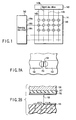
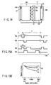
- FIG. 1 shows a basic structural example of a prior art matrix type display apparatus.
- Scanning line wirings 144 (144a, 144b, ...) and signal line wirings 145 (145a, 145b, ...) are formed on a display area 141, and pixels 146 are provided at intersections of these wirings.
- the scanning line wirings 144 supply a control pulse voltage of a scanning line driver circuit 142 to each pixel, and the signal line wirings 145 supply a display signal voltage from a signal line driver circuit 143 to each pixel.
- the structure of each pixel varies depending on the display mode of the display panel.
- FIGS. 2A and 2B are a plan view of an electron source constituted at a pixel of an electron beam excited luminescent material display panel using a field emission type planar electron source and a cross-sectional view of the display panel. Electrodes 151 and 152 and a conductive thin film 153 are formed on an insulating substrate 155, and an electron emission portion 154 is formed on a part of these members. Applying a voltage to the electron source from the electrodes 151 and 152 causes electron 159 to be emitted into a vacuum from the electron emission portion 154. The emitted electron flows into an anode electrode 156 formed on an opposed glass substrate 158.
- the electron passes through the anode electrode 156 and is injected into a luminescent material layer 157, thereby causing the luminescent material 157 to emit light. Since the quantity of electrons to be subjected to field emission can be controlled based on a voltage applied to the electrode 151 and 152 or a voltage application time, the luminescent brightness can be changed.
- FIG. 3 shows the structure in more detail. Electron sources 163 are connected to scanning line wirings 161 (161a, 161b, ...) and signal line wirings 162 (162a, 162b, ). Pixels 165 are provided at respective intersections of the scanning line wirings 161 and the signal line wirings 162, and an electron source 163 is formed for each pixel. Emission of electrons from an electron emission portion 164 of the electron source 163 is controlled by using a pulse voltage applied to the scanning line wirings 161 and the signal line wirings 162.
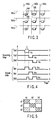
- FIG. 4 shows an actual voltage pulse application method for this type of display panel.
- Reference characters Va1, Va2, Va3 denote waveforms of voltages applied to the scanning line wirings and correspond to voltage waveforms of the first, second and third scanning line wirings, respectively.
- pulse application is again repeated from the first scanning line.
- Reference characters Vb1, Vb2, Vb3, ... designate pulse voltage waveforms of a display signal to be applied to the signal line wirings and correspond to voltage waveforms of the first, second and third signal line wirings, respectively.
- This pulse voltage is applied in synchronization with the scanning line pulse voltage, and its pulse width or voltage amplification value varies depending on the brightness. In this example, the brightness is controlled by using the pulse width.
- a voltage value of the pulse voltage to be applied to the signal line wirings is Vm, and a difference from the voltage value of the scanning line wirings is applied to the flat electron source.
- FIG. 5 shows a display state of the pixel corresponding to voltage application depicted in FIG. 4.
- the current driven type LED display apparatus or a field driven type electroluminescent display apparatus is also a two-terminal display element connected to the scanning line wirings and the signal line wirings and driven by the method shown in FIGS. 3 to 5 in theory even though it has a structure different from that of the basic pixels depicted in FIGS. 2A and 2B.
- the plasma display which causes the luminescent material to emit light by ultraviolet excitation based on plasma discharge adopts such a structure as shown in FIG. 6.
- a drive pulse is applied to scanning line wirings 194 (194a, 194b, ...) from a scanning line driver circuit 191, and a drive pulse is applied to signal line wirings 196 (196a, 196b, ...) from a signal line driver circuit 193.
- one discharge is completed by application of one voltage pulse, and discharge is not sustained, and hence a plurality of discharges must be generated in order to control the brightness.
- the pulse voltage sustains discharge for the number of pulse applications by the memory effect, thereby enabling brightness control.
- Wirings to sustain this discharge are 195 (165a, 165b, ...), and a voltage is supplied from a sustaining pulse driver circuit 192.
- Pixels 197 are defined at intersections of the scanning lines, the signal lines, and the sustaining voltage wirings. It is to be noted that reference numeral 198 in the drawing denotes a partition to avoid discharge due to malfunction of an adjacent pixel.
- FIG. 7 is a cross-sectional view showing a one-pixel portion structure of the plasma display.
- a scanning line wiring 202 and a sustaining pulse wiring 203 are formed on a glass substrate 201, and a dielectric film or the like is formed on the wirings, although not shown.
- a signal line wiring 206 is formed on an opposed substrate 205, and a luminescent material layer 207 is provided thereon.
- a signal voltage pulse is applied to the signal line wiring 206, and discharge 208 occurs if a difference in potential between the both electrodes is sufficiently high.
- the sustaining voltage pulse continues to be alternately applied to the sustaining pulse wiring 203 and to the scanning line wiring 202, thereby repeating the discharge 208. That is because the stored charge remains on the dielectric film on the electrodes 202 and 203 and provides the memory effect.
- Application of the reset pulse can eliminate the stored charge and reset the memory effect.
- each pulse width is ⁇ seconds or a shorter time because many discharges are produced within a limited scanning time.
- the driving method can display an arbitrary image including the gray scale in theory, by applying the drive pulse voltages to the scanning line wirings and the signal line wirings orthogonal to each other.
- Such a matrix type display panel has been developed/come into practical use as a thin/lightweight large display apparatus, replacing the conventional cathode ray tube type which cannot be increased in size because of its depth and weight.
- drive signals are applied to the respective pixels through the scanning line wirings and signal line wirings.
- the scanning line wirings in particular, since all pixels along the scanning line wirings are targets of the display operation when a selection pulse voltage is applied, and thus the load is large in view of the driver circuit. That is, in the field emission type electron beam excited fluorescent material display panel or the current driven type LED display panel, since a large current flows into the scanning lines, the voltage drops due to the wiring resistance.
- the signal waveform is distorted due to the load capacity and the wiring resistance.
- the voltage with a pulse width corresponding to a short time must be applied and the discharge current must be caused to flow, there occurs a problem of voltage drop due to an instantaneous large current besides the distortion of the voltage waveform.
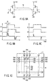
- the driver circuit In the mode shown in FIG. 8B, however, the driver circuit must be doubled, which results in an increase in cost. Further, a slight difference in timing of the right and left drive circuits or a difference in application voltage causes problems such as an increase in power consumption or heat generation of the driver LSI, which also affects the performance of the display panel.
- a current flows through right and left CMOS driver circuits in a period that the right and left pulse voltages deviate from each other in time, and the reactive power is basically consumed with respect to the operation using only the charging current.
- FIG. 9B shows a case that a time difference between gate voltages Vr and Vl of the CMOS circuits provided on the right and left sides of the panel is large, and an illustrated current Iw flows in a lag time of Vl relative to Vr, and the reactive power is generated in this period.
- FIG. 9C shows a case that a lag time of Vl relative to Vr is small.
- a matrix type display apparatus comprising:
- a matrix type luminescent material display apparatus comprising:
- a matrix type display apparatus comprising:
- a matrix type luminescent material display apparatus comprising:
- either scanning line wirings or signal line wirings, or both are connected with back side wirings formed on a back side of a substrate at both end portions of the substrate. Therefore, the voltage drop caused due to a wiring resistance of the scanning line wirings or the signal line wirings connected to the back side wirings can be reduced. Further, applying a drive pulse to the scanning line wirings or the like through the back side wirings can solve the problem of the brightness inclination generated by driving from one side. Furthermore, driving is enabled by one drive circuit, as compared with the structure providing drive circuits on both sides of the scanning line wirings, thereby avoiding an increase in cost and power consumption.
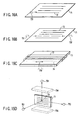
- FIGS. 10 to 13 are plan views showing a schematic structure of a matrix type display apparatus according to a first embodiment of the present invention.
- scanning line wirings 12 (12a 12b, 12c, ...) are formed in the horizontal direction and signal line wirings 14 (14a, 14b, 14c, ...) are formed in the vertical direction on an insulating substrate (array substrate) 11 made of a glass substrate. Electrode terminals for external connection 12a1, 12b1, 12c1, ..., 12a2, 12b2, 12c2, ..., 14a1, 14b1, 14c1, ..., 14a2, 14b2, 14c2, ... are formed at both ends of the respective wirings.
- the number of scanning line wirings is 480
- the number of signal line wirings is 640 ⁇ 3 ( ⁇ 3 corresponds to pixels R, G and B)
- wiring pitches are 900 ⁇ m and 300 ⁇ m, respectively.
- Pixels are defined at respective intersections of the scanning line wirings 12 and the signal line wirings 14, and a planar electron source 17 which acts as an electron emission element is provided at each pixel.
- a planar electron source 17 which acts as an electron emission element is provided at each pixel.
- the scanning line wirings 12 and the signal line wirings 14 are formed of an Ag paste by screen printing. Furthermore, both wirings are insulated from each other by an insulation layer formed by printing.
- a position indicated by a broken line 16 in FIG. 10 is a sealing region in which an array substrate (rear plate) 11 on which the electron sources 17 are formed is bonded to an opposed substrate (face plate) on which a luminescent material layer and an anode electrode are formed, and the rear plate and the face plate are sealed and connected by frit glass or the like after completion. At that time, the rear plate and the face plate are sealed with a gap of several mm.
- fluorescent substances which become red, green and blue at the luminescent wavelength peak are applied on the inner surface of the face plate, and a pattern of the face plate is formed with a pitch corresponding to each pixel on the rear plate. That is, the number of fluorescent substances for each of red light emission, green light emission and blue light emission is 480 in the scanning line direction and 640 in the signal line direction with a pitch of 900 ⁇ m.
- a thin-film type aluminium layer is formed on the luminescent material layer, an anode voltage Va to accelerate electrons is applied thereto in the display operation.
- an anode voltage Va to accelerate electrons is applied thereto in the display operation.
- the inside of the display cells is vacuum-pumped through an exhaust tube provided outside the display region.
- the inside of the sealing region indicated by the broken line 16 in FIG. 10 becomes a vacuum region.
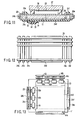
- FIG. 11 is a cross-sectional view of the display panel used in this embodiment in the scanning line direction, and on the glass substrate 11 are provided the scanning line wirings 12, as well as the signal line wirings, the electron sources, and a spacer used to sustain the exhaust tube and the gap between both substrates, although not shown.
- the luminescent material layer and an anode electrode 28 are formed on the glass substrate 27, the both substrates 11 and 27 are sealed in vacuum by the sealing region 29, and the inside 30 is vacuum-pumped through the non-illustrated exhaust tube.
- the above-described structure is basically the same as the prior art apparatus, but back side wirings to improve the brightness inclination of the screen brightness are further provided in the present embodiment. That is, a plurality of back side wirings 23 are formed on the back side of the rear plate 11, and these back side wirings 23 are connected with electrode terminals 121 and 122 provided at the both ends of the scanning line wirings 12 at the both end portions of the substrate.
- a drive IC 32 is provided on the back side of the rear plate 11, and this drive IC 32 is connected with the back side wirings 23 through a tape carrier 33 having a conductive layer on the surface thereof and an anisotropic conductive film 31. Furthermore, the drive IC 32 is connected with a circuit board 34 through the tape carrier 33. Moreover, the scanning line wirings 12 are driven by the drive IC 32. In this case, a drive pulse from the drive IC 32 is supplied to the scanning line wirings 12 via the back side wirings 23, and the scanning line wirings 23 are driven from the both ends 121 and 122 thereof.
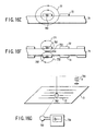
- FIG. 12 is a plan view showing the entire back side wiring member. Desired back side wirings 23 are formed by subjecting a copper-plated layer formed on a polymer film to a patterning and etching technique. A wiring resistance per back side wiring was 0.1 ohm. In addition, a part of the polymer film is removed and this film is divided into five regions 24a, 24b, 24c, 24d, 24e and 24f. As shown in FIG.
- these regions are arranged so as to correspond to a part connected with wiring electrode terminals 121 and 122 or the like of the rear panel, a side surface portion of the rear panel and the back surface portion of the rear panel and others, and they act as a support which prevents the back side wirings from being electrically shortcircuited in the assembly process or from being disconnected due to mechanical shock or the like.
- the drive IC 32 is arranged at a space portion of base films 24c and 24d and connected as shown in FIG. 11. It is to be noted that the surface of the copper wiring at the connection portion is preferably covered with a corrosion-resistant conductive film of e.g., gold, silver, nickel, solder, etc., to ensure good connection. In this embodiment, the copper surface of the connection portion is covered with the two-layer structure of copper/nickel/solder. ) Additionally, an anisotropic conductive film 31 is used for connection, and many connections are collectively performed.
- a corrosion-resistant conductive film e.g., gold, silver, nickel, solder, etc.
- FIG. 13 is a plan view showing the back side of the complete panel.
- the scanning line wirings are connected at the both ends through the back side wirings 23, these back side wirings 23 are connected to the drive ICs 32 (32a, 32b, ...), and the drive ICs 32 are connected to a circuit board 34 having a control circuit formed thereto.
- the electrode terminals of the signal line wirings at the both ends thereof are connected through the back side wirings 43, and driven by drive ICs 52 (52a, 52b, ). These drive ICs 52 are connected to a circuit board 53 and receive signals.
- the operation is substantially the same as that when arranging the drive ICs on the both sides of the panel. Therefore, the brightness inclination of the display panel is substantially symmetrical, and can greatly improve the display quality as compared with the case that the display panel is driven from one side. Further, only one drive IC is provided for one wiring even though driving from the both sides is realized, thereby avoiding an increase in cost and power consumption.
- FIG. 14 is a plan view showing a schematic structure of a matrix type display apparatus according to a second embodiment of the present invention.
- the back side wirings 23 on the back side of the rear plate 11 are provided on only the scanning line side, and the back side wiring connection portion of the drive ICs 32 (32a, 32b, ...) is provided at the central part of the back side wirings.
- These drive ICs 32 are connected to the circuit board 34 on which the control circuit is mounted.
- Reference numerals 24b to 24e denote polymer films which function as the base of the back side wirings 23.
- FIG. 15A show drive pulse waveforms of this panel.
- Voltage pulses of 61a, 61b, ... are sequentially applied to the scanning line wirings.
- a pulse width of the drive pulse is 30 ⁇ seconds
- a cycle Tf is 16.67 ms (60 Hz)
- a pulse voltage is -8V.
- voltage pulses of 62a, 62b, ... are applied to the signal line wirings, respectively.
- the voltage pulses of the signal line wirings and those of the scanning line wirings are applied in synchronization with each other.
- a maximum pulse width of the voltage pulses of the signal line wirings is 30 ⁇ m, and the pulse width is narrowed when the brightness is insufficient.
- a voltage value is 8 V.
- a voltage of 16 V is applied to the electron source of the pixel portion where a selection voltage of -8 V is applied to the scanning line wiring and a display voltage of 8 V is simultaneously applied to the signal line, and the electron is emitted from the electron source.
- the emitted electron is accelerated at the anode electrode to which a high voltage is applied (6 kV in this embodiment), injected into the luminescent material layer, and emits light.
- a resistance per scanning line wiring is approximately 0.6 ⁇ , and a voltage difference of 0.32 V is generated at the drive end and the electrode terminal portion provided on the side opposite to the drive end (in the case of a simple resistance ⁇ current model) when passing all the currents from one electrode terminal of the scanning line wiring.
- a voltage drop of 0.23 V corresponds to a difference of approximately 30% when converted to an emitted electron flow. That is, when driving from one side, there is provided the brightness inclination of 30% on the right and left sides of the screen under this condition. This state is indicated by 65 in FIG. 15B.
- the both-side driving requires the drive ICs whose number is twofold that of the drive ICs in the one-side driving in the prior art, the drive ICs whose number is equal to that in the one-side driving can realize the same excellent display quality as that of the both-side driving in this embodiment.
- the back side wirings are provided on only the scanning line side in this embodiment. That is because the current flowing into the signal line corresponds to one selected pixel in the matrix type display panel using this electron source, and the current is as small as 1 mA or below, which is not affected by the wiring resistance.
- the electron source current is large, when the leak current of the non-selected electron source is large, or when the wiring resistance is considerably high, providing the back side wirings on both the scanning line side and the signal line side can improve the display image quality like the first embodiment.
- FIG. 15B shows an in-screen brightness distribution in the first embodiment. Since the drive IC 32 is not provided at the central part of the back side wirings, the resistance of the back side wirings has an impact. However, since the resistance per back side wiring is as small as 0.1 ⁇ , the impact is slight, and a reduction in the maximum brightness is also not more than 10%.
- the back side wiring resistance is not negligible with respect to wirings on the rear panel, it is desirable to drive from the vicinity of the central part of the back side wirings like the second embodiment. Specifically, when the back side wiring resistance is larger than the resistance of the scanning lines or the signal lines connected with the back side wirings, driving from the central part is desirable.
- the display signal is applied to each of the pixels of the million order, and hence electrical signals used for display are transferred at a high speed. Therefore, the electromagnetic noise is radiated from the display panel including the peripheral drive circuits, and such noises must be restricted.
- the pulse current of 0.38 A flows through each scanning line, and the electromagnetic noise corresponding to this flow of current is thus radiated.
- the pulse voltage of 15V with a width of 30 ⁇ s and a cycle of 60 Hz is sequentially applied to the scanning line wirings of the rear plate (FIGS. 16A and 16B) having the conventional structure.
- FIG. 16A shows the one-side driving
- FIG. 16B shows the both-side driving in the conventional structure.
- FIG. 16C shows driving of the rear plate according to this embodiment, and the same pulse voltage was applied from the central part of the back side wirings 74.
- the radiant noise was measured on a front surface 751 of the rear plate, in a direction 752 vertical to the scanning line wirings in the plane of the rear plate and in a direction 753 parallel to the scanning line wirings in the plane of the rear plate.
- measurement was carried out at a position away from the central part of the rear panel by 2 m.
- FIG. 16E shows the cross section of the rear plate having the conventional structure, and a magnetic field 77 is generated around a current 761 when the current 761 (reference symbol indicates that the current direction runs from underneath to the surface of the page) flows through the wiring 72.
- a spatial distribution of this magnetic field is basically concentric, and becomes equal in the vertical direction of the substrate 71 and the horizontal direction in the drawing.
- the wiring system forms a loop
- the magnetic field is small in the vertical direction of the rear plate but the magnetic field has a double intensity in the horizontal direction of the substrate. That is, the back side wirings of this embodiment form one kind of loop antenna, and the radiant noise has directivity.
- the wiring groups arranged in parallel constitute an antenna system which increases the directivity. Therefore, it was found that the structure of this embodiment can greatly reduce the radiant noise in the vertical direction of the display panel.
- the radiant noise increases in the direction of 752 in FIG. 16D but provision of a shield plate 754 or the like which blocks off the electromagnetic noise to a casing can suppress the radiant noise.
- this anode electrode is formed on the face plate opposed to the substrate 71 in the display panel of this embodiment, this anode electrode is generally a very thin film of Al with a thickness of approximately 0.1 ⁇ m which reflects the emitted light from the luminescent material layer, thus shielding of the radiant noise is difficult.
- the matrix type luminescent display panel which is of the electron beam excited type using the field emission type electron sources
- a high voltage of several kV is applied to the anode electrode.
- Discharge due to foreign particles in the panel may occur between the rear plate and the face plate in some cases. In such a case, the discharge current instantaneously flows through the matrix wirings.
- This impulsive noise has a high voltage and hence is greater than the radiant noise generated in the regular operation by a single digit or more.
- FIG. 16G shows an experimental method of the radiant noise caused due to discharge, and a high voltage is applied to a capacitor 781 in advance and its charge is discharged (782) to the wirings on the rear plate.
- the noise generated at that moment was received by a small loop antenna and a generated voltage was measured by using an oscilloscope.
- the magnitude of the electromagnetic noise radiated in the direction of the front surface of the rear plate can be reduced to approximately 1/10 in the rear plate according to this embodiment, as compared with the rear plate wiring structure having the conventional structure. It was revealed that the electromagnetic radiant noise generated from the display panel can be greatly reduced by the back side wiring structure as described above.
- the effect is particularly high in the electron beam excited type luminescent material display panel using a high voltage, an electroluminescent type display panel having a high pulse voltage, an ultraviolet ray excited type luminescent material display panel having a high pulse voltage and a high drive frequency (so-called plasma display) and the like.
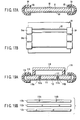
- FIGS. 17A and 17B are a cross-sectional view and a plan view showing a schematic structure of a matrix type display panel according to a third embodiment of the present invention.
- the mode, the number of pixels, etc., of the display panel are equal to those in the second embodiment, but the back side wirings are formed of thin-film wirings in this embodiment. That is, after forming scanning line wirings 92 as well as an interlayer insulating film and signal line wirings, which are not shown, on the front side of a glass substrate 91 as the rear plate, a chrome thin film with a thickness of 0.1 ⁇ m is formed on the back side by the sputtering method, and a copper thin film with a thickness of 20 ⁇ m and a nickel thin film with a thickness of 0.1 ⁇ m are formed by sputtering. Thereafter, back side wirings 93 are formed by patterning of a photoresist and succeeding etching. Then, planar electron sources are formed on the surface of the rear plate, and the rear plate is positioned, sealed and bonded with the face plate. Then, the inside of the display cell is vacuum-pumped through a non-illustrated exhaust tube.
- the scanning line wirings 92 on the surface of the rear plate are connected with the back side wirings 93 by using wirings 95 which are formed on a polymer film 94 at the end surface portions of the substrate and mainly include copper.
- the drive ICs are connected to the back side wirings 93, and they are further connected to a control circuit, thereby completing the display panel.
- using the thin-film wirings as the back side wirings 93 can directly form the back side wirings 93 on the back side of the substrate, which results in advantages such as a decrease in the number of components or reduction in thickness of the panel, amongst others.
- a copper or copper alloy foil may be etched and punched out as another method of forming the back side wirings.
- the back side wirings since the thickness of the wirings can be increased, the back side wirings with a low resistance can be realized.
- Such wirings may be bonded on the back side of the rear plate in order to form the back side wirings appressed against the substrate such as shown in FIGS. 17A and 17B.
- regular electric wires covered with an organic insulating film or a so-called enameled wire having an insulating substance applied on the surface thereof may be likewise used. In this case, it is recommendable to tightly align and fix several wires in parallel and flatly.
- a so-called flat cable it can be readily connected with an all-purpose connector which facilitates connection with the drive IC or the drive circuit board, thereby enabling assured connection in a simple process.
- FIGS. 18A and 18B are cross-sectional views showing a schematic structure of a matrix type display apparatus according to a fourth embodiment of the present invention, and FIG. 18C is a plan view.
- an electroluminescence material is used for a luminescent layer.
- the basic structure is the same as that shown in FIG. 10, and the number of scanning line wirings is 480 while the number of signal line wirings is 640. Pixels are defined at intersection areas of scanning line wirings 102 (102a, 102b, ...) and signal line wirings 103 (103a, 103b, 103c ). That is, applying the electric field to the insulating layer including the luminescent layer sandwiched between the overlap parts of the both wirings can provoke emission of light, and this whole area acts as display pixels.
- FIG. 18A is a cross-sectional view showing a display panel
- FIG. 18B is an enlarged cross-sectional view showing a pixel area (indicated by 18B in FIG. 18A)
- FIG. 18C is a plan view.
- Scanning line wirings 102 are formed of a chrome thin film on the front side of a substrate 101, an MgO dielectric material layer 104 and a luminescent layer 105 mainly including ZnS are superimposed and formed on the scanning line wirings 102, and signal line wirings 103 are formed on these layers. That is, the dielectric material layer 104 and the luminescent layer 105 are sandwiched and provided between the both wirings 102 and 103.
- the signal line wiring 103 is formed by a transparent electrode (ITO film is used in this embodiment), and transmits light from the luminescent layer 105 therethrough. Further, each signal line wiring 103 on the front side of the substrate is protected by a nitride film (SiNx) 106.
- ZnS which emits monochromatic light is used for the luminescent material layer, but full-color display is also enabled by forming luminescent materials for red luminescence, green luminescence and blue luminescence in accordance with each pixel (FIG. 18B).
- the back side wirings are formed by thin film wirings 93, and wirings 95 formed on polymer films 94 at end surface portions of the substrate and mainly including copper are used to connect the thin film wirings 93 on the back side of the substrate with the scanning line wirings 102.
- the drive IC is provided at the central part of the back side wirings although not shown.
- back side wirings are not restricted to the above-described type and, like FIG. 14 of the second embodiment, back side wirings 23 each of which is based on a polymer film and mainly including copper may be connected at both ends of the scanning line wiring 102 and provided on the back side.
- the dielectric material is formed between the both wirings, and this can be basically regarded as wirings of the capacitive load. Therefore, as the circuit configuration of the output portion of the drive IC, such a CMOS structure as shown in FIG. 9A is desirable, and supply of the current from the drive IC is stopped when the wirings are charged up and reach a predetermined potential.
- the chrome thin film is used for the scanning line
- the wiring resistance is approximately 10 k ⁇
- the wiring capacitance is 600 pF
- the simple wiring time constant is 6 ⁇ s (microseconds).
- the number of drive ICs is one, and such problems do not occur. That is, in the electroluminescence display panel according to this embodiment, driving from the both sides is enabled with the minimum number of the drive ICs equal to that of conventional one-side driving, no brightness inclination occurs, and display with the excellent uniformity can be realized. Also, the effect that generation of the excessive power consumption can be suppressed was confirmed.
- FIG. 19A is a cross-sectional view showing a schematic structure of a matrix type display panel according to a fifth embodiment
- FIG. 19B is a plan view showing the same.
- the mode of the display panel, the number of pixels and others are equal to those of the third embodiment.
- the back side wirings and the wirings on the rear plate to be connected with the back side wirings are connected to each other via conductive through holes provided on the substrate.
- the through hole is first formed by ultrasonic processing at a position on the glass substrate 111 as the rear plate where the scanning line wiring is formed.
- Conductive portions 116 (116a, 116b) are lined by the silver paste on the inner glass surfaces of the through holes 116, and the remaining hollow portions are filled with frit glass 117 (117a, 117b) and sintered.
- two conductive through holes are formed for each scanning line wiring. Additionally, as to positions of the holes, as shown in FIG. 19B, the holes are arranged in such a manner that their positions are shifted from each other at adjacent wiring portions thus damage to the substrate due to concentration of stress at a specific position of the substrate is not generated.
- a chrome thin film having a thickness of 0.1 ⁇ m is formed on the back side by the sputtering method, and a copper thin film having a thickness of 20 ⁇ m and a nickel thin film having a thickness of 0.1 ⁇ m are further formed by the sputtering method.
- the back side wirings 113 are formed by patterning a photoresist and successive etching.
- the back side wirings are formed at positions which match with the corresponding through holes of the scanning line wirings.
- planar electron sources are formed on the surface of the rear plate, the rear plate is positioned with the face plate, and they are sealed and bonded with each other. Further, the inside of the display cell is vacuum-pumped through a non-illustrated exhaust tube.
- the wirings 115 which are formed on the polymer films 114 at the end surface portions of the substrate and mainly include copper are used to connect the scanning line wirings 112 on the surface of the rear plate with the back side wirings 113.
- the drive IC is connected with the back side wirings 113, and they are further connected with the control circuit, thereby completing the display panel.
- the back side wirings 113 are provided on the back side of the rear plate 111 and connected with the both end portions of the scanning line wirings 112, the voltage drop due to the wiring resistance of the scanning line wirings 112 can be reduced. Furthermore, since the drive pulse voltage can be applied to the central part of the scanning line wirings 112 from the back side wirings 113 side via the through holes, a decrease in voltage can be further reduced. Therefore, the uniformity of display can be further improved. Specifically, irregularities in brightness of display can be improved to 2% or below.
- the through hole in this embodiment can be applied to the substrate of the electroluminescence display panel shown in FIG. 18A of the fourth embodiment.
- FIG. 20 is a plan view showing a schematic structure of a matrix type display panel according to a sixth embodiment of the present invention.
- This embodiment is an example of a plasma display which causes a luminescent material to emit light by ultraviolet ray excitation using plasma discharge.
- Drive pulses are applied to scanning line wirings 124 (124a, 124b, 124c, ...) from a non-illustrated scanning line driver circuit, and drive pulses are applied to signal line wirings 126 (126a, 126b, 126c, ...) from the non-illustrated signal line driver circuit.
- one discharge is effected by one application of the voltage pulse and discharge is not sustained, and hence a plurality of discharges must be generated in order to control the brightness.
- Continuing application of the pulse voltage after the first discharge can sustain discharge for the number of pulse applications by the memory effect, thereby enabling brightness control.
- Wirings to sustain this discharge are 125 (125a, 125b, 125c, ...), and the voltage is supplied from a non-illustrated sustaining pulse driver circuit.
- Pixels 127 are defined at intersections of the scanning lines, the signal lines and the sustaining voltage wirings. It is to be noted that reference numeral 128 in the drawing denotes a partition used to avoid discharge due to malfunction of the adjacent pixels.
- FIG. 21 shows a cross section of the plasma display panel, and scanning line wirings 124 and sustaining pulse wirings 125 (not shown) are formed on the front side of a glass substrate (first substrate) 131. Moreover, although not shown, a dielectric material film and others are formed on the wirings.
- An opposed substrate (second substrate) 135 is provided with its front surface being opposed to that of the glass substrate 131, signal line wirings 126 are formed on the front surface of the substrate 135, and a luminescent material layer 137 is provided thereon.
- the substrates 131 and 135 are supported with a predetermined gap maintained therebetween in such a manner that the respective wirings 124 and 126 are aligned so as to be orthogonal to each other, and a discharge gas is filled between the both substrates.
- Back side wirings 139 are provided on the back side of the second substrate 135, and these back side wirings 139 are provided so as to extend to the both sides of the second substrate 135 and connected with the scanning line wirings 124 on the first substrate 131 side at the both end portions of the substrate.
- connecting the back side wirings 139 provided on the second substrate 135 side with the scanning line wirings 124 provided on the first substrate 131 side at the both end portions can reduce the voltage drop due to the wiring resistance of the scanning line wirings 124 and restrict the unevenness of the brightness.
- the present invention is not restricted to each of the above embodiments.
- the electron beam excited type display apparatus using the planar electron sources or the electroluminescence type display apparatus has been described in the foregoing embodiments, the present invention is not restricted thereto, and it is possible to adopt any other excited electron beam type display apparatus, e.g., an apparatus which is of a type using Spindt electron sources or electron sources using carbon nanotubes.
- any other display apparatus e.g., a display apparatus based on LED type light emitting elements using an organic material, or a luminescent material display apparatus based on plasma discharge and ultraviolet ray excitation.
- any luminescent display panel in which pixels are arranged in the form of a matrix and the respective pixels are driven by scanning lines and signal lines formed in directions substantially orthogonal to each other can demonstrate the advantages of the invention.
- the back side wirings may be formed by screen printing using an Ag paste.
- the scanning line wirings or the signal line wirings of the substrate are formed by the Ag paste wirings, warpage of the glass substrate due to thermal expansion can be advantageously minimized.
- the back side wirings are provided to connect the both ends of at least either the scanning line wirings or the signal line wirings, it is possible to realize a matrix type display panel which has the same excellent image quality as that obtained from two-side driving, superior in evenness of display with the same minimum number of drive ICs as that in the conventional one-side driving, minimizes power consumption, and has a stable operation with reduced electromagnetic radiant noise.
Landscapes
- Engineering & Computer Science (AREA)
- Physics & Mathematics (AREA)
- General Physics & Mathematics (AREA)
- Theoretical Computer Science (AREA)
- Computer Hardware Design (AREA)
- Cathode-Ray Tubes And Fluorescent Screens For Display (AREA)
- Devices For Indicating Variable Information By Combining Individual Elements (AREA)
- Control Of Indicators Other Than Cathode Ray Tubes (AREA)
- Gas-Filled Discharge Tubes (AREA)
Applications Claiming Priority (3)
| Application Number | Priority Date | Filing Date | Title |
|---|---|---|---|
| JP2001242370A JP3607647B2 (ja) | 2001-08-09 | 2001-08-09 | マトリックス型表示パネル |
| JP2001242370 | 2001-08-09 | ||
| PCT/JP2002/003761 WO2003017238A1 (fr) | 2001-08-09 | 2002-04-16 | Appareil d'affichage du type matriciel |
Publications (1)
| Publication Number | Publication Date |
|---|---|
| EP1416460A1 true EP1416460A1 (fr) | 2004-05-06 |
Family
ID=19072650
Family Applications (1)
| Application Number | Title | Priority Date | Filing Date |
|---|---|---|---|
| EP20020717167 Withdrawn EP1416460A1 (fr) | 2001-08-09 | 2002-04-16 | Appareil d'affichage du type matriciel |
Country Status (6)
| Country | Link |
|---|---|
| EP (1) | EP1416460A1 (fr) |
| JP (1) | JP3607647B2 (fr) |
| KR (1) | KR100537118B1 (fr) |
| CN (1) | CN1465037A (fr) |
| TW (1) | TW556243B (fr) |
| WO (1) | WO2003017238A1 (fr) |
Cited By (2)
| Publication number | Priority date | Publication date | Assignee | Title |
|---|---|---|---|---|
| EP1533852A3 (fr) * | 2003-11-21 | 2010-05-05 | Semiconductor Energy Laboratory Co., Ltd. | Dispositif d'affichage électroluminescent organique |
| US11626468B2 (en) | 2018-07-03 | 2023-04-11 | Lg Display Co., Ltd. | Multi-panel organic light emitting display device |
Families Citing this family (11)
| Publication number | Priority date | Publication date | Assignee | Title |
|---|---|---|---|---|
| US10261370B2 (en) | 2011-10-05 | 2019-04-16 | Apple Inc. | Displays with minimized border regions having an apertured TFT layer for signal conductors |
| US9286826B2 (en) | 2011-10-28 | 2016-03-15 | Apple Inc. | Display with vias for concealed printed circuit and component attachment |
| US9226347B2 (en) | 2012-06-25 | 2015-12-29 | Apple Inc. | Displays with vias |
| US9214507B2 (en) | 2012-08-17 | 2015-12-15 | Apple Inc. | Narrow border organic light-emitting diode display |
| US9454025B2 (en) | 2012-08-31 | 2016-09-27 | Apple Inc. | Displays with reduced driver circuit ledges |
| CN202816322U (zh) * | 2012-09-19 | 2013-03-20 | 深圳市柔宇科技有限公司 | 一种显示屏 |
| KR102655727B1 (ko) * | 2017-10-19 | 2024-04-08 | 엘지디스플레이 주식회사 | 표시 장치 및 표시 장치 제조 방법 |
| KR102527303B1 (ko) * | 2017-10-31 | 2023-04-27 | 엘지디스플레이 주식회사 | 발광 표시 장치 |
| KR102515399B1 (ko) * | 2017-12-12 | 2023-03-28 | 엘지디스플레이 주식회사 | 배선 필름 및 그를 포함한 표시 장치 |
| WO2021107145A1 (fr) * | 2019-11-29 | 2021-06-03 | 京セラ株式会社 | Dispositif d'affichage |
| CN113644085B (zh) * | 2020-08-14 | 2023-06-02 | 友达光电股份有限公司 | 电子装置及电子装置的制造方法 |
Family Cites Families (8)
| Publication number | Priority date | Publication date | Assignee | Title |
|---|---|---|---|---|
| JPH03116597U (fr) * | 1990-03-09 | 1991-12-03 | ||
| JPH04229529A (ja) * | 1990-12-26 | 1992-08-19 | Mitsubishi Electric Corp | 気体放電表示装置 |
| JPH05150252A (ja) * | 1991-11-29 | 1993-06-18 | Kyocera Corp | 液晶表示装置 |
| JPH05323354A (ja) * | 1992-05-19 | 1993-12-07 | Fujitsu Ltd | 液晶表示装置 |
| JP4366743B2 (ja) * | 1998-09-11 | 2009-11-18 | ソニー株式会社 | 平面表示装置 |
| JP3619085B2 (ja) * | 1999-02-18 | 2005-02-09 | キヤノン株式会社 | 画像形成装置、その製造方法及び記憶媒体 |
| JP4212184B2 (ja) * | 1999-05-10 | 2009-01-21 | 株式会社日立製作所 | プラズマディスプレイ装置 |
| JP3915379B2 (ja) * | 2000-07-31 | 2007-05-16 | セイコーエプソン株式会社 | 液晶装置および電子機器 |
-
2001
- 2001-08-09 JP JP2001242370A patent/JP3607647B2/ja not_active Expired - Fee Related
-
2002
- 2002-04-16 WO PCT/JP2002/003761 patent/WO2003017238A1/fr not_active Application Discontinuation
- 2002-04-16 CN CN02802614A patent/CN1465037A/zh active Pending
- 2002-04-16 KR KR10-2003-7004953A patent/KR100537118B1/ko not_active IP Right Cessation
- 2002-04-16 EP EP20020717167 patent/EP1416460A1/fr not_active Withdrawn
- 2002-04-16 TW TW091107774A patent/TW556243B/zh not_active IP Right Cessation
Non-Patent Citations (1)
| Title |
|---|
| See references of WO03017238A1 * |
Cited By (2)
| Publication number | Priority date | Publication date | Assignee | Title |
|---|---|---|---|---|
| EP1533852A3 (fr) * | 2003-11-21 | 2010-05-05 | Semiconductor Energy Laboratory Co., Ltd. | Dispositif d'affichage électroluminescent organique |
| US11626468B2 (en) | 2018-07-03 | 2023-04-11 | Lg Display Co., Ltd. | Multi-panel organic light emitting display device |
Also Published As
| Publication number | Publication date |
|---|---|
| KR100537118B1 (ko) | 2005-12-16 |
| CN1465037A (zh) | 2003-12-31 |
| KR20030041153A (ko) | 2003-05-23 |
| TW556243B (en) | 2003-10-01 |
| JP3607647B2 (ja) | 2005-01-05 |
| WO2003017238A1 (fr) | 2003-02-27 |
| JP2003058074A (ja) | 2003-02-28 |
Similar Documents
| Publication | Publication Date | Title |
|---|---|---|
| KR100470282B1 (ko) | 다층세라믹기판을가지는모자이크식일렉트로루미네선스디스플레이 | |
| EP1416460A1 (fr) | Appareil d'affichage du type matriciel | |
| US7375465B2 (en) | Plasma display panel with single sided driving circuit | |
| JPH03295138A (ja) | 表示装置 | |
| CN1471699A (zh) | 发光板中的微量组分的激励系统和激励方法 | |
| KR20040055567A (ko) | 냉음극형 플랫 패널 디스플레이 | |
| JPH0728414A (ja) | 電子ルミネッセンス表示システム | |
| CN101325140B (zh) | 电子源和图像显示设备 | |
| US20040201551A1 (en) | Matrix type display apparatus | |
| US6960111B2 (en) | Manufacturing methods for electron source and image forming apparatus | |
| US20070080646A1 (en) | Flat display unit | |
| US8207911B2 (en) | Display device | |
| KR20040090796A (ko) | 평판 디스플레이 패널 구동방법 | |
| CN101398990A (zh) | 等离子显示装置 | |
| EP2235732B1 (fr) | Dispositif à émission de champ à gradation locale fine | |
| CN101308749A (zh) | 等离子体显示器用实验测试屏 | |
| TWI281686B (en) | Image display device | |
| CN101174538A (zh) | 发光装置与显示装置 | |
| JP2789210B2 (ja) | 電子線発生装置及び該電子線発生装置を用いた画像形成装置 | |
| KR100824465B1 (ko) | 면방전 교류 플라즈마 디스플레이 패널의 전극구조 | |
| KR20020029565A (ko) | 전계 방출 표시소자 | |
| TWI240238B (en) | Method for driving plasma display panel | |
| JP2000260303A (ja) | 電子源及び画像形成装置 | |
| Li et al. | Development of a 25‐in. SVGA SMPDP | |
| KR20070059515A (ko) | 아크 측정이 가능한 전자방출표시소자 및 아크 측정방법 |
Legal Events
| Date | Code | Title | Description |
|---|---|---|---|
| PUAI | Public reference made under article 153(3) epc to a published international application that has entered the european phase |
Free format text: ORIGINAL CODE: 0009012 |
|
| 17P | Request for examination filed |
Effective date: 20030407 |
|
| AK | Designated contracting states |
Kind code of ref document: A1 Designated state(s): DE FR GB IT NL |
|
| STAA | Information on the status of an ep patent application or granted ep patent |
Free format text: STATUS: THE APPLICATION HAS BEEN WITHDRAWN |
|
| 18W | Application withdrawn |
Effective date: 20080125 |