EP1410158B1 - Circuit electronique avec commande de l'energie - Google Patents
Circuit electronique avec commande de l'energie Download PDFInfo
- Publication number
- EP1410158B1 EP1410158B1 EP02747347A EP02747347A EP1410158B1 EP 1410158 B1 EP1410158 B1 EP 1410158B1 EP 02747347 A EP02747347 A EP 02747347A EP 02747347 A EP02747347 A EP 02747347A EP 1410158 B1 EP1410158 B1 EP 1410158B1
- Authority
- EP
- European Patent Office
- Prior art keywords
- controller
- energy
- electronic circuit
- clock
- peripheral devices
- Prior art date
- Legal status (The legal status is an assumption and is not a legal conclusion. Google has not performed a legal analysis and makes no representation as to the accuracy of the status listed.)
- Expired - Lifetime
Links
Images


Classifications
-
- G—PHYSICS
- G06—COMPUTING OR CALCULATING; COUNTING
- G06F—ELECTRIC DIGITAL DATA PROCESSING
- G06F1/00—Details not covered by groups G06F3/00 - G06F13/00 and G06F21/00
- G06F1/26—Power supply means, e.g. regulation thereof
-
- G—PHYSICS
- G06—COMPUTING OR CALCULATING; COUNTING
- G06K—GRAPHICAL DATA READING; PRESENTATION OF DATA; RECORD CARRIERS; HANDLING RECORD CARRIERS
- G06K19/00—Record carriers for use with machines and with at least a part designed to carry digital markings
- G06K19/06—Record carriers for use with machines and with at least a part designed to carry digital markings characterised by the kind of the digital marking, e.g. shape, nature, code
- G06K19/067—Record carriers with conductive marks, printed circuits or semiconductor circuit elements, e.g. credit or identity cards also with resonating or responding marks without active components
- G06K19/07—Record carriers with conductive marks, printed circuits or semiconductor circuit elements, e.g. credit or identity cards also with resonating or responding marks without active components with integrated circuit chips
- G06K19/0701—Record carriers with conductive marks, printed circuits or semiconductor circuit elements, e.g. credit or identity cards also with resonating or responding marks without active components with integrated circuit chips at least one of the integrated circuit chips comprising an arrangement for power management
-
- G—PHYSICS
- G06—COMPUTING OR CALCULATING; COUNTING
- G06K—GRAPHICAL DATA READING; PRESENTATION OF DATA; RECORD CARRIERS; HANDLING RECORD CARRIERS
- G06K19/00—Record carriers for use with machines and with at least a part designed to carry digital markings
- G06K19/06—Record carriers for use with machines and with at least a part designed to carry digital markings characterised by the kind of the digital marking, e.g. shape, nature, code
- G06K19/067—Record carriers with conductive marks, printed circuits or semiconductor circuit elements, e.g. credit or identity cards also with resonating or responding marks without active components
- G06K19/07—Record carriers with conductive marks, printed circuits or semiconductor circuit elements, e.g. credit or identity cards also with resonating or responding marks without active components with integrated circuit chips
- G06K19/0723—Record carriers with conductive marks, printed circuits or semiconductor circuit elements, e.g. credit or identity cards also with resonating or responding marks without active components with integrated circuit chips the record carrier comprising an arrangement for non-contact communication, e.g. wireless communication circuits on transponder cards, non-contact smart cards or RFIDs
Definitions
- the present invention relates to electronic Circuits with a controller and in particular to the Control of the controller in these electronic circuits.
- CMOS complementary metal-oxide-semiconductor
- CMOS complementary metal-oxide-semiconductor
- DESoder AES symmetric encryption method
- cryptography controllers become, for example in smart cards, e.g. SIM cards or signature cards, for example, for payment with the mobile phone, for Home banking transactions or legally binding electronic Signatures used.
- cryptography controllers in computers or servers as a security IC used to perform an authentication, or to Encryption tasks to be able to take which, for example from the secure transmission of credit card numbers, the transmission of Emails secret contents and the secure cashless payments via the Internet can.
- cryptographic controllers must have a high computing power have to be the ones for the respective cryptographic Algorithm required calculations in appropriate Time to perform. For example, it would be for one User unreasonable, several minutes on an authentication check or a payment transaction wait have to. To achieve this high computing power, Known cryptographic controllers handle many of the things to do Arithmetic operations in parallel to the computational speed to increase.
- a potential design for a cryptography controller that On the one hand a high multi-functionality and on the other hand a high processing speed, consists of a composite of a central processing unit and one or more coprocessors working in parallel, as is the case with modern PCs, but also with modern ones Graphics cards is the case, and which via a bus system connected to each other.
- the coprocessors take over In this case complex arithmetic tasks, for example, certain Cryptographic algorithms or specific arithmetic operations are assigned, such.
- Terminals for Contact-based smart cards provide, for example, a maximum Current of a few mA, taking contactless applications and mobile applications, such.
- B. a SIM card in a cell phone the power may even be limited to less than 10 mA can. Consequently, the computational speed of coprocessors limited by the available energy.
- the clock frequency with which the CPU and the crypto-coprocessors are subject to restrictions by the Energy available as with the implementation of the controller chip in CMOS technology the power consumption of the Clock frequency or the switching frequency of the MOSFETs depends.
- the object of the present invention is to provide a electronic circuit and a method for controlling a to create electronic circuit, so that at the same to Available energy the computing power is increased.
- An electronic circuit comprises a Controller for processing a processor task and a Energy determination device for determining the for the controller available energy.
- a control device the electronic circuit controls the controller from the energy available to the controller.
- An inventive method for controlling an electronic Circuit which is a controller for processing a Processor task includes determining the for the Controller available energy as well as controlling of the controller depending on which is available for the controller standing energy.
- the present invention is based on the finding that by determining which for the controller, e.g. a cryptography controller, available energy an optimization the computing time of an operation can be achieved by optimally determining the energy, for example relevant, i. for a present processor task mainly required coprocessors or other peripheral devices or the CPU of the controller is distributed. Even though for this purpose, the electronic circuit energy determination device or an energy meter is added, causing The complexity of the same can be increased by the the best possible use of energy on the one hand an improvement the computing power with constant circuit complexity and on the other hand, a reduced circuit complexity be achieved with constant computing power.
- the controller e.g. a cryptography controller
- the controller of the controller depending on the available for the controller standing energy performed by the controller clock, with which the controller is operated is raised, if more Energy is available, and is reduced if less Energy is available.
- the Controller clock according to the determined available energy tracked to make the best possible use of the available to achieve standing energy.
- the controller can do this be carried out that on the one hand to carry out the Processor task required computing time is minimized and In addition, the available energy is sufficient.
- the controller is controlled so that on the one hand to the Available energy to process the processor task is sufficient by the controller, and on the other hand, the respective Peripheral device or the respective coprocessor maximum amount of energy to perform the arithmetic task is assigned.
- the Available energy between a peripheral device and a CPU of the controller divided by, for example because of the few of the CPU during one RSA encryption work to be done, the CPU low clocked and the peripheral device, i. the responsible person Coprocessor for modular multiplications, high clocked becomes.
- the available energy primarily between two peripheral devices split by, for example, during an elliptic-curve encryption of this mainly provided coprocessor clocked high and a for Secondary calculations required coprocessor low clocked becomes. Overall, this results in a reduction of the required Calculation time with optimal energy utilization.
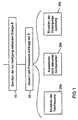
- FIG. 1 the invention Energy management and the benefits that result from it, described.
- Figs. 2 and 3 is then a Embodiment of an electronic circuit according to the present invention described.
- FIG. 4 is finally the application of the energy control of the invention in the case of contactless applications.
- the available energy E can vary for different reasons.
- the electronic circuit for chip cards for contact terminals can the energy available, for example, from Terminal to terminal or due to contact fluctuations between the contact terminal and the electronic Circuit vary. In contactless applications, the depends on Available energy E from the distance of a contact terminal terminal interface the chip card from the contact terminal from, as will be explained with reference to FIG. 4 in more detail becomes.
- the energy available due to the increasing discharge of the battery For mobile applications, such as B. in mobile phones, laptops or the like, the energy available due to the increasing discharge of the battery.
- the determination itself can be made in different ways or be carried out by means of different devices, taking various parameters as a measure of the available standing energy can be used, such. Legs Input voltage or a coupled current.
- a control of Controllers of the electronic circuit depending on the Available energy E which is determined in step 10 has been.
- the controller of the controller depends be carried out by the energy E in different ways in Fig. 1, only by way of example three possibilities 20a, 20b and 20c are shown.
- a first possibility 20a to control the controller consists in setting the Clock frequency of the controller depending on the available standing energy E. By changing the clock frequency is the Switching frequency of the switching elements forming the controller changed, for example, when implementing the controller in CMOS technology, a change in power consumption or the power consumption results.
- the clock frequency must be lower be adjusted while if more energy available stands, the clock frequency and thus the computing speed can be increased.
- the controller consists of several components can, as it referring will be explained in more detail in Fig. 2, the clock frequency for each component, e.g. a CPU or a peripheral device, such as. a coprocessor, individually adjusted become.
- the clock frequencies of the various Components can use the available energy E be fully exploited, or completely on all components required for the current processor task be distributed.
- the distribution of available Energy to the various components by adjusting The different clock frequencies may be in the sense of optimization the computing time of the processor task performed which is due to the computing time both by the maximum Exploiting the available energy as well through the simultaneous optimal distribution of energy the individual components is minimized.
- a second possibility 20b for controlling the controller exists in turning off controller components used for the current processor task is not relevant. These non-relevant controller components, for example by additional switching elements, e.g. FETs with low Leakage current, disconnected from the supply voltage to the same into a sleep mode.
- additional switching elements e.g. FETs with low Leakage current
- Another possibility 20c for controlling the controller consists in adjusting the supply voltage of the entire Controllers or individual components of the controller.
- the supply voltage could, for example, in the case that the available energy has a specific Threshold below, set to a lower value where the reliability of the controller operation less but still sufficient.
- the supply voltage for analog components of the electronic Circuit could be changed, such. B. for the analog Part of a contact terminal interface of the electronic Circuit.
- a main advantage of the above with reference to FIG. 1 described energy control is that in comparison to conventional electronic circuits used for a certain minimum supply energy are designed determines the available energy E and then is completely used up to operate the controller. In this way, also the minimum supply energy Exceeding share of available energy used for faster processing of the processor task become. While consequently in conventional electronic Circuits special peripheral devices that enhance the overall performance of the system, only operated in fixed predetermined multiples of a CPU clock be, and this is only possible if the Available energy can be sufficient through the Energy control according to the invention at excess available standing power individual peripheral devices higher be clocked so that the available Energy as possible, i. essentially completely, exploited is.
- the determined available energy optimal in terms of optimizing the computing time distributed to the relevant coprocessors so that the available energy is not just completely used up but also optimally exploited or used, whereby the computing speed of the controller at gleichereastender Energy increased and thus the user latency can be reduced at the terminal.
- an electronic will be hereinafter referred to Circuit according to an embodiment of the present invention Invention described.
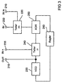
- Circuit according to this embodiment comprises the electronic circuit a cryptography processor and is arranged on a chip card for the application suitable for contactless terminals.
- the electronic circuit comprises a contact terminal terminal interface 100 and a cryptography processor, which consists of a CPU 110 and a peripheral device 120, such as a crypto-coprocessor, an RNA generator or a UART module, wherein in For ease of illustration, a crypto-coprocessor is assumed below as the peripheral device.
- the CPU 110 and the crypto-coprocessor 120 are each assigned a clock multiplier 130 and 140, respectively, which output a clock signal clock CPU or clock crypto to the CPU 110 and the crypto-coprocessor 120, and clock generators can be used instead of clock multipliers.
- the contact terminal interface 100 which is arranged to convert electromagnetic energy 105 from a contact terminal (not shown) into electrical energy for powering the electronic circuit, and consists of, for example, an antenna, a rectifier, and a low pass filter, supplies the supply power to both clock multipliers 130 and 140 as well as an energy meter 150.
- the energy meter 150 outputs control signals VC CPU and VC Krypto to the two clock multipliers 130 and 140, depending on the power available from the contact terminal interface 100, to control the clock frequencies of the clock signals of the clock multipliers 130 and 140 that are connected to the clocks CPU 110 and coprocessor 120 are output.
- the cryptography processor consisting of the CPU 110 and the crypto-coprocessor 120 is, for example, for processing certain processor tasks, such as one Encryption, decryption, authentication or signature based on the DES standard, the AES method, the RSA algorithm or the elliptic curve method.
- processor tasks such as one Encryption, decryption, authentication or signature based on the DES standard, the AES method, the RSA algorithm or the elliptic curve method.
- the Cryptocoprocessor 120 is in turn to perform a particular Arithmetic task provided, such as a modular or arithmetic addition, multiplication, exponentiation or inversions, a hash value calculation.
- a peripheral device 120 the same be an RNA generator, UART or sensor.
- the electrical energy that the contactlost terminal interface 100 extracts from the electromagnetic energy 105 is determined by the energy meter 150 and distributed to the CPU 110 and the crypto-coprocessor 120 by the clock multipliers 130 and 140 such that the CPU is supplied with the least possible energy, while the crypto-coprocessor 120, the maximum possible energy is provided.
- the distribution of the available energy to the CPU 110 and the crypto-coprocessor 120 the fact is exploited in the present case that changing the clock frequencies of the clock signals clock CPU and clock crypto of these components also determines the energy consumption of these components.
- the energy consumption depends on the switching frequency of the individual MOSFETs. Consequently, full utilization of the available energy is achieved by the fastest possible clocking of the crypto-coprocessor 120, which enables a high computing speed.
- the clock multipliers 130 and 140 are designed such that they output clock signals clock CPU and clock crypto with the same control signal whose clock frequencies differ by a fixed multiple n.
- the energy meter 150 it is also possible for the energy meter 150 to output differently high clock signals VC CPU and VC Krypto to the clock multipliers 130 and 140.
- the energy meter 150 is formed either as a regulator which converts the received supply energy from the contact terminal interface 100 into a voltage signal, as determined by a circuit design, such as, e.g.
- a linear regulator or includes an A / D converter to convert the supply energy into digital control signals VC CPU and VC Krypto .
- digital control signals a look-up table can be provided in which for certain supply energy ranges control signals VC CPU and VC Krypto are stored which ensure an optimum computing time of the cryptography processor for the respective supply energy range.
- the clock multipliers 130 and 140 of Fig. 2 are formed in the form of PLLs which allow clock frequency multiplication of an input frequency by rational multiples n / m.
- the input frequency is predetermined, for example, by a clock signal generated by the contact terminal interface 100.
- a block diagram of the clock multipliers 130 and 140 is shown in FIG.
- each clock multiplier comprises an input IN 200 to which the clock signal of the input frequency f in is applied, inputs INn and INm at which the value of the counter n and the denominator m of the rational multiple between the input frequencies f in and Output frequency f out is applied, and an output OUT, at which a clock signal with the clock frequency f out is output.
- the circuit comprises, in addition to a frequency divider 220, a PLL consisting of a voltage-controlled oscillator VCO 230, a frequency divider 240, an XOR circuit 250 and a regulator 260.
- One input of the frequency divider 220 is connected to the input IN 200 and another input to the input INm 210.
- the frequency divider 220 outputs an output signal of the frequency f in / m, the output being connected to an input of the XOR circuit 250.
- Another input of the XOR circuit 250 is connected to an output of the frequency divider 240, whose two inputs are connected to the input INn 205 and an output of the VCO 230, respectively.
- An input of the VCO 230 is connected through the regulator 260 to an output of the XOR circuit 250.
- the output of the VCO 230 is also connected to the output OUT 215.
- the control inputs INn and Inm which are controlled by the control signals VC CPU and VC crypto (see FIG. 2), can be used to set the divider ratios n and m (n, m ⁇ 1,2,3 ...), with which the frequency divider 220 and 240, the frequencies of the input clock signal at the input 200 and the output signal of the oscillator 230 share.
- the voltage controlled oscillator 230 is readjusted by the XOR circuit 250 in cooperation with the controller 260 in order to achieve the desired divider ratio between the input clock signal and the output clock signal. Consequently, the clock signal applied to the output OUT has the desired frequency f out .
- Fig. 4 shows schematically a chip card on which the electronic circuit of Fig. 2 is arranged, in three positions 300a, 300b and 300c relative to a contact terminal terminal 310 emitting an electromagnetic radiation 320 of a certain frequency.
- the various positions 300a-300c are at different exemplary distances, ie, 10 cm, 7 cm, and 5 cm, to the contactless terminal 310 Contactless terminal interface (see Fig.
- the electronic circuit depends on the distance d of the smart card from the contact terminal 310, at the various positions 300a, 300b and 300c depending on the distance of the smart card be set by the contactless terminal 310 higher or lower clock frequency f 1 , f 2 and f 3 for the controller of the electronic circuit. If the card is further away from the terminal 310, less power is available to the electronic circuitry, so the clock frequency must be lower. If the card comes closer to the terminal 310, more energy is available, so that the controller can be clocked at a higher clock frequency. In this way, the clock frequency is always adapted to the available energy, so that, when more energy is available, a lower computing time is made possible.
- a fixed power consumption such as a fixed clock frequency, for example, which corresponds to a certain maximum distance of the chip card from the terminal 310 and was a compromise of the widest possible range of distances and the highest possible computing power was. Consequently, operation of the cryptographic processor was only possible within this range, with the excess energy being dissipated at shorter intervals.
- a cryptography processor of a CPU and a peripheral device or a crypto-coprocessor In The more common cases become a cryptography processor however, more peripheral devices and crypto-coprocessors consist.
- the available standing energy such as, for example, the coprocessors be distributed, that a minimum computing time at maximum Energy utilization is achieved. This is achieved by at the distribution of available energy through the energy meter is determined on the coprocessors and the CPU additionally the current processor task and the different computing tasks of coprocessors and the associated tasks remaining peripheral devices taken into account become. The available energy will then always used for that or those coprocessors, in the application or the processor task on most claimed.
- Authentication becomes, for example, the crypto-coprocessor the maximum possible energy allocated during the CPU and the remaining coprocessors only a minimal proportion the available energy is allocated. On Similarly, the available energy goes through the fastest possible timing, for example in an encryption task on the DES module and in the calculation of the hash value to the hash module. For the current one Processor task non-relevant coprocessors can even completely switched off or put into a sleep mode be separated by the same from the supply voltage to avoid leakage currents.
- the optimal distribution of available energy among multiple coprocessors can be achieved by assigning a clock multiplier to each coprocessor, just as in FIG. 2 the clock multiplier 140 is assigned to the crypto-coprocessor 120.
- the CPU may be operated at the clock frequency f CPU
- the coprocessors that are not currently required in the processor task may be disabled or can be operated at the frequency f CPU
- only the crypto-coprocessor that is required in the application is clocked at a higher clock frequency, which is set so that the available energy is used up as completely as possible.
- optimization of computational speed and maximum power utilization is achieved by increasing or decreasing the clock frequency of the coprocessor currently being used primarily by the processor task, clocking it at the maximum possible clock frequency, and allowing the remaining available energy to operate the remaining required components is sufficient.
- each one optimized set of clock frequencies for the crypto-coprocessors is stored.
- Each set of clock frequencies would be the allocated energy available substantially distribute to those crypto-coprocessors whose associated Computing tasks in the associated application needed become.
- the clock frequencies within each set determined so that the available energy, of which this sentence is assigned, essentially completely used up becomes.
- the electronic circuit on both a circuit board can be arranged as well as integrated in a chip.
- the controller can either consist of individual components, which are arranged on a circuit board, or in be integrated into a single chip.
- the present invention relates to a contactless application has been described, is the present invention also on applications at contact terminals or on mobile Applications applicable.
- the contact terminal interface could of Fig. 2 by a simple contact be replaced.
Landscapes
- Engineering & Computer Science (AREA)
- Computer Hardware Design (AREA)
- Microelectronics & Electronic Packaging (AREA)
- Theoretical Computer Science (AREA)
- Physics & Mathematics (AREA)
- General Physics & Mathematics (AREA)
- Computer Networks & Wireless Communication (AREA)
- General Engineering & Computer Science (AREA)
- Power Sources (AREA)
- Executing Machine-Instructions (AREA)
- Control Of Electrical Variables (AREA)
- Feedback Control In General (AREA)
- Electronic Switches (AREA)
- Electrophonic Musical Instruments (AREA)
- Oscillators With Electromechanical Resonators (AREA)
- Ignition Installations For Internal Combustion Engines (AREA)
- Electrical Discharge Machining, Electrochemical Machining, And Combined Machining (AREA)
- Microcomputers (AREA)
Claims (13)
- Circuit électronique, qui comporte :et dans lequel le contrôleur (110, 120) a les caractéristiques suivantes :un contrôleur (110, 120) pour le traitement d'une tâche de processeur ;un dispositif de détermination d'énergie (150) pour la détermination de l'énergie mise à la disposition du contrôleur (110, 120); etun dispositif de commande (130, 140, 150) pour la commande du contrôleur (110, 120) en fonction de l'énergie mise à la disposition du contrôleur (110, 120),une multiplicité de dispositifs périphériques (120) pour l'exécution de tâches associées ; etune unité centrale de traitement (110) pour la commande de la multiplicité de dispositifs périphériques (120), etle dispositif de commande (130, 140, 150) est prévu pour commander la multiplicité de dispositifs périphériques (120) en fonction de la tâche de processeur, des tâches associées et de l'énergie mise à la disposition du contrôleur (110, 120).
- Circuit électronique selon la revendication 1, dans lequel le dispositif de commande (130, 140, 150) est prévu pour commander le contrôleur (110, 120) de telle sorte qu'une énergie nécessaire au contrôleur (110, 120) pour la tâche de processeur est sensiblement égale à l'énergie mise à la disposition du contrôleur (110, 120).
- Circuit électronique selon la revendication 1 ou 2, ayant aussi la caractéristique suivante :un dispositif de fourniture d'énergie (100) pour la production de l'énergie mise à la disposition du contrôleur (110, 120) à partir d'une énergie électromagnétique (105) amenée de l'extérieur.
- Circuit électronique selon l'une des revendications 1 à 3, qui est conçu comme un circuit intégré qui convient à une utilisation dans le cas de terminaux sans contact (310).
- Circuit électronique selon l'une des revendications 1 à 4, dans lequel le dispositif de commande (130, 140, 150) a la caractéristique suivante :un dispositif (130, 140) pour le réglage de l'horloge de contrôleur avec laquelle le contrôleur (110, 120) est exploité, la fréquence de l'horloge de contrôleur étant augmentée si plus d'énergie est disponible et étant réduite si moins d'énergie est disponible.
- Circuit électronique selon l'une des revendications 1 à 5, dans lequel le contrôleur (110, 120) est mis en oeuvre en technologie CMOS.
- Circuit électronique selon l'une des revendications précédentes, dans lequel le dispositif de commande (130, 140, 150) est prévu pour commander les dispositifs périphériques (120) de telle sorte que le temps de calcul nécessaire à l'exécution de la tâche de processeur par le contrôleur (110, 120) est minimisé.
- Circuit électronique selon l'une des revendications précédentes, dans lequel le contrôleur (110, 120) est un processeur de cryptographie et les dispositifs périphériques (120) sont des coprocesseurs cryptographiques (120) pour l'exécution de tâches de calcul, la tâche de processeur étant sélectionnée dans un groupe qui comprend cryptage, décryptage, authentification et signature selon le standard DES, selon le procédé AES, selon l'algorithme RSA et selon le procédé des courbes elliptiques et les tâches de calcul des coprocesseurs cryptographiques (120) étant sélectionnées dans un groupe qui comprend addition modulaire et addition non modulaire, multiplication, exponentiation, inverse, calcul de code hash et détermination de nombre aléatoire.
- Circuit électronique selon l'une des revendications précédentes, dans lequel le dispositif de commande (130, 140, 150) a aussi les caractéristiques suivantes :un dispositif pour le réglage des horloges de dispositifs périphériques avec lesquelles les dispositifs périphériques (120) sont exploités ; etun dispositif pour l'arrêt de certains des dispositifs périphériques (120).
- Circuit électronique selon la revendication 9, dans lequel le dispositif (140) pour le réglage des horloges de dispositifs périphériques (120) comporte un oscillateur qui est associé à l'un des dispositifs périphériques et qui produit un signal d'horloge ayant une fréquence d'horloge de sortie à laquelle le dispositif périphérique (120) associé est soumis.
- Circuit électronique selon la revendication 9, dans lequel le dispositif (140) pour le réglage des horloges de dispositifs périphériques (120) comporte un multiplicateur d'horloge qui est associé à l'un des dispositifs périphériques et qui produit un signal d'horloge ayant une fréquence d'horloge de sortie à laquelle le dispositif périphérique (120) associé est soumis.
- Circuit électronique selon l'une des revendications précédentes, dans lequel le contrôleur (110, 120) comporte un dispositif périphérique (120) pour l'exécution d'une tâche associée et une unité centrale de traitement (110) pour la commande du dispositif périphérique (120) et dans lequel le dispositif de commande (130, 140, 150) comporte un premier dispositif (130) pour le réglage d'une première horloge avec laquelle l'unité centrale de traitement (110) est exploitée et un deuxième dispositif (140) pour le réglage d'une deuxième horloge avec laquelle le dispositif périphérique (120) est exploité, la première et la deuxième horloge étant réglées de telle sorte que l'énergie mise à disposition suffit au traitement de la tâche de processeur et que simultanément l'énergie maximale possible est attribuée au dispositif périphérique (120) pour l'exécution de la tâche associée.
- Procédé pour la commande d'un circuit électronique qui comporte un contrôleur (110, 120) pour le traitement d'une tâche de processeur, le contrôleur (110, 120) comportant une multiplicité de dispositifs périphériques (120) pour l'exécution de tâches associées et une unité centrale de traitement (110) pour la commande de la multiplicité de dispositifs périphériques (120), le procédé ayant les étapes suivantes :détermination (10) de l'énergie mise à la disposition du contrôleur (110, 120) ; etcommande (20) du contrôleur (110, 120) en fonction de l'énergie mise à la disposition du contrôleur (110, 120), la commande étant effectuée pour commander la multiplicité de dispositifs périphériques (120) en fonction de la tâche de processeur, des tâches associées et de l'énergie mise à la disposition du contrôleur (110, 120).
Applications Claiming Priority (3)
| Application Number | Priority Date | Filing Date | Title |
|---|---|---|---|
| DE10127423A DE10127423B4 (de) | 2001-06-06 | 2001-06-06 | Elektronische Schaltung mit Energiesteuerung |
| DE10127423 | 2001-06-06 | ||
| PCT/EP2002/006233 WO2002099554A2 (fr) | 2001-06-06 | 2002-06-06 | Circuit electronique avec commande de l'energie |
Publications (2)
| Publication Number | Publication Date |
|---|---|
| EP1410158A2 EP1410158A2 (fr) | 2004-04-21 |
| EP1410158B1 true EP1410158B1 (fr) | 2004-12-01 |
Family
ID=7687353
Family Applications (1)
| Application Number | Title | Priority Date | Filing Date |
|---|---|---|---|
| EP02747347A Expired - Lifetime EP1410158B1 (fr) | 2001-06-06 | 2002-06-06 | Circuit electronique avec commande de l'energie |
Country Status (14)
| Country | Link |
|---|---|
| US (1) | US7395439B2 (fr) |
| EP (1) | EP1410158B1 (fr) |
| JP (1) | JP3964389B2 (fr) |
| KR (1) | KR100618733B1 (fr) |
| CN (1) | CN100458658C (fr) |
| AT (1) | ATE284058T1 (fr) |
| AU (1) | AU2002317779A1 (fr) |
| BR (1) | BR0210183A (fr) |
| DE (2) | DE10127423B4 (fr) |
| MX (1) | MXPA03011218A (fr) |
| RU (1) | RU2271563C2 (fr) |
| TW (1) | TWI227000B (fr) |
| UA (1) | UA74641C2 (fr) |
| WO (1) | WO2002099554A2 (fr) |
Families Citing this family (16)
| Publication number | Priority date | Publication date | Assignee | Title |
|---|---|---|---|---|
| JP2005078181A (ja) * | 2003-08-28 | 2005-03-24 | Denso Wave Inc | 非接触icカード |
| SG143030A1 (en) * | 2004-01-30 | 2008-06-27 | Agency Science Tech & Res | Radio frequency identification and communication device |
| TWI378648B (en) * | 2005-03-21 | 2012-12-01 | Integrated Device Tech | Frequency calibration system and apparatus and method for frequency calibration of an oscillator |
| US8511558B2 (en) * | 2005-04-12 | 2013-08-20 | Sandisk Il Ltd. | Smartcard power management |
| DE102005048016A1 (de) * | 2005-10-07 | 2007-04-12 | Robert Bosch Gmbh | Verfahren und Vorrichtung zur Regelung oder Steuerung eines Aktuators |
| KR100817288B1 (ko) * | 2006-08-25 | 2008-03-27 | 삼성전자주식회사 | 오실레이터 튜닝 시스템 및 오실레이터 튜닝 방법 |
| US8874907B1 (en) | 2007-09-28 | 2014-10-28 | Symantec Operating Corporation | Controlling access to an NFS share |
| DE102007048659A1 (de) * | 2007-10-10 | 2009-04-16 | Continental Automotive Gmbh | Energiespeicher |
| US7915910B2 (en) | 2009-01-28 | 2011-03-29 | Apple Inc. | Dynamic voltage and frequency management |
| US9250671B2 (en) | 2011-02-16 | 2016-02-02 | Honeywell International Inc. | Cryptographic logic circuit with resistance to differential power analysis |
| JP5865096B2 (ja) * | 2011-06-16 | 2016-02-17 | キヤノン株式会社 | 画像形成装置及びその制御方法、並びにプログラム |
| DE102013106285B3 (de) | 2013-06-17 | 2014-02-13 | Infineon Technologies Ag | Schaltungsanordnung und Verfahren zum Steuern des Betriebs einer Mehrzahl von zu versorgenden Komponenten einer Schaltungsanordnung |
| KR102175103B1 (ko) * | 2014-02-21 | 2020-11-06 | 삼성전자주식회사 | 저전력 구동 방법과 이를 수행하는 전자 장치 |
| JP7123710B2 (ja) * | 2018-09-18 | 2022-08-23 | 株式会社東芝 | Icカード及び携帯可能電子装置 |
| US11171788B2 (en) * | 2019-06-03 | 2021-11-09 | Dell Products L.P. | System and method for shared end device authentication for in-band requests |
| KR102479689B1 (ko) * | 2020-12-24 | 2022-12-20 | 주식회사 우리넷 | 저지연 블록 암호 처리 방법 및 그 장치 |
Family Cites Families (19)
| Publication number | Priority date | Publication date | Assignee | Title |
|---|---|---|---|---|
| US5142684A (en) * | 1989-06-23 | 1992-08-25 | Hand Held Products, Inc. | Power conservation in microprocessor controlled devices |
| EP0617812B1 (fr) * | 1991-12-17 | 1998-03-04 | Compaq Computer Corporation | Appareil permettant de reduire la consommation d'energie d'un systeme informatique |
| RU2033638C1 (ru) * | 1992-06-10 | 1995-04-20 | Валерий Николаевич Таисов | Электронный маркер |
| US5586308A (en) * | 1994-10-19 | 1996-12-17 | Advanced Micro Devices, Inc. | Clock control unit responsive to a power management state for clocking multiple clocked circuits connected thereto |
| EP0708406B1 (fr) * | 1994-10-19 | 2001-09-12 | Advanced Micro Devices, Inc. | Systèmes processeurs intégrés pour dispositifs d'information portables |
| US5754837A (en) * | 1994-12-22 | 1998-05-19 | Texas Instruments Incorporated | Clock control circuits, systems and methods |
| JP3520611B2 (ja) * | 1995-07-06 | 2004-04-19 | 株式会社日立製作所 | プロセッサの制御方法 |
| US6115823A (en) * | 1997-06-17 | 2000-09-05 | Amphus, Inc. | System and method for task performance based dynamic distributed power management in a computer system and design method therefor |
| DE19754771A1 (de) | 1997-11-28 | 1999-06-02 | Siemens Ag | Elektronischer Überstromauslöser mit einer Mikroprozessoreinrichtung und einem Taktgenerator |
| JP3889158B2 (ja) * | 1998-06-29 | 2007-03-07 | 株式会社エヌ・ティ・ティ・データ | Ic搭載カード及びカードシステム |
| BR9912469A (pt) * | 1998-07-29 | 2001-04-17 | Infineon Technologies Ag | Portadora de dados com regulação do consumo de potência |
| US6141762A (en) * | 1998-08-03 | 2000-10-31 | Nicol; Christopher J. | Power reduction in a multiprocessor digital signal processor based on processor load |
| US6594760B1 (en) * | 1998-12-21 | 2003-07-15 | Pitney Bowes Inc. | System and method for suppressing conducted emissions by a cryptographic device |
| US6345362B1 (en) * | 1999-04-06 | 2002-02-05 | International Business Machines Corporation | Managing Vt for reduced power using a status table |
| DE19954771A1 (de) * | 1999-11-15 | 2001-05-17 | Remmers Bauchemie Gmbh | Mikrokapseln umschließend einen wasserlöslichen Feststoff |
| US6501999B1 (en) * | 1999-12-22 | 2002-12-31 | Intel Corporation | Multi-processor mobile computer system having one processor integrated with a chipset |
| DE10004922A1 (de) * | 2000-02-04 | 2001-08-09 | Giesecke & Devrient Gmbh | Transponder, insbesondere für eine kontaktlose Chipkarte |
| US6668318B1 (en) * | 2000-05-31 | 2003-12-23 | Xybernaut Corp. | System and method for loading one of a plurality of operating systems and adjusting the operating frequency accordingly using transferable core computer that recognizes a system environment |
| KR100512736B1 (ko) * | 2003-06-25 | 2005-09-07 | 삼성전자주식회사 | 휴대용 컴퓨터 |
-
2001
- 2001-06-06 DE DE10127423A patent/DE10127423B4/de not_active Expired - Fee Related
-
2002
- 2002-06-06 EP EP02747347A patent/EP1410158B1/fr not_active Expired - Lifetime
- 2002-06-06 KR KR1020037015942A patent/KR100618733B1/ko not_active Expired - Fee Related
- 2002-06-06 JP JP2003502605A patent/JP3964389B2/ja not_active Expired - Fee Related
- 2002-06-06 CN CNB028113845A patent/CN100458658C/zh not_active Expired - Fee Related
- 2002-06-06 AU AU2002317779A patent/AU2002317779A1/en not_active Abandoned
- 2002-06-06 AT AT02747347T patent/ATE284058T1/de not_active IP Right Cessation
- 2002-06-06 TW TW091112210A patent/TWI227000B/zh not_active IP Right Cessation
- 2002-06-06 RU RU2003137831/09A patent/RU2271563C2/ru not_active IP Right Cessation
- 2002-06-06 BR BR0210183-1A patent/BR0210183A/pt not_active IP Right Cessation
- 2002-06-06 DE DE50201695T patent/DE50201695D1/de not_active Expired - Lifetime
- 2002-06-06 MX MXPA03011218A patent/MXPA03011218A/es unknown
- 2002-06-06 UA UA20031211038A patent/UA74641C2/uk unknown
- 2002-06-06 WO PCT/EP2002/006233 patent/WO2002099554A2/fr not_active Ceased
-
2003
- 2003-11-25 US US10/724,016 patent/US7395439B2/en not_active Expired - Lifetime
Also Published As
| Publication number | Publication date |
|---|---|
| DE10127423B4 (de) | 2005-10-06 |
| WO2002099554A3 (fr) | 2004-02-19 |
| CN100458658C (zh) | 2009-02-04 |
| AU2002317779A1 (en) | 2002-12-16 |
| RU2003137831A (ru) | 2005-05-27 |
| CN1552013A (zh) | 2004-12-01 |
| KR20040007654A (ko) | 2004-01-24 |
| RU2271563C2 (ru) | 2006-03-10 |
| MXPA03011218A (es) | 2004-03-18 |
| ATE284058T1 (de) | 2004-12-15 |
| DE50201695D1 (de) | 2005-01-05 |
| WO2002099554A2 (fr) | 2002-12-12 |
| DE10127423A1 (de) | 2002-12-12 |
| US7395439B2 (en) | 2008-07-01 |
| BR0210183A (pt) | 2004-08-17 |
| TWI227000B (en) | 2005-01-21 |
| UA74641C2 (en) | 2006-01-16 |
| JP3964389B2 (ja) | 2007-08-22 |
| JP2005503605A (ja) | 2005-02-03 |
| KR100618733B1 (ko) | 2006-08-31 |
| US20040139358A1 (en) | 2004-07-15 |
| EP1410158A2 (fr) | 2004-04-21 |
Similar Documents
| Publication | Publication Date | Title |
|---|---|---|
| EP1410158B1 (fr) | Circuit electronique avec commande de l'energie | |
| DE102004062911B4 (de) | Verfahren zum Betrieb eines Prozessors und zugehöriges Prozessorsystem | |
| DE112014003625B4 (de) | Verwaltung von Nahfeldkommunikation unter Verwendung von Modi niedriger Energie einer elektronischen Vorrichtung | |
| EP1589413B1 (fr) | Processeur cryptographique | |
| DE69936856T2 (de) | Ausgewogene kryptographische rechenmethode und apparat zur schlupfminimierung in smartcards und anderen kryptosystemen | |
| DE69834678T2 (de) | Selbstgetaktetes Pipeline-Übertragungssystem und asynchrone Signalsteuerungsschaltung | |
| EP1395910B1 (fr) | Circuit electronique avec unites peripheriques a mode d'impulsions asynchrone | |
| DE3486195T2 (de) | Mikrorechner mit synthesiertem taktgenerator und leistungseinsparung. | |
| EP1354264B1 (fr) | Generateur de nombres aleatoires et procede pour generer un nombre aleatoire | |
| DE202013003693U1 (de) | Vorrichtung mit Kommunikationsmitteln und einer Aufnahme für eine Chipkarte | |
| US7273163B2 (en) | Non-contact IC card | |
| EP1321888B1 (fr) | Méthode pour augmenter la protection d'un circuit électronique contre l'acces non-autorisé | |
| DE102014201326A1 (de) | Verfahren und Vorrichtung zum Erzeugen von Taktsignalen durch Normalisieren von Tastcode zu Zeitintervallcode | |
| Anishchenko et al. | Mechanisms of ergodic torus destruction and appearance of strange nonchaotic attractors | |
| DE102020134339A1 (de) | Überwachungsschaltungsanordnung für energieverwaltung und transistoralterungsverfolgung | |
| EP1046125B1 (fr) | Support de donnees | |
| WO2003001654A2 (fr) | Circuit electronique | |
| DE102009050977A1 (de) | Taktsteuerung für eine Datensynchronisation in Varaktorarrays | |
| DE19706496A1 (de) | Taktversorgungssystem für ein Microcomputersystem | |
| DE10111435A1 (de) | Vorrichtung und Verfahren zum Ausführen von Operationen mit einer einstellbaren Geschwindigkeit | |
| WO2005062243A1 (fr) | Support de donnees portatif | |
| Peterson | Advanced on-chip divider for monolithic microwave VCO's | |
| EP1646150A1 (fr) | Procédé et dispositif pour extraire une fréquence d'horloge à la base d'un flux de données | |
| WO2004053668A2 (fr) | Montage |
Legal Events
| Date | Code | Title | Description |
|---|---|---|---|
| PUAI | Public reference made under article 153(3) epc to a published international application that has entered the european phase |
Free format text: ORIGINAL CODE: 0009012 |
|
| 17P | Request for examination filed |
Effective date: 20031128 |
|
| AK | Designated contracting states |
Kind code of ref document: A2 Designated state(s): AT BE CH CY DE DK ES FI FR GB GR IE IT LI LU MC NL PT SE TR |
|
| AX | Request for extension of the european patent |
Extension state: AL LT LV MK RO SI |
|
| GRAP | Despatch of communication of intention to grant a patent |
Free format text: ORIGINAL CODE: EPIDOSNIGR1 |
|
| GRAA | (expected) grant |
Free format text: ORIGINAL CODE: 0009210 |
|
| GRAS | Grant fee paid |
Free format text: ORIGINAL CODE: EPIDOSNIGR3 |
|
| AK | Designated contracting states |
Kind code of ref document: B1 Designated state(s): AT BE CH CY DE DK ES FI FR GB GR IE IT LI LU MC NL PT SE TR |
|
| PG25 | Lapsed in a contracting state [announced via postgrant information from national office to epo] |
Ref country code: NL Free format text: LAPSE BECAUSE OF FAILURE TO SUBMIT A TRANSLATION OF THE DESCRIPTION OR TO PAY THE FEE WITHIN THE PRESCRIBED TIME-LIMIT Effective date: 20041201 Ref country code: IT Free format text: LAPSE BECAUSE OF FAILURE TO SUBMIT A TRANSLATION OF THE DESCRIPTION OR TO PAY THE FEE WITHIN THE PRESCRIBED TIME-LIMIT;WARNING: LAPSES OF ITALIAN PATENTS WITH EFFECTIVE DATE BEFORE 2007 MAY HAVE OCCURRED AT ANY TIME BEFORE 2007. THE CORRECT EFFECTIVE DATE MAY BE DIFFERENT FROM THE ONE RECORDED. Effective date: 20041201 Ref country code: FI Free format text: LAPSE BECAUSE OF FAILURE TO SUBMIT A TRANSLATION OF THE DESCRIPTION OR TO PAY THE FEE WITHIN THE PRESCRIBED TIME-LIMIT Effective date: 20041201 Ref country code: IE Free format text: LAPSE BECAUSE OF FAILURE TO SUBMIT A TRANSLATION OF THE DESCRIPTION OR TO PAY THE FEE WITHIN THE PRESCRIBED TIME-LIMIT Effective date: 20041201 Ref country code: TR Free format text: LAPSE BECAUSE OF FAILURE TO SUBMIT A TRANSLATION OF THE DESCRIPTION OR TO PAY THE FEE WITHIN THE PRESCRIBED TIME-LIMIT Effective date: 20041201 |
|
| REG | Reference to a national code |
Ref country code: GB Ref legal event code: FG4D Free format text: NOT ENGLISH |
|
| REG | Reference to a national code |
Ref country code: CH Ref legal event code: EP |
|
| REG | Reference to a national code |
Ref country code: IE Ref legal event code: FG4D Free format text: GERMAN |
|
| REF | Corresponds to: |
Ref document number: 50201695 Country of ref document: DE Date of ref document: 20050105 Kind code of ref document: P |
|
| PG25 | Lapsed in a contracting state [announced via postgrant information from national office to epo] |
Ref country code: SE Free format text: LAPSE BECAUSE OF FAILURE TO SUBMIT A TRANSLATION OF THE DESCRIPTION OR TO PAY THE FEE WITHIN THE PRESCRIBED TIME-LIMIT Effective date: 20050301 Ref country code: GR Free format text: LAPSE BECAUSE OF FAILURE TO SUBMIT A TRANSLATION OF THE DESCRIPTION OR TO PAY THE FEE WITHIN THE PRESCRIBED TIME-LIMIT Effective date: 20050301 Ref country code: DK Free format text: LAPSE BECAUSE OF FAILURE TO SUBMIT A TRANSLATION OF THE DESCRIPTION OR TO PAY THE FEE WITHIN THE PRESCRIBED TIME-LIMIT Effective date: 20050301 |
|
| PG25 | Lapsed in a contracting state [announced via postgrant information from national office to epo] |
Ref country code: ES Free format text: LAPSE BECAUSE OF FAILURE TO SUBMIT A TRANSLATION OF THE DESCRIPTION OR TO PAY THE FEE WITHIN THE PRESCRIBED TIME-LIMIT Effective date: 20050312 |
|
| GBT | Gb: translation of ep patent filed (gb section 77(6)(a)/1977) |
Effective date: 20050301 |
|
| NLV1 | Nl: lapsed or annulled due to failure to fulfill the requirements of art. 29p and 29m of the patents act | ||
| PG25 | Lapsed in a contracting state [announced via postgrant information from national office to epo] |
Ref country code: CY Free format text: LAPSE BECAUSE OF FAILURE TO SUBMIT A TRANSLATION OF THE DESCRIPTION OR TO PAY THE FEE WITHIN THE PRESCRIBED TIME-LIMIT Effective date: 20050606 Ref country code: LU Free format text: LAPSE BECAUSE OF NON-PAYMENT OF DUE FEES Effective date: 20050606 |
|
| PGFP | Annual fee paid to national office [announced via postgrant information from national office to epo] |
Ref country code: AT Payment date: 20050615 Year of fee payment: 4 |
|
| PG25 | Lapsed in a contracting state [announced via postgrant information from national office to epo] |
Ref country code: MC Free format text: LAPSE BECAUSE OF NON-PAYMENT OF DUE FEES Effective date: 20050630 Ref country code: BE Free format text: LAPSE BECAUSE OF NON-PAYMENT OF DUE FEES Effective date: 20050630 |
|
| REG | Reference to a national code |
Ref country code: IE Ref legal event code: FD4D |
|
| PLBE | No opposition filed within time limit |
Free format text: ORIGINAL CODE: 0009261 |
|
| STAA | Information on the status of an ep patent application or granted ep patent |
Free format text: STATUS: NO OPPOSITION FILED WITHIN TIME LIMIT |
|
| ET | Fr: translation filed | ||
| 26N | No opposition filed |
Effective date: 20050902 |
|
| PG25 | Lapsed in a contracting state [announced via postgrant information from national office to epo] |
Ref country code: AT Free format text: LAPSE BECAUSE OF NON-PAYMENT OF DUE FEES Effective date: 20060606 |
|
| PG25 | Lapsed in a contracting state [announced via postgrant information from national office to epo] |
Ref country code: CH Free format text: LAPSE BECAUSE OF NON-PAYMENT OF DUE FEES Effective date: 20060630 Ref country code: LI Free format text: LAPSE BECAUSE OF NON-PAYMENT OF DUE FEES Effective date: 20060630 |
|
| REG | Reference to a national code |
Ref country code: CH Ref legal event code: PL |
|
| BERE | Be: lapsed |
Owner name: *INFINEON TECHNOLOGIES A.G. Effective date: 20050630 |
|
| PG25 | Lapsed in a contracting state [announced via postgrant information from national office to epo] |
Ref country code: PT Free format text: LAPSE BECAUSE OF NON-PAYMENT OF DUE FEES Effective date: 20050501 |
|
| REG | Reference to a national code |
Ref country code: FR Ref legal event code: PLFP Year of fee payment: 15 |
|
| REG | Reference to a national code |
Ref country code: FR Ref legal event code: PLFP Year of fee payment: 16 |
|
| REG | Reference to a national code |
Ref country code: FR Ref legal event code: PLFP Year of fee payment: 17 |
|
| PGFP | Annual fee paid to national office [announced via postgrant information from national office to epo] |
Ref country code: FR Payment date: 20180620 Year of fee payment: 17 |
|
| PGFP | Annual fee paid to national office [announced via postgrant information from national office to epo] |
Ref country code: GB Payment date: 20180620 Year of fee payment: 17 |
|
| GBPC | Gb: european patent ceased through non-payment of renewal fee |
Effective date: 20190606 |
|
| PG25 | Lapsed in a contracting state [announced via postgrant information from national office to epo] |
Ref country code: GB Free format text: LAPSE BECAUSE OF NON-PAYMENT OF DUE FEES Effective date: 20190606 |
|
| PG25 | Lapsed in a contracting state [announced via postgrant information from national office to epo] |
Ref country code: FR Free format text: LAPSE BECAUSE OF NON-PAYMENT OF DUE FEES Effective date: 20190630 |
|
| PGFP | Annual fee paid to national office [announced via postgrant information from national office to epo] |
Ref country code: DE Payment date: 20200814 Year of fee payment: 19 |
|
| REG | Reference to a national code |
Ref country code: DE Ref legal event code: R119 Ref document number: 50201695 Country of ref document: DE |
|
| PG25 | Lapsed in a contracting state [announced via postgrant information from national office to epo] |
Ref country code: DE Free format text: LAPSE BECAUSE OF NON-PAYMENT OF DUE FEES Effective date: 20220101 |