EP1380056B2 - Optoelektronische bauelementanordnung und verfahren zur herstellung einer optoelektronischen bauelementanordnung - Google Patents
Optoelektronische bauelementanordnung und verfahren zur herstellung einer optoelektronischen bauelementanordnung Download PDFInfo
- Publication number
- EP1380056B2 EP1380056B2 EP02732539.8A EP02732539A EP1380056B2 EP 1380056 B2 EP1380056 B2 EP 1380056B2 EP 02732539 A EP02732539 A EP 02732539A EP 1380056 B2 EP1380056 B2 EP 1380056B2
- Authority
- EP
- European Patent Office
- Prior art keywords
- optoelectronic component
- casting material
- dam
- carrier element
- casting
- Prior art date
- Legal status (The legal status is an assumption and is not a legal conclusion. Google has not performed a legal analysis and makes no representation as to the accuracy of the status listed.)
- Expired - Lifetime
Links
- 230000005693 optoelectronics Effects 0.000 title claims abstract description 63
- 238000000034 method Methods 0.000 title claims abstract description 24
- 238000004519 manufacturing process Methods 0.000 title claims abstract description 10
- 239000000463 material Substances 0.000 claims description 102
- 238000005266 casting Methods 0.000 claims description 26
- 239000011521 glass Substances 0.000 claims description 7
- 230000005855 radiation Effects 0.000 claims description 6
- 150000001875 compounds Chemical class 0.000 claims description 5
- 239000004593 Epoxy Substances 0.000 claims description 4
- 230000003746 surface roughness Effects 0.000 claims description 3
- 239000004020 conductor Substances 0.000 claims 1
- 238000005538 encapsulation Methods 0.000 abstract description 5
- 239000003566 sealing material Substances 0.000 abstract 3
- 238000004382 potting Methods 0.000 description 59
- 239000003822 epoxy resin Substances 0.000 description 3
- 229920000647 polyepoxide Polymers 0.000 description 3
- 230000006978 adaptation Effects 0.000 description 2
- 230000001419 dependent effect Effects 0.000 description 2
- PCHJSUWPFVWCPO-UHFFFAOYSA-N gold Chemical group [Au] PCHJSUWPFVWCPO-UHFFFAOYSA-N 0.000 description 2
- 229910052737 gold Inorganic materials 0.000 description 2
- 239000010931 gold Substances 0.000 description 2
- 238000002347 injection Methods 0.000 description 2
- 239000007924 injection Substances 0.000 description 2
- 238000010008 shearing Methods 0.000 description 2
- 229910000838 Al alloy Inorganic materials 0.000 description 1
- 229910001020 Au alloy Inorganic materials 0.000 description 1
- RYGMFSIKBFXOCR-UHFFFAOYSA-N Copper Chemical compound [Cu] RYGMFSIKBFXOCR-UHFFFAOYSA-N 0.000 description 1
- 238000005275 alloying Methods 0.000 description 1
- XAGFODPZIPBFFR-UHFFFAOYSA-N aluminium Chemical compound [Al] XAGFODPZIPBFFR-UHFFFAOYSA-N 0.000 description 1
- 229910052782 aluminium Inorganic materials 0.000 description 1
- PNEYBMLMFCGWSK-UHFFFAOYSA-N aluminium oxide Inorganic materials [O-2].[O-2].[O-2].[Al+3].[Al+3] PNEYBMLMFCGWSK-UHFFFAOYSA-N 0.000 description 1
- 238000005219 brazing Methods 0.000 description 1
- 229910052802 copper Inorganic materials 0.000 description 1
- 239000010949 copper Substances 0.000 description 1
- 230000005496 eutectics Effects 0.000 description 1
- 239000000945 filler Substances 0.000 description 1
- 239000003353 gold alloy Substances 0.000 description 1
- LNEPOXFFQSENCJ-UHFFFAOYSA-N haloperidol Chemical compound C1CC(O)(C=2C=CC(Cl)=CC=2)CCN1CCCC(=O)C1=CC=C(F)C=C1 LNEPOXFFQSENCJ-UHFFFAOYSA-N 0.000 description 1
- 230000003287 optical effect Effects 0.000 description 1
- 238000005457 optimization Methods 0.000 description 1
- 230000008092 positive effect Effects 0.000 description 1
- 238000007493 shaping process Methods 0.000 description 1
- 238000005496 tempering Methods 0.000 description 1
- 230000000930 thermomechanical effect Effects 0.000 description 1
- 238000003466 welding Methods 0.000 description 1
Images
Classifications
-
- H—ELECTRICITY
- H01—ELECTRIC ELEMENTS
- H01L—SEMICONDUCTOR DEVICES NOT COVERED BY CLASS H10
- H01L31/00—Semiconductor devices sensitive to infrared radiation, light, electromagnetic radiation of shorter wavelength or corpuscular radiation and specially adapted either for the conversion of the energy of such radiation into electrical energy or for the control of electrical energy by such radiation; Processes or apparatus specially adapted for the manufacture or treatment thereof or of parts thereof; Details thereof
- H01L31/02—Details
- H01L31/0203—Containers; Encapsulations, e.g. encapsulation of photodiodes
-
- H—ELECTRICITY
- H01—ELECTRIC ELEMENTS
- H01L—SEMICONDUCTOR DEVICES NOT COVERED BY CLASS H10
- H01L24/00—Arrangements for connecting or disconnecting semiconductor or solid-state bodies; Methods or apparatus related thereto
- H01L24/01—Means for bonding being attached to, or being formed on, the surface to be connected, e.g. chip-to-package, die-attach, "first-level" interconnects; Manufacturing methods related thereto
- H01L24/42—Wire connectors; Manufacturing methods related thereto
- H01L24/47—Structure, shape, material or disposition of the wire connectors after the connecting process
- H01L24/48—Structure, shape, material or disposition of the wire connectors after the connecting process of an individual wire connector
-
- H—ELECTRICITY
- H01—ELECTRIC ELEMENTS
- H01L—SEMICONDUCTOR DEVICES NOT COVERED BY CLASS H10
- H01L27/00—Devices consisting of a plurality of semiconductor or other solid-state components formed in or on a common substrate
- H01L27/14—Devices consisting of a plurality of semiconductor or other solid-state components formed in or on a common substrate including semiconductor components sensitive to infrared radiation, light, electromagnetic radiation of shorter wavelength or corpuscular radiation and specially adapted either for the conversion of the energy of such radiation into electrical energy or for the control of electrical energy by such radiation
- H01L27/144—Devices controlled by radiation
- H01L27/146—Imager structures
- H01L27/14601—Structural or functional details thereof
- H01L27/14618—Containers
-
- H—ELECTRICITY
- H01—ELECTRIC ELEMENTS
- H01L—SEMICONDUCTOR DEVICES NOT COVERED BY CLASS H10
- H01L2224/00—Indexing scheme for arrangements for connecting or disconnecting semiconductor or solid-state bodies and methods related thereto as covered by H01L24/00
- H01L2224/01—Means for bonding being attached to, or being formed on, the surface to be connected, e.g. chip-to-package, die-attach, "first-level" interconnects; Manufacturing methods related thereto
- H01L2224/42—Wire connectors; Manufacturing methods related thereto
- H01L2224/44—Structure, shape, material or disposition of the wire connectors prior to the connecting process
- H01L2224/45—Structure, shape, material or disposition of the wire connectors prior to the connecting process of an individual wire connector
- H01L2224/45001—Core members of the connector
- H01L2224/45099—Material
- H01L2224/451—Material with a principal constituent of the material being a metal or a metalloid, e.g. boron (B), silicon (Si), germanium (Ge), arsenic (As), antimony (Sb), tellurium (Te) and polonium (Po), and alloys thereof
- H01L2224/45117—Material with a principal constituent of the material being a metal or a metalloid, e.g. boron (B), silicon (Si), germanium (Ge), arsenic (As), antimony (Sb), tellurium (Te) and polonium (Po), and alloys thereof the principal constituent melting at a temperature of greater than or equal to 400°C and less than 950°C
- H01L2224/45124—Aluminium (Al) as principal constituent
-
- H—ELECTRICITY
- H01—ELECTRIC ELEMENTS
- H01L—SEMICONDUCTOR DEVICES NOT COVERED BY CLASS H10
- H01L2224/00—Indexing scheme for arrangements for connecting or disconnecting semiconductor or solid-state bodies and methods related thereto as covered by H01L24/00
- H01L2224/01—Means for bonding being attached to, or being formed on, the surface to be connected, e.g. chip-to-package, die-attach, "first-level" interconnects; Manufacturing methods related thereto
- H01L2224/42—Wire connectors; Manufacturing methods related thereto
- H01L2224/44—Structure, shape, material or disposition of the wire connectors prior to the connecting process
- H01L2224/45—Structure, shape, material or disposition of the wire connectors prior to the connecting process of an individual wire connector
- H01L2224/45001—Core members of the connector
- H01L2224/45099—Material
- H01L2224/451—Material with a principal constituent of the material being a metal or a metalloid, e.g. boron (B), silicon (Si), germanium (Ge), arsenic (As), antimony (Sb), tellurium (Te) and polonium (Po), and alloys thereof
- H01L2224/45138—Material with a principal constituent of the material being a metal or a metalloid, e.g. boron (B), silicon (Si), germanium (Ge), arsenic (As), antimony (Sb), tellurium (Te) and polonium (Po), and alloys thereof the principal constituent melting at a temperature of greater than or equal to 950°C and less than 1550°C
- H01L2224/45144—Gold (Au) as principal constituent
-
- H—ELECTRICITY
- H01—ELECTRIC ELEMENTS
- H01L—SEMICONDUCTOR DEVICES NOT COVERED BY CLASS H10
- H01L2224/00—Indexing scheme for arrangements for connecting or disconnecting semiconductor or solid-state bodies and methods related thereto as covered by H01L24/00
- H01L2224/01—Means for bonding being attached to, or being formed on, the surface to be connected, e.g. chip-to-package, die-attach, "first-level" interconnects; Manufacturing methods related thereto
- H01L2224/42—Wire connectors; Manufacturing methods related thereto
- H01L2224/44—Structure, shape, material or disposition of the wire connectors prior to the connecting process
- H01L2224/45—Structure, shape, material or disposition of the wire connectors prior to the connecting process of an individual wire connector
- H01L2224/45001—Core members of the connector
- H01L2224/45099—Material
- H01L2224/451—Material with a principal constituent of the material being a metal or a metalloid, e.g. boron (B), silicon (Si), germanium (Ge), arsenic (As), antimony (Sb), tellurium (Te) and polonium (Po), and alloys thereof
- H01L2224/45138—Material with a principal constituent of the material being a metal or a metalloid, e.g. boron (B), silicon (Si), germanium (Ge), arsenic (As), antimony (Sb), tellurium (Te) and polonium (Po), and alloys thereof the principal constituent melting at a temperature of greater than or equal to 950°C and less than 1550°C
- H01L2224/45147—Copper (Cu) as principal constituent
-
- H—ELECTRICITY
- H01—ELECTRIC ELEMENTS
- H01L—SEMICONDUCTOR DEVICES NOT COVERED BY CLASS H10
- H01L2224/00—Indexing scheme for arrangements for connecting or disconnecting semiconductor or solid-state bodies and methods related thereto as covered by H01L24/00
- H01L2224/01—Means for bonding being attached to, or being formed on, the surface to be connected, e.g. chip-to-package, die-attach, "first-level" interconnects; Manufacturing methods related thereto
- H01L2224/42—Wire connectors; Manufacturing methods related thereto
- H01L2224/47—Structure, shape, material or disposition of the wire connectors after the connecting process
- H01L2224/48—Structure, shape, material or disposition of the wire connectors after the connecting process of an individual wire connector
- H01L2224/4805—Shape
- H01L2224/4809—Loop shape
- H01L2224/48091—Arched
-
- H—ELECTRICITY
- H01—ELECTRIC ELEMENTS
- H01L—SEMICONDUCTOR DEVICES NOT COVERED BY CLASS H10
- H01L2224/00—Indexing scheme for arrangements for connecting or disconnecting semiconductor or solid-state bodies and methods related thereto as covered by H01L24/00
- H01L2224/01—Means for bonding being attached to, or being formed on, the surface to be connected, e.g. chip-to-package, die-attach, "first-level" interconnects; Manufacturing methods related thereto
- H01L2224/42—Wire connectors; Manufacturing methods related thereto
- H01L2224/47—Structure, shape, material or disposition of the wire connectors after the connecting process
- H01L2224/48—Structure, shape, material or disposition of the wire connectors after the connecting process of an individual wire connector
- H01L2224/481—Disposition
- H01L2224/48151—Connecting between a semiconductor or solid-state body and an item not being a semiconductor or solid-state body, e.g. chip-to-substrate, chip-to-passive
- H01L2224/48221—Connecting between a semiconductor or solid-state body and an item not being a semiconductor or solid-state body, e.g. chip-to-substrate, chip-to-passive the body and the item being stacked
- H01L2224/48225—Connecting between a semiconductor or solid-state body and an item not being a semiconductor or solid-state body, e.g. chip-to-substrate, chip-to-passive the body and the item being stacked the item being non-metallic, e.g. insulating substrate with or without metallisation
- H01L2224/48227—Connecting between a semiconductor or solid-state body and an item not being a semiconductor or solid-state body, e.g. chip-to-substrate, chip-to-passive the body and the item being stacked the item being non-metallic, e.g. insulating substrate with or without metallisation connecting the wire to a bond pad of the item
-
- H—ELECTRICITY
- H01—ELECTRIC ELEMENTS
- H01L—SEMICONDUCTOR DEVICES NOT COVERED BY CLASS H10
- H01L2224/00—Indexing scheme for arrangements for connecting or disconnecting semiconductor or solid-state bodies and methods related thereto as covered by H01L24/00
- H01L2224/80—Methods for connecting semiconductor or other solid state bodies using means for bonding being attached to, or being formed on, the surface to be connected
- H01L2224/85—Methods for connecting semiconductor or other solid state bodies using means for bonding being attached to, or being formed on, the surface to be connected using a wire connector
- H01L2224/85909—Post-treatment of the connector or wire bonding area
- H01L2224/8592—Applying permanent coating, e.g. protective coating
-
- H—ELECTRICITY
- H01—ELECTRIC ELEMENTS
- H01L—SEMICONDUCTOR DEVICES NOT COVERED BY CLASS H10
- H01L24/00—Arrangements for connecting or disconnecting semiconductor or solid-state bodies; Methods or apparatus related thereto
- H01L24/01—Means for bonding being attached to, or being formed on, the surface to be connected, e.g. chip-to-package, die-attach, "first-level" interconnects; Manufacturing methods related thereto
- H01L24/42—Wire connectors; Manufacturing methods related thereto
- H01L24/44—Structure, shape, material or disposition of the wire connectors prior to the connecting process
- H01L24/45—Structure, shape, material or disposition of the wire connectors prior to the connecting process of an individual wire connector
-
- H—ELECTRICITY
- H01—ELECTRIC ELEMENTS
- H01L—SEMICONDUCTOR DEVICES NOT COVERED BY CLASS H10
- H01L2924/00—Indexing scheme for arrangements or methods for connecting or disconnecting semiconductor or solid-state bodies as covered by H01L24/00
- H01L2924/0001—Technical content checked by a classifier
- H01L2924/00014—Technical content checked by a classifier the subject-matter covered by the group, the symbol of which is combined with the symbol of this group, being disclosed without further technical details
-
- H—ELECTRICITY
- H01—ELECTRIC ELEMENTS
- H01L—SEMICONDUCTOR DEVICES NOT COVERED BY CLASS H10
- H01L2924/00—Indexing scheme for arrangements or methods for connecting or disconnecting semiconductor or solid-state bodies as covered by H01L24/00
- H01L2924/01—Chemical elements
- H01L2924/01029—Copper [Cu]
-
- H—ELECTRICITY
- H01—ELECTRIC ELEMENTS
- H01L—SEMICONDUCTOR DEVICES NOT COVERED BY CLASS H10
- H01L2924/00—Indexing scheme for arrangements or methods for connecting or disconnecting semiconductor or solid-state bodies as covered by H01L24/00
- H01L2924/013—Alloys
- H01L2924/0132—Binary Alloys
- H01L2924/01322—Eutectic Alloys, i.e. obtained by a liquid transforming into two solid phases
-
- H—ELECTRICITY
- H01—ELECTRIC ELEMENTS
- H01L—SEMICONDUCTOR DEVICES NOT COVERED BY CLASS H10
- H01L2924/00—Indexing scheme for arrangements or methods for connecting or disconnecting semiconductor or solid-state bodies as covered by H01L24/00
- H01L2924/15—Details of package parts other than the semiconductor or other solid state devices to be connected
- H01L2924/181—Encapsulation
-
- H—ELECTRICITY
- H01—ELECTRIC ELEMENTS
- H01L—SEMICONDUCTOR DEVICES NOT COVERED BY CLASS H10
- H01L2924/00—Indexing scheme for arrangements or methods for connecting or disconnecting semiconductor or solid-state bodies as covered by H01L24/00
- H01L2924/30—Technical effects
- H01L2924/35—Mechanical effects
- H01L2924/351—Thermal stress
Definitions
- the present invention relates to an optoelectronic component arrangement. Furthermore, the present invention relates to a method for producing an optoelectronic component arrangement.
- An optoelectronic component arrangement is known from JP 8-241976.
- a carrier element designed as a CCD chip optoelectronic device is arranged, which is surrounded by a ring-shaped dam.
- the device is connected via bonding wires with lines in the carrier element and is contacted so electrically.
- a potting is arranged, which consists of two transparent potting materials. Due to thermally induced stresses cracks can occur in the encapsulation and possibly damage the bonding wires. It is therefore proposed to introduce in a first step, a first transparent potting material in the dam interior, this thermally curing and thereby eliminate air bubbles from the potting material.
- a second transparent potting compound is introduced into the dam interior and in turn thermally cured in order to eliminate any air bubbles in the second potting material. In this way it can be ensured that no more air bubbles are contained in the two potting materials. If materials with greatly differing thermal expansion coefficients are now used in such a component arrangement, bond wire cracks can occur under thermal loads. Significantly different thermal expansion coefficients have, for example, the transparent casting materials or epoxy resins used on the one hand ( ⁇ 50-70 ppm / K) and, on the other hand, the materials used for the carrier element or bonding wires ( ⁇ 15-25 ppm / K).
- US Pat. No. 5,861,680 discloses various optoelectronic component arrangements in which an optoelectrical component is in each case surrounded by a dam or frame on a carrier element, wherein the component is electrically contacted via bonding wires.
- the interior of the dam or frame is filled with a transparent potting material.
- Figs. 1A and 1B differ only in the arrangement of e.g. on a board or by the respective contacting possibility;
- Fig. 1A discloses a so-called DIP arrangement which is suitable for push-through mounting
- Fig. 1B an LCC arrangement is shown, which is suitable for SMD assembly.
- a temperature-induced damage to the bonding wires to be prevented in accordance with this document that the hardness of the potting material is adjusted during manufacture suitable.
- a photodetector arrangement with a multilayer filter and a method for its production are known.
- a photodetector element is placed in a depression of a carrier element, which is contacted by means of bonding wires.
- a first non-transparent potting material is disposed adjacent to the photodetector element, above a second transparent potting material.
- a disadvantage of this arrangement is in particular that a complex shaping processing of the support member is necessary to form the depression.
- the object of the present invention is therefore to specify an optoelectronic component arrangement and a suitable method for the production thereof, which ensures that the bonding wires provided for contacting the optoelectronic component are not damaged even at varying temperatures.
- the second stated object is achieved by a method for producing an optoelectronic component arrangement according to the measures of claim 9.
- a first potting material is now introduced into the inner area of the dam, with the first potting material advantageously extending to the upper edge of the optoelectronic component. At least in a spatially defined window area a transparent second potting material is introduced over it.
- the first potting material is preferably chosen differently, to the transparent second potting material. In particular, in the choice of the first potting material is taken into account that this has the lowest possible thermal expansion coefficient, which is adapted to the thermal expansion coefficient of the bonding wires used and the carrier element used. In this way and
- a particular manufacturing advantage results in a possible embodiment of the method according to the invention, when the first potting material and the dam material consist of the substantially same base material and only have different viscosities, since then the first potting material and the dam are applied and cured in the same step can.
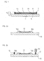
- FIG. 1 is a schematic side sectional view of a first embodiment of the optoelectronic component assembly according to the invention shown.
- the support element 1 is formed in this example as a known circuit board made of FR4 material. Alternatively, however, other materials for the support element 1 into consideration, such as FR5, alumina, glass, etc. ..
- an unhoused component 3 is provided in the illustrated embodiment in the form of a photodetector whose radiation-sensitive surface is oriented away from the carrier element 1.
- a corresponding unhoused light source a so-called.
- Opto-ASIC or other optoelectronic element as optoelectronic device 3 could be used at this point.
- the respective optoelectronic component 3 is connected by means of bonding wires 4a, 4b to the electrical lines in the carrier element 1 or electrically contacted via the bonding wires 4a, 4b in a known manner.
- the material used for the bonding wires 4a, 4b in the present example is gold.
- gold alloys, aluminum, aluminum alloys or copper can be used as bonding wire materials.
- the optoelectronic component 2 is glued in the illustrated embodiment on the Queen element 1; Alternatively, this compound could also be made by alloying, eutectic bonding, anodized bonding, brazing or welding.
- the optoelectronic component arrangement according to the invention comprises a dam 2 arranged on the carrier element 1, which surrounds or circumscribes the component 3 in a closed manner.
- the dam 2 can have a variety of Umlaufgeometrien;
- the dam 2 may surround the structural element 3 in a square manner, but alternatively it is also possible for a rectangular, polygonal or circular embankment course to be provided around the structural element 3.
- the dam 2 has a height h 2 , which is chosen significantly larger than the height h 1 of the component 3 in the present example.
- An essential function of the dam 2 in the device arrangement according to the invention is that it limits the required area on the carrier element 1, which is required for potting the component 3 in the inner area of the dam with encapsulation.
- two potting materials 5, 6 are used for potting, as will be explained in detail below.
- the casting of the component arrangement with the two potting materials 5, 6 serves to protect the component 3 and the bonding wires 4a, 4b against mechanical influences.
- a known black Epoxy galllmasse be provided in the form of a filled epoxy resin, as sold by the company Emerson & Cuming under the type name Amicon 50300 HT .
- epoxy fillers from Dexter Hysol , which are sold under the product designations FP 4451 .
- the dam 2 consists in the present embodiment of a single dam layer, as shown in FIG. 1 is apparent.
- a two- or multi-layer dam structure could also be provided, as described, for example, in German Patent Application No. 100 24 336.3.
- the encapsulation which encapsulates the optoelectronic component 3, arranged in the trough-like dam interior, consists of two different encapsulation materials 5, 6.
- the inner dam area is filled up to the upper edge of the optoelectronic component 3 with a first potting material 5.
- the first potting material 5 in the example shown has a height that corresponds to the height h 1 of the component 3.
- the perineal area is filled up to the upper edge of the optoelectronic component 3 with the first potting material and consequently that the radiation-sensitive or optionally radiation-emitting surface of the optoelectronic component 3 is not substantially covered by the first potting material 5.
- the first potting material 5 is selected such that its thermal expansion coefficient ⁇ VM1 is matched to the thermal expansion coefficients of the bonding wires 4a, 4b ( ⁇ BD ) and of the carrier element 1 ( ⁇ TE ).
- a black Epoxy galmasse is used, which has a thermal expansion coefficient ⁇ VM1 ⁇ 18-19 ppm / K. This is compared to the thermal expansion coefficient ⁇ BD ⁇ 15 ppm / K of the bonding wires 4a, 4b already achieved a very good match when gold is used as the material for the bonding wires 4a, 4b.
- the other materials already mentioned above for the bonding wires 4a, 4b also have coefficients of thermal expansion in the range of .alpha. BD.sup. + (15 ppm / K-25 ppm / K).
- FR4 as the material for the carrier element 1
- Suitable first potting materials 5 are sold for example by the company Emerson & Cuming or Dexter Hysol under the product name Amicon 50500-1 or FP 4450.
- the first potting material 5 and the material of the dam 2 therefore have the same base material in the illustrated embodiment and have only different viscosities. As will be explained later, this choice of material also results in advantages in the course of a possible embodiment of the production method according to the invention.
- the first potting material 5 is further selected such that it has the largest possible surface roughness in the cured state. As a result, a very good adhesion with the overlying material, namely the second potting material 6 can be ensured.
- the second potting material 6 is a commercially available transparent potting material, which is arranged in the dam interior area at least in a window area above the optoelectronic component 3, that is, for example, in the radiation-sensitive region of the photoelement etc. Suitable for the second potting material 6, for example the product marketed by Dexter Hysol under the product name Hysol OS 2800 . Alternatively, the potting materials sold under the product names Hysol OS 1600, Hysol OS 1900, Hysol OS 2902, Hysol OS 4000 or Hysol OS 4110 by the same company would also be usable at this point.
- the second potting material 6 completely fills the dam interior area above the first potting material 5 and the optoelectronic component 3. As already mentioned, however, alternatively only a smaller window area could be filled with it.
- the arrangement according to the invention and the choice of potting materials 5, 6 ensure that the total filling volume in the interior of the dam, which must be filled with the transparent second potting material 6, can be significantly reduced.
- the problems in connection with the thermally induced shearing off of the bonding wires 4a, 4b resulted mainly due to the strongly differing thermal expansion coefficients of transparent potting materials on the one hand and the bonding wires 4a, 4b or of the carrier element 1 on the other hand.
- the reduced fill volume also has the positive effect of reducing the stresses within the device arrangement due to the curing shrinkage process.
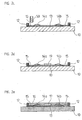
- the unpackaged optoelectronic component 13 is first arranged in the form of an opto-ASIC on the carrier element 10 or the printed circuit board and glued thereto. Furthermore, the optoelectronic component 13 is electrically contacted, which can be done in a known manner via wire bonding and the arrangement of corresponding bonding wires 14a, 14b.
- the dam 12 is applied to the carrier element 10 with the height h 2 , which, as explained above, completely encloses the optoelectronic component 13.
- the corresponding process step is in FIG. 2b illustrated.
- the application of the corresponding dam material is carried out in this example by means of a schematically indicated dispensing needle 50 in the so-called. Dispense technique.
- a dam or frame element designed as an injection molded part could be placed on the carrier element.
- the desired height h 2 of the dam 12 can be defined in the case of application via the dispensing technique by adjusting the speed of the dispensing needle 50, the applied amount of dam material, etc. defined.
- a first potting material 15 is introduced in the dam interior area with the aid of the dispensing needle 50 up to the height h 1 of the component upper edge.
- a first potting material 15 is selected, which consists of the same base material as the dam 12.
- a black, filled epoxy resin or an epoxy filling compound can be used for this purpose.
- the curing of the dam 12 and of the first potting material 15 takes place via a suitable tempering process.
- an additional glass plate 19 is arranged on the radiation-sensitive surface of the component 13 or of the opto-ASIC. This can be like in Figure 2d indicated before filling with the second transparent potting material; Alternatively, however, it is also possible to press the glass plate 19 onto the surface of the component 13 only after the rest of the inner wall of the dam has been filled with the transparent second potting material.
- the arrangement of the glass plate 19 is used in the case of devices 13 with non-passivated active surfaces to protect or seal these surfaces.
- the thickness of the glass plate 19 is selected to be large enough, an additional mechanical protection for the bonding wires 14a, 14b can be ensured.
- the glass plate may of course also have a greater thickness and then slightly protrude from the second potting material.
- the remaining inner dam area is filled by means of the dispensing needle 70 with the second potting material 16 to about the dam top edge, for which, as explained above, a transparent potting material is used.
Description
- Die vorliegende Erfindung betrifft eine optoelektronische Bauelementanordnung. Desweiteren betrifft die vorliegende Erfindung ein Verfahren zur Herstellung einer optoelektronischen Bauelementanordnung.
- Eine optoelektronische Bauelementanordnung ist aus der JP 8-241976 bekannt. Auf einem Trägerelement ist ein als CCD-Chip ausgebildetes optoelektronisches Bauelement angeordnet, das von einem Damm ringförmig umgeben ist. Das Bauelement ist über Bonddrähte mit Leitungen im Trägerelement verbunden und wird derart elektrisch kontaktiert. Im Damm-Innenbereich ist ein Verguss angeordnet, der aus zwei transparenten Vergussmaterialien besteht. Aufgrund thermisch induzierter Spannungen können Risse im Verguss auftreten und ggf. die Bonddrähte beschädigen. Es wird daher vorgeschlagen, in einem ersten Schritt ein erstes transparentes Vergussmaterial in den Damm-Innenbereich einzubringen, dieses thermisch auszuhärten und dabei Luftblasen aus dem Vergussmaterial zu eliminieren. Anschließend wird in einem zweiten Verfahrensschritt eine zweite transparente Vergussmasse in den Damm-Innenbereich eingebracht und wiederum thermisch ausgehärtet, um eventuelle Luftblasen im zweiten Vergussmaterial zu beseitigen. Auf diese Art und Weise lässt sich gewährleisten, dass keine Luftblasen mehr in den beiden Vergussmaterialien enthalten sind. Werden in einer derartigen Bauelementanordnung nunmehr Materialien mit stark voneinander abweichenden thermischen Ausdehnungskoeffizienten verwendet, können unter thermischen Belastungen Bonddraht-Risse auftreten. Deutlich unterschiedliche thermische Ausdehnungskoeffizienten weisen etwa die einerseits verwendeten transparenten Vergussmaterialien bzw. Epoxidharze (α ≈ 50 - 70 ppm/K) und andererseits die eingesetzten Materialien für das Trägerelement bzw. die Bonddrähte (α ≈ 15 - 25 ppm/K) auf.
- Weitere optoelektronische Bauelementanordnungen sind aus der WO 01/24281 A1 bekannt. Die in dieser Druckschrift in Fig. 4 offenbarte Bauelementanordnung sieht hierbei ebenfalls zwei verschiedene Vergussmaterialien vor, die zum einen den Damm-Innebreich ausfüllen und zum anderen die gesamte Bauelementanordnung überdecken. Dadurch wird zwar die thermomechanische Spannungsentlastung des optoelektronischen Bauelements verbessert, jedoch ist aufgrund der Anordnung der beiden Vergussmaterialien nach wie vor erforderlich, dass beide Materialien teiltransparent sind. Dies schränkt die, Wahl optimal angepasster Vergussmaterialien ein, so dass letztlich keine ideale Anpassung in Bezug auf die thermischen Ausdehnungskoeffizienten möglich ist.
- Aus der US 5,861,680 sind verschiedene optoelektronische Bauelementanordnungen bekannt, bei denen jeweils ein optoelektrisches Bauelement auf einem Trägerelement von einem Damm oder Rahmen umgeben ist, wobei das Bauelement über Bonddrähte elektrisch kontaktiert wird. Der Innenbereich des Damms bzw. Rahmens ist mit einem transparenten Vergussmaterial ausgefüllt. Die Beispiele aus den Figuren 1A und 1B unterscheiden sich hierbei lediglich in Bezug auf die Anordnung z.B. auf einer Platine bzw. durch die jeweilige Kontaktierungsmöglichkeit; so offenbart Fig. 1A eine sog. DIP-Anordnung, die zur Durchsteckmontage geeignet ist, in Fig. 1B ist eine LCC-Anordnung gezeigt, welche zur SMD-Bestückung geeignet ist. Ein temperaturbedingtes Beschädigen der Bonddrähte soll gemäß dieser Druckschrift dadurch verhindert werden, dass die Härte des Vergussmaterials während der Fertigung geeignet eingestellt wird.
- Aus der EP 0 632 508 A2 ist eine Photodetektoranordnung mit einem Mehrschichtfilter sowie ein Verfahren zu deren Herstellung bekannt. Bei dem in Figur 12 dargestellten Ausführungsbeispiel ist in einer Vertiefung eines Trägerelements ein Photodetektorelement platziert, welches mittels Bonddrähten kontaktiert wird. Innerhalb der Vertiefung ist ein erstes nichttransparentes Vergussmaterial benachbart zum Photodetektorelement angeordnet, darüber ein zweites transparentes Vergussmaterial. Nachteilig an dieser Anordnung ist insbesondere, dass eine aufwendige formgebende Bearbeitung des Trägerelements nötig ist, um die Vertiefung auszubilden.
- Aufgabe der vorliegenden Erfindung ist es daher, eine optoelektronische Bauelementanordnung sowie ein geeignetes Verfahren zu deren Herstellung anzugeben, worüber sichergestellt ist, dass die zur Kontaktierung des optoelektronischen Baulementes vorgesehenen Bonddrähte auch bei variierenden Temperaturen nicht beschädigt werden.
- Die erste, angegebene Aufgabe wird gelöst durch eine optoelektronische Bauelementanordnung mit den Merkmalen des Anspruches 1.
- Vorteilhafte Ausführungsformen der erfindungsgemäßen optoelektronischen Bauelementanordnung ergeben sich aus den Maßnahmen, die in den von Anspruch 1 abhängigen Patentansprüchen aufgeführt sind:
- Die zweite aufgeführte Aufgabe wird durch ein Verfahren zur Herstellung einer optoelektronischen Bauelementanordnung gemäß den Maßnahmen des Anspruches 9 gelöst.
- Vorteilhafte Ausführungsformen des erfindungsgemäßen Verfahrens ergeben sich aus den Maßnahmen, die in den von Anspruch 9 abhängigen Patentansprüchen aufgeführt sind.
- Erfindungsgemäß wird nunmehr ein erstes Vergussmaterial in den Damm-Innenbereich eingebracht, wobei das erste Vergussmaterial vorteilhafterweise bis zur Oberkante des optoelektronischen Bauelementes reicht. Zumindest in einem räumlich definierten Fensterbereich wird darüber ein transparentes zweites Vergussmaterial eingebracht. Das erste Vergussmaterial wird vorzugsweise unterschiedlich, zum transparenten zweiten Vergussmaterial gewählt. Insbesondere wird bei der Wahl, des ersten Vergussmateriales berücksichtigt, dass dieses einen möglichst niedrigen thermischen Ausdehnungskoeffizienten aufweist, der an den thermischen Ausdehnungskoeffizienten der verwendeten Bonddrähte und des verwendeten Trägerelementes angepasst ist. Auf diese Art und
- Weise lassen sich thermisch induzierte Spannungen im Bereich der Bonddrähte und damit ein unerwünschtes Reissen derselben vermeiden.
- Weiterhin vorteilhaft erweist sich, wenn bei der Wahl des ersten Vergussmateriales ein Material gewählt wird, das im ausgehärteten Zustand eine möglichst rauhe Oberfläche besitzt. Derart ist eine gute Haftung des darüber angeordneten zweiten Vergussmateriales sichergestellt, die zudem gewährleistet, dass es zu keinen thermisch verursachten Verscherungsbewegungen zwischen den beiden Vergussmaterialien kommt, die ggf. die Bonddrähte beschädigen könnten. Bei der Wahl des ersten Vergussmateriales müssen zudem nicht mehr dessen optische Eigenschaften berücksichtigt werden, d.h. die Materialwahl kann allein unter den oben angeführten Optimierungskriterien erfolgen.
- Ein besonderer herstellungstechnischer Vorteil resultiert in einer möglichen Ausführungsform des erfindungsgemäßen Verfahrens, wenn das erste Vergussmaterial und das Damm-Material aus dem im wesentlich gleichen Grundmaterial bestehen und lediglich unterschiedliche Viskositäten besitzen, da dann das erste Vergussmaterial und der Damm im gleichen Arbeitsschritt aufgebracht und ausgehärtet werden können.
- Weitere Vorteile sowie Einzelheiten der vorliegenden Erfindung ergeben sich aus der nachfolgenden Beschreibung von Ausführungsbeispielen anhand der beiliegenden Figuren.
- Dabei zeigt
- Figur 1
- eine schematisierte Schnittansicht eines ersten Ausführungsbeispieles der erfindungsgemäßen optoelektronischen Bauelementanordnung;
- Figur 2a - 2e
- jeweils einen Verfahrensschritt im Rahmen des erfindungsgemäßen Verfahrens zur Herstellung einer zweiten Ausführungsform der erfindungsgemäßen optoelektronischen Bauelementanordnung.
- In
Figur 1 ist eine schematisierte, seitliche Schnittansicht einer ersten Ausführungsform der erfindungsgemäßen optoelektronischen Bauelementanordnung dargestellt. Hierbei sind auf einem Trägerelement 1 die weiteren, nachfolgend zu erläuternden Komponenten der Bauelementanordnung angeordnet. Das Trägerelement 1 ist in diesem Beispiel als bekannte Leiterplatte aus FR4-Material ausgebildet. Alternativ kommen jedoch auch andere Materialien für das Trägerelement 1 in Betracht, wie etwa FR5, Aluminiumoxid, Glas etc.. - Nicht erkennbar sind in
Figur 1 die im Trägerelement 1 verlaufenden Leitungen, die zur elektrischen Kontaktierung des auf dem Trägerelement 1 angeordneten optoelektronischen Bauelementes 3 und eventueller weiterer Bauelemente dienen. Als optoelektronisches Bauelement 3 ist im dargestellten Ausführungsbeispiel ein ungehäustes Bauelement 3 in Form eines Fotodetektors vorgesehen, dessen strahlungsempfindliche Fläche vom Trägerelement 1 weg orientiert ist. Alternativ hierzu könnte auch eine entsprechende ungehäuste Lichtquelle, ein sog. Opto-ASIC oder ein sonstiges Optoelektronik-Element als optoelektronisches Bauelement 3 an dieser Stelle zum Einsatz kommen. - Das jeweilige optoelektronische Bauelement 3 wird mittels Bonddrähten 4a, 4b mit den elektrischen Leitungen im Trägerelement 1 verbunden bzw. über die Bonddrähte 4a, 4b in bekannter Art und Weise elektrisch kontaktiert. Als Material wird für die Bonddrähte 4a, 4b im vorliegenden Beispiel Gold verwendet. Darüberhinaus sind auch Gold-Legierungen, Aluminium, AluminiumLegierungen oder aber Kupfer als Bonddraht-Materialien einsetzbar.
- Das optoelektronische Bauelement 2 ist im dargestellten Ausführungsbeispiel auf dem Trägerlement 1 aufgeklebt; alternativ könnte diese Verbindung auch durch Legieren, Eutektisches Bonden, Anodisiertes Bonden, Löten oder aber Schweißen hergestellt werden.
- Desweiteren umfasst die erfindungsgemäße optoelektronische Bauelementanordnung einen auf dem Trägerelement 1 angeordneten Damm 2, der das Bauelement 3 geschlossen umgibt bzw. umläuft. Der Damm 2 kann verschiedenste Umlaufgeometrien aufweisen; beispielsweise kann der Damm 2 das Bauelement 3 quadratisch umgeben, alternativ kann aber auch ein rechteckförmiger, vieleckförmiger oder runder Dammverlauf um das Bauelement 3 vorgesehen sein.
- Der Damm 2 weist eine Höhe h2 auf, die im vorliegenden Beispiel deutlich größer als die Höhe h1 des Bauelementes 3 gewählt ist. Typische Werte für die Höhen h1, h2 betragen etwa h1 = 450µm und h2= 800µm.
- Eine wesentliche Funktion des Dammes 2 besteht in der erfindungsgemä-ßen Bauelementanordnung darin, dass darüber die benötigte Fläche auf dem Trägerelement 1 begrenzt wird, die zum Vergießen des Bauelementes 3 im Damm-Innenbereich mit einem Verguss erforderlich ist. Erfindungsgemäß werden zum Vergießen zwei Vergussmaterialien 5, 6 verwendet, wie nachfolgend noch detailliert erläutert wird. Das Vergießen der Bauelementanordnung mit der beiden Vergussmaterialien 5, 6 dient zum Schutz des Bauelementes 3 sowie der Bonddrähte 4a, 4b gegenüber mechanischen Einflüssen.
- Als geeignetes Damm-Material kann eine bekannte schwarze Epoxyfüllmasse in Form eines gefüllten Epoxidharzes vorgesehen werden, wie sie von der Firma Emerson & Cuming unter der Typenbezeichnung Amicon 50300 HT vertrieben wird. Alternativ können auch Epoxyfüllmassen der Firma Dexter Hysol verwendet werden, die unter den Produktbezeichnungen FP 4451 vertrieben werden.
- Der Damm 2 besteht im vorliegenden Ausführungsbeispiel aus einer einzigen Dammschicht, wie dies in
Figur 1 ersichtlich ist. Alternativ könnte jedoch auch ein zwei- oder mehrschichtiger Dammaufbau vorgesehen werden, wie dies z.B. in der deutschen Patentanmeldung Nr. 100 24 336.3 beschrieben ist. Desweiteren wäre es alternativ möglich, den Damm 2 als Spritzgussteil auszubilden. - Wesentlich für die vorliegende Erfindung ist nunmehr, dass der im wannenartigen Damm-Innenbereich angeordnete Verguss, der das optoelektronische Bauelement 3 umkapselt, aus zwei verschiedenen Vergussmaterialien 5, 6 besteht. Hierbei ist im dargestellten Beispiel der Damm-Innenbereich bis zur Oberkante des optoelektronischen Bauelementes 3 mit einem ersten Vergussmaterial 5 gefüllt. Das erste Vergussmaterial 5 weist im dargestellten Beispiel demzufolge eine Höhe auf, die der Höhe h1 des Bauelementes 3 entspricht. Grundsätzlich sollte sichergestellt sein, dass der Damm-Innenbereich bis zur Oberkante des optoelektronischen Bauelementes 3 mit dem ersten Vergussmaterial gefüllt ist und demzufolge auch die strahlungsempfindliche oder ggf. strahlungsemittierende Fläche des optoelektronischen Bauelementes 3 nicht wesentlich vom ersten Vergussmaterial 5 bedeckt ist.
- Das erste Vergussmaterial 5 wird erfindungsgemäß derart gewählt, dass dessen thermischer Ausdehnungskoeffizient αVM1 an den thermischen Ausdehnungskoeffizienten der Bonddrähte 4a, 4b (αBD) und des Trägerelementes 1 (αTE) angepasst ist. Hierzu wird beispielsweise eine schwarze Epoxyfüllmasse verwendet, die einen thermischen Ausdehnungskoeffizienten αVM1 ≈ 18 - 19 ppm/K aufweist. Damit ist gegenüber dem thermischen Ausdehnungskoeffizienten αBD ≈ 15 ppm/K der Bonddrähte 4a, 4b bereits eine sehr gute Anpassung erreicht, wenn als Material für die Bonddrähte 4a, 4b Gold verwendet wird. Auch die anderen, oben bereits erwähnten Materialien für die Bonddrähte 4a, 4b weisen thermische Ausdehnungskoeffizienten im Bereich αBD ≈ [15 ppm/K - 25 ppm/K] auf. Ebenso liegt im Fall der Verwendung von FR4 als Material für das Trägerelement 1 eine gute Anpassung an dessen thermischen Ausdehnungskoeffizienten αTE ≈ 15 ppm/K vor. Geeignete erste Vergussmaterialien 5 werden z.B. von den Firma Emerson & Cuming oder Dexter Hysol unter den Produktbezeichnung Amicon 50500-1 bzw. FP 4450 vertrieben.
- Das erste Vergussmaterial 5 und das Material des Dammes 2 weisen in der erläuterten Ausführungsform demzufolge das gleiche Grundmaterial auf und besitzen lediglich unterschiedliche Viskositäten. Wie später noch erläutert wird, resultieren aus dieser Materialwahl auch Vorteile im Verlauf einer möglichen Ausführungsform des erfindungsgemäßen Herstellungsverfahrens.
- Das erste Vergussmaterial 5 wird ferner derart gewählt, dass dieses im ausgehärteten Zustand eine möglichst große Oberflächenrauheit besitzt. Dadurch kann eine sehr gute Haftung mit dem darüber angeordneten Material, nämlich dem zweiten Vergussmaterial 6 sichergestellt werden. Beim zweiten Vergussmaterial 6 handelt es sich um ein handelsübliches transparentes Vergussmaterial, das im Damm-Innenbereich zumindest in einem Fensterbereich oberhalb des optoelektronischen Bauelementes 3 angeordnet ist, also beispielsweise im strahlungsempfindlichen Bereich des Fotoelementes etc.. Als geeignet erweist sich für das zweite Vergussmaterial 6 z.B. das von der Firma Dexter Hysol unter der Produktbezeichnung Hysol OS 2800 vertriebene Produkt. Alternativ wären auch die unter den Produktbezeichnungen Hysol OS 1600, Hysol OS 1900, Hysol OS 2902, Hysol OS 4000 oder Hysol OS 4110 von der gleichen Firma vertriebenen Vergussmaterialien an dieser Stelle verwendbar.
- Im Beispiel der
Figur 1 füllt das zweite Vergussmaterial 6 den Damm-Innenbereich über dem ersten Vergussmaterial 5 und dem optoelektronischen Bauelement 3 vollständig aus. Wie bereits erwähnt, könnte alternativ aber auch lediglich ein kleinerer Fensterbereich damit gefüllt werden. - Durch die erfindungsgemäße Anordnung und Wahl der Vergussmaterialien 5, 6 wird zum einen sichergestelt, dass das Gesamt-Füllvolumen im Damm-Innenbereich, welches mit dem transparenten, zweiten Vergussmaterial 6 gefüllt werden muss, deutlich reduziert werden kann. Wie oben erläutert resultierten die Probleme in Verbindung mit dem thermisch induzierten Abscheren der Bonddrähte 4a, 4b im wesentlichen aufgrund der stark differierenden thermischen Ausdehnungskoeffizienten transparenter Vergussmaterialien einerseits und der Bonddrähte 4a, 4b bzw. des Trägerelementes 1 andererseits. Das verringerte Füllvolumen wirkt sich auch dahingehend positiv aus, dass die auf den Schrumpfungsprozess beim Aushärten zurückgehenden Spannungen innerhalb der Bauelementanordnung reduziert werden. Desweiteren ist aufgrund der rauhen Oberflächenbeschaffenheit des ersten Vergussmateriales 5 gewährleistet, dass eine gute Verzahnung mit dem darüberliegenden zweiten Vergussmaterial 6 resultiert. Dadurch ist ein thermisch bedingtes Abscheren der beiden Vergussmaterialien 5, 6 gegeneinander und damit ein Reissen der Bonddrähte 4a, 4b praktisch nicht mehr möglich.
- Neben der erläuterten ersten Ausführungsform einer optoelektronischen Bauelementanordnung existieren im Rahmen der vorliegenden Erfindung selbstverständlich noch alternative Ausführungsvarianten. Eine zweites Ausführungsbeispiel sei nachfolgend in Verbindung mit den
Figuren 2a - 2e erläutert, anhand der auch eine mögliche Ausführungsform des erfindungsgemäßen Verfahrens beschrieben wird.
In einem ersten Prozessschritt, dargestellt inFigur 2a , wird zunächst das ungehäuste optoelektronische Bauelement 13 in Form eines Opto-ASICs auf dem Trägerelement 10 bzw. der Leiterplatte angeordnet und darauf verklebt. Ferner wird das optoelektronische Bauelement 13 elektrisch kontaktiert, was in bekannter Art und Weise über Drahtbonden und das Anordnen von entsprechenden Bonddrähten 14a, 14b erfolgen kann. - Nachfolgend wird der Damm 12 auf dem Trägerelement 10 mit der Höhe h2 aufgebracht, der wie oben erläutert das optoelektronische Bauelement 13 vollständig umschließt. Der entsprechende Prozessschritt ist in
Figur 2b veranschaulicht. Das Aufbringen des entsprechenden Damm-Materiales erfolgt in diesem Beispiel mit Hilfe einer schematisch angedeuteten Dosiernadel 50 in der sog. Dispense-Technik. Wie bereits erwähnt könnte alternativ auch ein als Spritzgussteil ausgebildeter Damm bzw. Rahmenelement auf das Trägerelement aufgesetzt werden. - Die gewünschte Höhe h2 des Dammes 12 lässt sich im Fall der Aufbringung über die Dispense-Technik durch Abstimmen der Verfahrgeschwindigkeit der Dosiernadel 50, der aufgebrachten Menge des Damm-Materiales etc. definiert einstellen.
- Im anschließenden Prozesschritt, dargestellt in
Figur 2c , wird im Damm-Innenbereich mit Hilfe der Dosiernadel 50 bis zur Höhe h1 der Bauelement-Oberkante ein erstes Vergussmaterial 15 eingebracht. Wie oben erläutert, wird in diesem Ausführungsbeispiel ein erstes Vergussmaterial 15 gewählt, das aus dem gleichen Grundmaterial wie der Damm 12 besteht. Beispielsweise kann hierzu ein schwarzes, gefülltes Epoxidharz bzw. eine Epoxyfüllmasse verwendet werden. Nachfolgend erfolgt über einen einen geeigneten Temperungs-Prozess das Aushärten des Dammes 12 als auch des ersten Vergussmateriales 15. - Im nachfolgenden Verfahrensschritt, der in
Figur 2d dargestellt ist, wird im Unterschied zum ersten erläuterten Ausführungsbeispiel, eine zusätzliche Glasplatte 19 auf der strahlungsempfindlichen Fläche des Bauelementes 13 bzw. des Opto-ASICs angeordnet. Dies kann wie inFigur 2d angedeutet vor dem Auffüllen mit dem zweiten transparenten Vergussmaterial erfolgen; alternativ ist es aber auch möglich, die Glasplatte 19 erst nach dem restlichen Auffüllen des Damm-Innenbereiches mit dem transparenten zweiten Vergussmaterial auf die Oberfläche des Bauelementes 13 anzupressen. - Die Anordnung der Glasplatte 19 dient im Fall von Bauelementen 13 mit nicht-passivierten aktiven Flächen zum Schutz bzw. Versiegeln dieser Flächen. Wenn außerdem die Dicke der Glasplatte 19 groß genug gewählt wird, kann damit ein zusätzlicher mechanischer Schutz für die Bonddrähte 14a, 14b gewährleistet werden. Alternativ zum dargestellten Ausführungsbeispiel kann die Glasplatte selbstverständlich auch eine größere Dicke aufweisen und dann geringfügig aus dem zweiten Vergussmaterial herausragen.
- Im nächsten Verfahrensschritt, dargestellt in
Figur 2e , wird schließlich der verbleibende Damm-Innenbereich mit Hilfe der Dosiernadel 70 mit dem zweiten Vergussmaterial 16 bis etwa zur Damm-Oberkante gefüllt, wozu wie oben erläutert ein transparentes Vergussmaterial verwendet wird.
Claims (14)
- Optoelektronische Bauelementanordnung, bestehend aus- einem Trägerelement (1; 10),- einem auf dem Trägerelement (1; 10) angeordneten optoelektronischen Bauelement (3; 13), das über Bonddrähte (4a, 4b; 14a, 14b) mit Leitungen im Trägerelement (1; 10) verbunden ist,- einem geschlossenen Damm (2; 12) auf dem Trägerelement (1; 10), der das optoelektronische Bauelement (3; 13) umgibt,- einem im Damm-Innenbereich angeordneten Verguss, der das optoelektronische Bauelement (3; 13) umkapselt und zwei Vergussmaterialien (5, 6; 15, 16) umfasst, wobei- der Damm-Innenbereich oberhalb des optoelektronischen Bauelementes (3; 13) zumindest in einem Fensterbereich mit einem transparenten zweiten Vergussmaterial (6; 16) gefüllt ist und- der Damm-Innenbereich bis zur Oberkante des optoelektronischen Bauelementes (3; 13) mit einem ersten nicht-transparenten Vergussmaterial (5; 15) gefüllt ist und- die Bonddrähte (4a, 4b; 14a, 14b) an ihrem trägerelementseitigen Ende vom ersten Vergussmaterial (5; 15) umgeben sind und- das erste Vergussmaterial (5; 15) einen thermischen Ausdehnungskoeffizienten (αVM1) aufweist, welcher an den thermischen Ausdehnungskoeffizienten (αBD) der Bonddrähte (4a, 4b; 14a, 14b) und an den thermischen Ausdehnungskoeffizienten (αTE) des Trägerelementes (1; 10) angepasst ist.
- Optoelektronische Bauelementanordnung nach Anspruch 1, wobei das erste Vergussmaterial (5; 15) einen thermischen Ausdehnungskoeffizienten αVM1 ≈ 18 - 19 ppm/K aufweist.
- Optoelektronische Bauelementanordnung nach Anspruch 1, wobei das erste Vergussmaterial (5; 15) im ausgehärteten Zustand eine große Oberflächenrauheit besitzt.
- Optoelektronische Bauelementanordnung nach Anspruch 1, wobei dass das erste Vergussmaterial (5; 15) eine schwarze Epoxyfüllmasse ist.
- Optoelektronische Bauelementanordnung nach Anspruch 1, wobei das erste Vergussmaterial (5; 15) und das Material des Dammes (2; 12) aus dem gleichen Grundmaterial bestehen und lediglich eine unterschiedliche Viskosität aufweisen.
- Optoelektronische Bauelementanordnung nach Anspruch 1, wobei das zweite Vergussmaterial (6; 16) den Damm-Innenbereich über dem ersten Vergussmaterial (5; 15) und dem optoelektronischen Bauelement (3; 13) vollständig ausfüllt.
- Optoelektronische Bauelementanordnung nach Anspruch 1, wobei das optoelektronische Bauelement (3; 13) als Fotoelement oder Opto-ASIC ausgebildet ist, dessen strahlungsempfindliche Fläche vom Trägerelement (1; 10) weg orientiert ist.
- Optoelektronische Bauelementanordnung nach Anspruch 7, wobei unmittelbar auf der strahlungsempfindlichen Fläche des Fotoelementes oder Opto-ASICs eine Glasplatte (19) angeordnet ist.
- Verfahren zur Herstellung einer optoelektronischen Bauelementanordnung, wobei- auf einem Trägerelement (1; 10) zunächst ein optoelektronisches Bauelement (3; 13) angeordnet und über Bonddrähte (4a, 4b; 14a, 14b) elektrisch kontaktiert wird,- anschließend um das optoelektronische Bauelement (3; 13) ein geschlossener Damm (2; 12) auf dem Trägerelement (1; 10) aufgebracht wird und- in den Damm-Innenbereich ein Verguss aus zwei Verguss-Materialien (5, 6; 15; 16) eingebracht wird, der das optoelektronische Bauelement (3; 13) umkapselt, wobei- der Damm-Innenbereich oberhalb des optoelektronischen Bauelementes (3; 13) zumindest in einem Fensterbereich mit einem transparenten zweiten Vergussmaterial (6; 16) gefüllt wird und- zum Einbringen des Vergusses zunächst ein erstes nichttransparentes Vergussmaterial (5; 15) in den Damm-Innenbereich bis zur Oberkante des optoelektronischen Bauelementes (3; 13) eingebracht wird, wodurch die Bonddrähte (4a, 4b; 14a, 14b) an ihrem trägerelementseitigen Ende vom ersten Vergussmaterial (5; 15) umgeben werden und- dass ein erstes Vergussmaterial (5; 15) gewählt wird, das einen thermischen Ausdehnungskoeffizienten (αVM1) aufweist, welcher an den thermischen Ausdehnungskoeffizienten (αBD) der Bonddrähte (4a, 4b; 14a, 14b) und an den thermischen Ausdehnungskoeffizienten (αTE) des Trägerelementes (1; 10) angepasst ist.
- Verfahren nach Anspruch 9, wobei ein erstes Vergussmaterial (5; 15) gewählt wird, das einen thermischen Ausdehnungskoeffizienten αVM1 ≈ 18 - 19 ppm/K aufweist.
- Verfahren nach Anspruch 9, wobei ein erstes Vergussmaterial (5; 15) gewählt wird, das im ausgehärteten Zustand eine große Oberflächenrauheit besitzt.
- Verfahren nach Anspruch 9, wobei als erstes Vergussmaterial (5; 15) eine schwarze Epoxyfüllmasse gewählt wird.
- Verfahren nach Anspruch 9, wobei das zweite Vergussmaterial (6; 16) in den vollständigen Damm-Innenbereich über dem ersten Vergussmaterial (5; 15) eingebracht wird.
- Verfahren nach Anspruch 9, wobei das optoelektronische Bauelement (3; 13) elektrisch leitend mit Leiterbahnen im Trägerelement (1; 10) verbunden wird.
Applications Claiming Priority (3)
| Application Number | Priority Date | Filing Date | Title |
|---|---|---|---|
| DE10118231A DE10118231A1 (de) | 2001-04-11 | 2001-04-11 | Optoelektronische Baulelmentanordnung und Verfahren zur Herstellun einer oploelektronischen Bauelementanordnung |
| DE10118231 | 2001-04-11 | ||
| PCT/EP2002/003564 WO2002084746A2 (de) | 2001-04-11 | 2002-03-30 | Optoelektronische bauelementanordnung und verfahren zur herstellung einer optoelektronischen bauelementanordnung |
Publications (3)
| Publication Number | Publication Date |
|---|---|
| EP1380056A2 EP1380056A2 (de) | 2004-01-14 |
| EP1380056B1 EP1380056B1 (de) | 2007-05-23 |
| EP1380056B2 true EP1380056B2 (de) | 2014-07-09 |
Family
ID=7681320
Family Applications (1)
| Application Number | Title | Priority Date | Filing Date |
|---|---|---|---|
| EP02732539.8A Expired - Lifetime EP1380056B2 (de) | 2001-04-11 | 2002-03-30 | Optoelektronische bauelementanordnung und verfahren zur herstellung einer optoelektronischen bauelementanordnung |
Country Status (6)
| Country | Link |
|---|---|
| US (1) | US6861683B2 (de) |
| EP (1) | EP1380056B2 (de) |
| JP (1) | JP4369127B2 (de) |
| AT (1) | ATE363132T1 (de) |
| DE (2) | DE10118231A1 (de) |
| WO (1) | WO2002084746A2 (de) |
Families Citing this family (38)
| Publication number | Priority date | Publication date | Assignee | Title |
|---|---|---|---|---|
| US7170188B2 (en) * | 2004-06-30 | 2007-01-30 | Intel Corporation | Package stress management |
| US7161345B2 (en) * | 2004-09-09 | 2007-01-09 | Veris Industries, Llc | Power monitoring system that determines phase using a superimposed signal |
| US7273767B2 (en) * | 2004-12-31 | 2007-09-25 | Carsem (M) Sdn. Bhd. | Method of manufacturing a cavity package |
| US7364945B2 (en) | 2005-03-31 | 2008-04-29 | Stats Chippac Ltd. | Method of mounting an integrated circuit package in an encapsulant cavity |
| US7354800B2 (en) * | 2005-04-29 | 2008-04-08 | Stats Chippac Ltd. | Method of fabricating a stacked integrated circuit package system |
| DE102005021991A1 (de) | 2005-05-09 | 2006-11-16 | Dr. Johannes Heidenhain Gmbh | Optoelektronische Anordnung und Verfahren zu deren Herstellung |
| US7663214B2 (en) * | 2005-07-25 | 2010-02-16 | Kingston Technology Corporation | High-capacity memory card and method of making the same |
| WO2007012992A1 (en) * | 2005-07-28 | 2007-02-01 | Nxp B.V. | A package and manufacturing method for a microelectronic component |
| US7723146B2 (en) * | 2006-01-04 | 2010-05-25 | Stats Chippac Ltd. | Integrated circuit package system with image sensor system |
| US7456088B2 (en) | 2006-01-04 | 2008-11-25 | Stats Chippac Ltd. | Integrated circuit package system including stacked die |
| US7768125B2 (en) | 2006-01-04 | 2010-08-03 | Stats Chippac Ltd. | Multi-chip package system |
| US7750482B2 (en) | 2006-02-09 | 2010-07-06 | Stats Chippac Ltd. | Integrated circuit package system including zero fillet resin |
| US8704349B2 (en) | 2006-02-14 | 2014-04-22 | Stats Chippac Ltd. | Integrated circuit package system with exposed interconnects |
| US20080122122A1 (en) * | 2006-11-08 | 2008-05-29 | Weng Fei Wong | Semiconductor package with encapsulant delamination-reducing structure and method of making the package |
| CA2609619A1 (en) | 2007-09-10 | 2009-03-10 | Veris Industries, Llc | Status indicator |
| CA2609611A1 (en) * | 2007-09-10 | 2009-03-10 | Veris Industries, Llc | Split core status indicator |
| CA2609629A1 (en) * | 2007-09-10 | 2009-03-10 | Veris Industries, Llc | Current switch with automatic calibration |
| US8212548B2 (en) | 2008-06-02 | 2012-07-03 | Veris Industries, Llc | Branch meter with configurable sensor strip arrangement |
| US8421639B2 (en) | 2008-11-21 | 2013-04-16 | Veris Industries, Llc | Branch current monitor with an alarm |
| US8421443B2 (en) | 2008-11-21 | 2013-04-16 | Veris Industries, Llc | Branch current monitor with calibration |
| US9335352B2 (en) * | 2009-03-13 | 2016-05-10 | Veris Industries, Llc | Branch circuit monitor power measurement |
| US10006948B2 (en) | 2011-02-25 | 2018-06-26 | Veris Industries, Llc | Current meter with voltage awareness |
| US9146264B2 (en) | 2011-02-25 | 2015-09-29 | Veris Industries, Llc | Current meter with on board memory |
| US9329996B2 (en) | 2011-04-27 | 2016-05-03 | Veris Industries, Llc | Branch circuit monitor with paging register |
| US9250308B2 (en) | 2011-06-03 | 2016-02-02 | Veris Industries, Llc | Simplified energy meter configuration |
| US9410552B2 (en) | 2011-10-05 | 2016-08-09 | Veris Industries, Llc | Current switch with automatic calibration |
| CN102931178A (zh) * | 2012-07-30 | 2013-02-13 | 易美芯光(北京)科技有限公司 | 一种新型led集成光源封装结构 |
| US10242969B2 (en) * | 2013-11-12 | 2019-03-26 | Infineon Technologies Ag | Semiconductor package comprising a transistor chip module and a driver chip module and a method for fabricating the same |
| US9196510B2 (en) | 2013-11-12 | 2015-11-24 | Infineon Technologies Ag | Semiconductor package comprising two semiconductor modules and laterally extending connectors |
| US10408911B2 (en) | 2015-12-28 | 2019-09-10 | Veris Industries, Llc | Network configurable system for a power meter |
| US10371721B2 (en) | 2015-12-28 | 2019-08-06 | Veris Industries, Llc | Configuration system for a power meter |
| US10371730B2 (en) | 2015-12-28 | 2019-08-06 | Veris Industries, Llc | Branch current monitor with client level access |
| US10274572B2 (en) | 2015-12-28 | 2019-04-30 | Veris Industries, Llc | Calibration system for a power meter |
| CN109219892A (zh) * | 2016-07-08 | 2019-01-15 | 住友化学株式会社 | 紫外线发光半导体器件及其制造方法 |
| US11215650B2 (en) | 2017-02-28 | 2022-01-04 | Veris Industries, Llc | Phase aligned branch energy meter |
| US11193958B2 (en) | 2017-03-03 | 2021-12-07 | Veris Industries, Llc | Non-contact voltage sensor |
| US10705126B2 (en) | 2017-05-19 | 2020-07-07 | Veris Industries, Llc | Energy metering with temperature monitoring |
| CN111176480A (zh) * | 2019-12-06 | 2020-05-19 | 深圳市鸿合创新信息技术有限责任公司 | 一种触控显示屏及其制备方法、触控装置 |
Family Cites Families (11)
| Publication number | Priority date | Publication date | Assignee | Title |
|---|---|---|---|---|
| JPS5834681A (ja) * | 1981-08-26 | 1983-03-01 | Hitachi Ltd | 固体撮像装置 |
| DE3732075A1 (de) * | 1987-09-23 | 1989-04-06 | Siemens Ag | Hermetisch dichtes glas-metallgehaeuse fuer halbleiterbauelemente und verfahren zu dessen herstellung |
| JP3242495B2 (ja) * | 1993-07-01 | 2001-12-25 | シャープ株式会社 | 多層膜フィルタ付き受光素子及びその製造方法 |
| JP3168859B2 (ja) | 1995-03-06 | 2001-05-21 | 日本ケミコン株式会社 | Ccdモジュールの樹脂封止方法 |
| DE19509262C2 (de) | 1995-03-15 | 2001-11-29 | Siemens Ag | Halbleiterbauelement mit Kunststoffumhüllung und Verfahren zu dessen Herstellung |
| US5962810A (en) | 1997-09-09 | 1999-10-05 | Amkor Technology, Inc. | Integrated circuit package employing a transparent encapsulant |
| DE19755734A1 (de) * | 1997-12-15 | 1999-06-24 | Siemens Ag | Verfahren zur Herstellung eines oberflächenmontierbaren optoelektronischen Bauelementes |
| DE19803936A1 (de) | 1998-01-30 | 1999-08-05 | Patent Treuhand Ges Fuer Elektrische Gluehlampen Mbh | Ausdehnungskompensiertes optoelektronisches Halbleiter-Bauelement, insbesondere UV-emittierende Leuchtdiode und Verfahren zu seiner Herstellung |
| DE19947044B9 (de) * | 1999-09-30 | 2007-09-13 | Osram Opto Semiconductors Gmbh | Oberflächenmontierbares optoelektronisches Bauelement mit Reflektor und Verfahren zur Herstellung desselben |
| DE10023353A1 (de) | 2000-05-12 | 2001-11-29 | Osram Opto Semiconductors Gmbh | Optoelektronisches Bauelement und Verfahren zur Herstellung |
| DE10024336A1 (de) | 2000-05-17 | 2001-11-22 | Heidenhain Gmbh Dr Johannes | Bauelementanordnung und Verfahren zur Herstellung einer Bauelementanordnung |
-
2001
- 2001-04-11 DE DE10118231A patent/DE10118231A1/de not_active Withdrawn
-
2002
- 2002-03-30 AT AT02732539T patent/ATE363132T1/de not_active IP Right Cessation
- 2002-03-30 DE DE50210203T patent/DE50210203D1/de not_active Expired - Lifetime
- 2002-03-30 US US10/474,953 patent/US6861683B2/en not_active Expired - Fee Related
- 2002-03-30 EP EP02732539.8A patent/EP1380056B2/de not_active Expired - Lifetime
- 2002-03-30 WO PCT/EP2002/003564 patent/WO2002084746A2/de active IP Right Grant
- 2002-03-30 JP JP2002581589A patent/JP4369127B2/ja not_active Expired - Fee Related
Also Published As
| Publication number | Publication date |
|---|---|
| WO2002084746A3 (de) | 2003-10-30 |
| ATE363132T1 (de) | 2007-06-15 |
| WO2002084746A2 (de) | 2002-10-24 |
| JP2004528713A (ja) | 2004-09-16 |
| DE10118231A1 (de) | 2002-10-17 |
| US20040150064A1 (en) | 2004-08-05 |
| EP1380056B1 (de) | 2007-05-23 |
| EP1380056A2 (de) | 2004-01-14 |
| JP4369127B2 (ja) | 2009-11-18 |
| DE50210203D1 (de) | 2007-07-05 |
| US6861683B2 (en) | 2005-03-01 |
Similar Documents
| Publication | Publication Date | Title |
|---|---|---|
| EP1380056B2 (de) | Optoelektronische bauelementanordnung und verfahren zur herstellung einer optoelektronischen bauelementanordnung | |
| EP1547166B1 (de) | Lichtquellenmodul sowie verfahren zu dessen herstellung | |
| EP1022787B1 (de) | Verfahren zum Herstellen eines oberflächenmontierbaren Opto-Bauelements und oberflächenmontierbares Opto-Bauelement | |
| EP0809304B1 (de) | Optoelektronischer Wandler und dessen Herstellungsverfahren | |
| DE19518753B4 (de) | Halbleitervorrichtung und Verfahren zu ihrer Herstellung | |
| DE102005034011B4 (de) | Halbleiterbauteil für Hochfrequenzen über 10 GHz und Verfahren zur Herstellung desselben | |
| EP1269450B1 (de) | Bauelement mit beschriftung | |
| EP1717871B1 (de) | Oberflächenmontierbares optoelektronisches Bauelement | |
| EP2606510B1 (de) | Verfahren zur herstellung zumindest eines optoelektronischen halbleiterbauelements | |
| EP1602625A1 (de) | Halbleitermodul mit einem Halbleiter-Sensorchip und einem Kunststoffgehäuse sowie Verfahren zu dessen Herstellung | |
| DE3937996A1 (de) | Verfahren zur herstellung von halbleiteranordnungen | |
| DE102011003195B4 (de) | Bauteil und Verfahren zum Herstellen eines Bauteils | |
| DE102009001969A1 (de) | Sensormodul | |
| DE102006033222B4 (de) | Modul mit flachem Aufbau und Verfahren zur Bestückung | |
| EP1287558B1 (de) | Bauelementanordnung und verfahren zur herstellung einer bauelementanordnung | |
| DE3810899C2 (de) | ||
| EP0243637B1 (de) | Leistungshalbleitermodul | |
| DE102019127007A1 (de) | Stapel elektrischer bauelemente und verfahren zur herstellung desselben | |
| EP2260511B1 (de) | Bauelementanordnung und verfahren zur herstellung einer bauelementanordnung | |
| DE102014116080A1 (de) | Optoelektronisches Bauelement und Verfahren zu seiner Herstellung | |
| WO2022248570A1 (de) | Halbleiterbauelement und verfahren zur herstellung eines halbleiterbauelements | |
| DE102006015241A1 (de) | Halbleiterbauteil mit einem Kunststoffgehäuse und teilweise in Kunststoff eingebetteten Außenkontakten sowie Verfahren zur Herstellung des Halbleiterbauteils | |
| EP1466364B1 (de) | Nutzen für elektronische bauteile sowie verfahren zu dessen herstellung | |
| DE10014299B4 (de) | Chipverbund und Verfahren zu dessen Herstellung | |
| WO2023036975A1 (de) | Optoelektronische vorrichtung und verfahren zur herstellung |
Legal Events
| Date | Code | Title | Description |
|---|---|---|---|
| PUAI | Public reference made under article 153(3) epc to a published international application that has entered the european phase |
Free format text: ORIGINAL CODE: 0009012 |
|
| AK | Designated contracting states |
Kind code of ref document: A2 Designated state(s): AT BE CH CY DE DK ES FI FR GB GR IE IT LI LU MC NL PT SE TR |
|
| 17P | Request for examination filed |
Effective date: 20040503 |
|
| 17Q | First examination report despatched |
Effective date: 20061002 |
|
| GRAP | Despatch of communication of intention to grant a patent |
Free format text: ORIGINAL CODE: EPIDOSNIGR1 |
|
| GRAS | Grant fee paid |
Free format text: ORIGINAL CODE: EPIDOSNIGR3 |
|
| GRAA | (expected) grant |
Free format text: ORIGINAL CODE: 0009210 |
|
| AK | Designated contracting states |
Kind code of ref document: B1 Designated state(s): AT BE CH CY DE DK ES FI FR GB GR IE IT LI LU MC NL PT SE TR |
|
| PG25 | Lapsed in a contracting state [announced via postgrant information from national office to epo] |
Ref country code: FI Free format text: LAPSE BECAUSE OF FAILURE TO SUBMIT A TRANSLATION OF THE DESCRIPTION OR TO PAY THE FEE WITHIN THE PRESCRIBED TIME-LIMIT Effective date: 20070523 |
|
| REG | Reference to a national code |
Ref country code: GB Ref legal event code: FG4D Free format text: NOT ENGLISH |
|
| GBT | Gb: translation of ep patent filed (gb section 77(6)(a)/1977) |
Effective date: 20070523 |
|
| REG | Reference to a national code |
Ref country code: CH Ref legal event code: EP |
|
| REG | Reference to a national code |
Ref country code: IE Ref legal event code: FG4D Free format text: LANGUAGE OF EP DOCUMENT: GERMAN |
|
| REF | Corresponds to: |
Ref document number: 50210203 Country of ref document: DE Date of ref document: 20070705 Kind code of ref document: P |
|
| PG25 | Lapsed in a contracting state [announced via postgrant information from national office to epo] |
Ref country code: SE Free format text: LAPSE BECAUSE OF FAILURE TO SUBMIT A TRANSLATION OF THE DESCRIPTION OR TO PAY THE FEE WITHIN THE PRESCRIBED TIME-LIMIT Effective date: 20070823 |
|
| PG25 | Lapsed in a contracting state [announced via postgrant information from national office to epo] |
Ref country code: ES Free format text: LAPSE BECAUSE OF FAILURE TO SUBMIT A TRANSLATION OF THE DESCRIPTION OR TO PAY THE FEE WITHIN THE PRESCRIBED TIME-LIMIT Effective date: 20070903 |
|
| NLV1 | Nl: lapsed or annulled due to failure to fulfill the requirements of art. 29p and 29m of the patents act | ||
| REG | Reference to a national code |
Ref country code: IE Ref legal event code: FD4D |
|
| PG25 | Lapsed in a contracting state [announced via postgrant information from national office to epo] |
Ref country code: DK Free format text: LAPSE BECAUSE OF FAILURE TO SUBMIT A TRANSLATION OF THE DESCRIPTION OR TO PAY THE FEE WITHIN THE PRESCRIBED TIME-LIMIT Effective date: 20070523 Ref country code: NL Free format text: LAPSE BECAUSE OF FAILURE TO SUBMIT A TRANSLATION OF THE DESCRIPTION OR TO PAY THE FEE WITHIN THE PRESCRIBED TIME-LIMIT Effective date: 20070523 Ref country code: IE Free format text: LAPSE BECAUSE OF FAILURE TO SUBMIT A TRANSLATION OF THE DESCRIPTION OR TO PAY THE FEE WITHIN THE PRESCRIBED TIME-LIMIT Effective date: 20070523 Ref country code: PT Free format text: LAPSE BECAUSE OF FAILURE TO SUBMIT A TRANSLATION OF THE DESCRIPTION OR TO PAY THE FEE WITHIN THE PRESCRIBED TIME-LIMIT Effective date: 20071023 |
|
| PLBI | Opposition filed |
Free format text: ORIGINAL CODE: 0009260 |
|
| PLAX | Notice of opposition and request to file observation + time limit sent |
Free format text: ORIGINAL CODE: EPIDOSNOBS2 |
|
| 26 | Opposition filed |
Opponent name: SICK STEGMANN GMBH Effective date: 20080214 |
|
| PG25 | Lapsed in a contracting state [announced via postgrant information from national office to epo] |
Ref country code: GR Free format text: LAPSE BECAUSE OF FAILURE TO SUBMIT A TRANSLATION OF THE DESCRIPTION OR TO PAY THE FEE WITHIN THE PRESCRIBED TIME-LIMIT Effective date: 20070824 |
|
| PLBB | Reply of patent proprietor to notice(s) of opposition received |
Free format text: ORIGINAL CODE: EPIDOSNOBS3 |
|
| BERE | Be: lapsed |
Owner name: DR. JOHANNES HEIDENHAIN G.M.B.H. Effective date: 20080331 |
|
| PG25 | Lapsed in a contracting state [announced via postgrant information from national office to epo] |
Ref country code: MC Free format text: LAPSE BECAUSE OF NON-PAYMENT OF DUE FEES Effective date: 20080331 |
|
| REG | Reference to a national code |
Ref country code: CH Ref legal event code: PL |
|
| PG25 | Lapsed in a contracting state [announced via postgrant information from national office to epo] |
Ref country code: LI Free format text: LAPSE BECAUSE OF NON-PAYMENT OF DUE FEES Effective date: 20080331 Ref country code: CH Free format text: LAPSE BECAUSE OF NON-PAYMENT OF DUE FEES Effective date: 20080331 |
|
| PG25 | Lapsed in a contracting state [announced via postgrant information from national office to epo] |
Ref country code: BE Free format text: LAPSE BECAUSE OF NON-PAYMENT OF DUE FEES Effective date: 20080331 |
|
| PG25 | Lapsed in a contracting state [announced via postgrant information from national office to epo] |
Ref country code: CY Free format text: LAPSE BECAUSE OF FAILURE TO SUBMIT A TRANSLATION OF THE DESCRIPTION OR TO PAY THE FEE WITHIN THE PRESCRIBED TIME-LIMIT Effective date: 20070523 |
|
| PG25 | Lapsed in a contracting state [announced via postgrant information from national office to epo] |
Ref country code: AT Free format text: LAPSE BECAUSE OF NON-PAYMENT OF DUE FEES Effective date: 20080330 |
|
| APAH | Appeal reference modified |
Free format text: ORIGINAL CODE: EPIDOSCREFNO |
|
| APBM | Appeal reference recorded |
Free format text: ORIGINAL CODE: EPIDOSNREFNO |
|
| APBP | Date of receipt of notice of appeal recorded |
Free format text: ORIGINAL CODE: EPIDOSNNOA2O |
|
| APBQ | Date of receipt of statement of grounds of appeal recorded |
Free format text: ORIGINAL CODE: EPIDOSNNOA3O |
|
| PG25 | Lapsed in a contracting state [announced via postgrant information from national office to epo] |
Ref country code: LU Free format text: LAPSE BECAUSE OF NON-PAYMENT OF DUE FEES Effective date: 20080330 |
|
| PG25 | Lapsed in a contracting state [announced via postgrant information from national office to epo] |
Ref country code: TR Free format text: LAPSE BECAUSE OF FAILURE TO SUBMIT A TRANSLATION OF THE DESCRIPTION OR TO PAY THE FEE WITHIN THE PRESCRIBED TIME-LIMIT Effective date: 20070523 |
|
| APBU | Appeal procedure closed |
Free format text: ORIGINAL CODE: EPIDOSNNOA9O |
|
| RIC2 | Information provided on ipc code assigned after grant |
Ipc: H01L 33/52 20100101ALI20140327BHEP Ipc: H01L 31/0203 20140101AFI20140327BHEP |
|
| PGFP | Annual fee paid to national office [announced via postgrant information from national office to epo] |
Ref country code: IT Payment date: 20140327 Year of fee payment: 13 Ref country code: FR Payment date: 20140319 Year of fee payment: 13 |
|
| PUAH | Patent maintained in amended form |
Free format text: ORIGINAL CODE: 0009272 |
|
| STAA | Information on the status of an ep patent application or granted ep patent |
Free format text: STATUS: PATENT MAINTAINED AS AMENDED |
|
| PGFP | Annual fee paid to national office [announced via postgrant information from national office to epo] |
Ref country code: GB Payment date: 20140319 Year of fee payment: 13 |
|
| 27A | Patent maintained in amended form |
Effective date: 20140709 |
|
| AK | Designated contracting states |
Kind code of ref document: B2 Designated state(s): AT BE CH CY DE DK ES FI FR GB GR IE IT LI LU MC NL PT SE TR |
|
| REG | Reference to a national code |
Ref country code: DE Ref legal event code: R102 Ref document number: 50210203 Country of ref document: DE |
|
| REG | Reference to a national code |
Ref country code: DE Ref legal event code: R102 Ref document number: 50210203 Country of ref document: DE Effective date: 20140709 |
|
| GBPC | Gb: european patent ceased through non-payment of renewal fee |
Effective date: 20150330 |
|
| PG25 | Lapsed in a contracting state [announced via postgrant information from national office to epo] |
Ref country code: IT Free format text: LAPSE BECAUSE OF NON-PAYMENT OF DUE FEES Effective date: 20150330 |
|
| REG | Reference to a national code |
Ref country code: FR Ref legal event code: ST Effective date: 20151130 |
|
| PG25 | Lapsed in a contracting state [announced via postgrant information from national office to epo] |
Ref country code: GB Free format text: LAPSE BECAUSE OF NON-PAYMENT OF DUE FEES Effective date: 20150330 |
|
| PG25 | Lapsed in a contracting state [announced via postgrant information from national office to epo] |
Ref country code: FR Free format text: LAPSE BECAUSE OF NON-PAYMENT OF DUE FEES Effective date: 20150331 |
|
| PGFP | Annual fee paid to national office [announced via postgrant information from national office to epo] |
Ref country code: DE Payment date: 20190321 Year of fee payment: 18 |
|
| REG | Reference to a national code |
Ref country code: DE Ref legal event code: R119 Ref document number: 50210203 Country of ref document: DE |
|
| PG25 | Lapsed in a contracting state [announced via postgrant information from national office to epo] |
Ref country code: DE Free format text: LAPSE BECAUSE OF NON-PAYMENT OF DUE FEES Effective date: 20201001 |