EP1379937B1 - Reset circuit and method therefor - Google Patents
Reset circuit and method therefor Download PDFInfo
- Publication number
- EP1379937B1 EP1379937B1 EP02724495A EP02724495A EP1379937B1 EP 1379937 B1 EP1379937 B1 EP 1379937B1 EP 02724495 A EP02724495 A EP 02724495A EP 02724495 A EP02724495 A EP 02724495A EP 1379937 B1 EP1379937 B1 EP 1379937B1
- Authority
- EP
- European Patent Office
- Prior art keywords
- reset
- clock
- signal
- module
- circuit
- Prior art date
- Legal status (The legal status is an assumption and is not a legal conclusion. Google has not performed a legal analysis and makes no representation as to the accuracy of the status listed.)
- Expired - Lifetime
Links
Images


Classifications
-
- G—PHYSICS
- G06—COMPUTING OR CALCULATING; COUNTING
- G06F—ELECTRIC DIGITAL DATA PROCESSING
- G06F1/00—Details not covered by groups G06F3/00 - G06F13/00 and G06F21/00
- G06F1/24—Resetting means
Definitions
- the present device relates generally to electronic systems and, more particularly, to electronic systems and components exhibiting non-analogous reset strategies.
- modules To contain and potentially shorten the design and development cycle time for large-scale systems, previously designed components, or modules, are commonly used. Such modules, having been designed for systems having differing reset requirements, often have differing clock and timing constraints. Some modules, for example, employ an asynchronous reset scheme, a synchronous reset scheme or a mix of both. Others employ a positive-edge-triggered clocking scheme, a negative-edge-triggered clocking scheme, a level sensitive scheme, a multi-phased scheme, and so on. In like manner, the convention used for resetting each module may differ. For each module, the reset strategy employed introduces timing constraints relative to the particular clocking scheme employed.
- timing constraints include: a synchronous reset must arrive at the module for a specified duration before the active edge of the clock and/or be held at its active state for a specified duration after the clock edge; an asynchronous reset should not be released in close proximity to a change of clock state in a level sensitive clocking design; a reset signal should not be asserted, or de-asserted, in close proximity to an assertion or desertion of a set signal; the release of a reset signal is advantageously effected about simultaneously for all modules; and so on. From a systems viewpoint, the varying reset and clocking strategies produce a combinatorial complex set of design constraints.
- a solution for ensuring that all resets are executed before a system is restarted is provided by PCT patent application WO00/72122 , which discloses a reset module operating in conjunction with a system clock to provide a combination of reset and clock assertions that can be relied upon to reset conventional processing modules having a variety of rest architectures.
- a reset command initiates the assertion of the reset signal and an activation of all clocks at the system level. After a predetermined number of clock cycles, the system level clocks are deactivated, and then the reset signal is de-asserted. By providing multiple clock cycles with the reset signal asserted, processing modules having either asynchronous and synchronous reset will be reset. By disabling the clocks before the de-asserting the reset signal, the likelihood of a timing hazard caused by an interaction of the reset signal and the clocking signal is reduced or eliminated.
- the present invention makes possible a reset circuit that is modular, scaleable, straightforward to implement, allows for simple and safe physical design implementation, and addresses problems stated in the Background hereinabove.
- the present invention is exemplified in a number of implementations and applications, some of which are summarized below.
- a reset circuit is adapted to reset a plurality of circuit modules in a manner that addresses problems including those discussed in the Background hereinabove.
- the reset circuit includes a reset module adapted to generate a reset signal, a clock module and a plurality of synchronization modules.
- the clock module has an external clock reference and at least one clock module output for each of the plurality of circuit modules.
- a reset clock signal is provided to each of the circuit modules via the clock module outputs in response to the generated reset signal.
- the frequency of the clock module is selectable to an external clock reference.
- Each synchronization module is coupled to one of the plurality of circuit modules and has a reset input port coupled to the reset module and a clock input port coupled to one of the clock module outputs.
- the synchronization modules are adapted to synchronize the reset signal to the reset clock signal and to provide the synchronized reset signal to reset each circuit module.
- the circuit modules are adapted to enable internal resets in response to a reset signal.
- a plurality of circuit modules adapted to enable internal resets in response to a reset signal are reset using a method that addresses problems including those discussed in the Background hereinabove.
- a reset signal is generated, and a reset clock signal having a frequency of an external clock reference is sent to each circuit module in response to the generated reset signal.
- the reset signal is synchronized to the reset clock signal for each circuit module, and the synchronized reset signal is to reset each circuit module. When the reset is disabled, each circuit module releases its internal reset almost simultaneously.
- the present invention is believed to be applicable to a variety of different types of electronic devices, and has been found to be particularly suited for use in connection with devices exhibiting non-analogous reset strategies. While the present invention is not limited to such devices, an appreciation of various aspects of the invention is best gained through a discussion of various examples using this application.
- a reset method and system are used to effect a reset at a plurality of circuit modules (e.g., peripheral devices).
- the system includes a reset signal generator coupled to a clock module and to each of the plurality of circuit modules.
- the clock module is coupled to an external clock reference and to each of the circuit modules via clock outputs for the circuit modules.
- a reset clock signal having the reference clock frequency is sent to each of the circuit modules via the clock outputs.
- Each of the circuit modules includes a synchronization module adapted to synchronize the reset signal among all circuit modules using the clock signal received from the clock module.
- the clock module holds the reset clock signal for a selected amount of time, and then releases the signal from the external clock.
- the reset signals are then simultaneously released at each of the circuit modules.
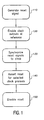
- FIG. 1 is a flow diagram showing a method for resetting a circuit, according to another example embodiment of the present invention.
- a reset signal is generated, and the signal is provided to a clock module and to two or more circuit modules. All clock outputs from the clock module are enabled at a reference clock frequency at block 120.
- the clock outputs are received at each circuit module and used to synchronize the reset signal among the circuit modules.
- the reset is asserted for a selected number of clock periods at block 140, and the reset is disabled after the selected number of clock periods has been reached at block 150, effecting the simultaneous de-assertion of the reset at each circuit module.
- FIG. 2 shows a timing diagram for an electronic system, according to another example embodiment of the present invention.
- Module clock cycles are shown as curve 210, and at clock cycle 212, power Vdd (curve 220) is applied to the system.
- An external reset input, reset_in_n is asserted, shown at curve 230, and held for 1ms.
- the reset input causes assertion of a peripheral reset, peri_rst_n, to the clock module and the circuit modules, shown as curve 240.
- peri_rst_n When peri_rst_n is asserted, the clock module enables an external clock on module clock outputs to the circuit modules, or peripheral devices.
- the external clock is used to apply a synchronized internal reset, mod int_rst_n, at each circuit module, shown by curve 250, using the peri_rst_n signal and the external clock signal.
- the reset_in_n signal is de-asserted at node 232
- the peri_rst_n signal is subsequently de-asserted after one clock cycle at node 242.
- All circuit modules release their internal resets synchronously, or nearly simultaneously, at node 252, which improves the ability to effect a safe transfer to system boot.
- the external clock remains asserted for a selected period, and the clock module then switches to a functional clock for each module after the reset has been released.
- the functional clock may, for example, include a clock signal having a particular frequency and phase related to requirements at each circuit module and overall system timing constraints.
- the selected period for which the external clock is asserted is effected via a register in the clock module that is programmed to hold the external clock for a number of clock cycles.
- the reset_in_n signal is de-asserted
- software in the register operates to switch the clocks from the reference clock to the functional clocks for each circuit module.
- the switch is effected after a number of clock cycles that allows the internal resets to be released before the switch is made.
- the internal reset at each circuit module is released two clock cycles after peri_rst_n is de-asserted.
- the software uses at least two clock cycles to switch from the reference clock to the functional clocks, and ensures that the internal resets are synchronously released using the external clock reference.
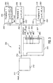
- FIG. 3 shows one such circuit arrangement 300, according to another example embodiment of the present invention.
- the circuit arrangement includes a reset signal generator 310 that is adapted to send a reset signal 314 to a clock module 320 and to peripheral device 1 (item 330), peripheral device 2 (item 332) and peripheral device N (item 334) in response to an input signal 312.
- the clock module 320 includes clock outputs clk1 (item 322), clk2 (item 324), clk3 (item 326) and clkn (item 327) adapted to send a clock signal to each of the peripheral devices.
- FIG. 3 shows three peripheral devices and four clock outputs, the system 300 is adaptable to accommodate additional peripheral devices up to an "N" number of devices, as well as clock outputs for each of the peripheral devices, as indicated by dashed lines.
- Each of the peripheral devices 330, 332 and 334 include synchronization modules 340, 342 and 344, respectively, each having at least one input port adapted to receive the clock outputs, and an input port adapted to receive the reset signal 314.
- Synchronization module 340 receives clock output clk1 and clk2;
- module 342 receives clock output clk3 and
- module 344 receives clock output clkn.
- the synchronization modules use the clock outputs and the reset signal to generate internal reset signals 350, 351, 352 and 353.
- Each internal reset signal is synchronized such that each peripheral device is reset using the same clock input, and thus, each device is released from reset nearly simultaneously when the reset is disabled.
- FIG. 4A and FIG. 4B show example synchronizers adapted to be used in connection with a reset circuit, such as that described in connection with FIG. 3 , according to another example embodiment of the present invention.
- the synchronizer 410 in FIG. 4A is adapted to generate a reset signal asynchronously
- the synchronizer 460 in FIG. 4B is adapted to generate a reset signal synchronously. Both devices are adapted to effect synchronous de-assertion of a reset at a peripheral device.
- reset input signal 414 is received at flip-flop 420 and at AND gate 440.
- a clock signal 416 cycles the flip-flop 420 and the reset input signal is provided to flip-flop 430.
- the clock signal 416 cycles flip-flop 430, and the reset input signal from the flip-flop is provided to AND gate 440, which in turn provides an internal reset signal 418 to the peripheral device for which the synchronizer is used.
- synchronizer 460 receives a reset input signal 464 at flip-flop 470, which cycles according to a clock signal 466.
- the reset signal is provided to flip-flop 480, which is also responsive to the clock signal 466.
- Flip-flop 480 is cycled and provides an internal reset signal 468 to the peripheral device for which the synchronizer is used.
Landscapes
- Engineering & Computer Science (AREA)
- Theoretical Computer Science (AREA)
- Physics & Mathematics (AREA)
- General Engineering & Computer Science (AREA)
- General Physics & Mathematics (AREA)
- Electronic Switches (AREA)
- Debugging And Monitoring (AREA)
Applications Claiming Priority (3)
| Application Number | Priority Date | Filing Date | Title |
|---|---|---|---|
| US826570 | 2001-04-05 | ||
| US09/826,570 US6529053B2 (en) | 2001-04-05 | 2001-04-05 | Reset circuit and method therefor |
| PCT/IB2002/001096 WO2002082246A2 (en) | 2001-04-05 | 2002-04-05 | Reset circuit and method therefor |
Publications (2)
| Publication Number | Publication Date |
|---|---|
| EP1379937A2 EP1379937A2 (en) | 2004-01-14 |
| EP1379937B1 true EP1379937B1 (en) | 2010-12-29 |
Family
ID=25246920
Family Applications (1)
| Application Number | Title | Priority Date | Filing Date |
|---|---|---|---|
| EP02724495A Expired - Lifetime EP1379937B1 (en) | 2001-04-05 | 2002-04-05 | Reset circuit and method therefor |
Country Status (6)
| Country | Link |
|---|---|
| US (1) | US6529053B2 (enExample) |
| EP (1) | EP1379937B1 (enExample) |
| JP (1) | JP4149268B2 (enExample) |
| AT (1) | ATE493696T1 (enExample) |
| DE (1) | DE60238750D1 (enExample) |
| WO (1) | WO2002082246A2 (enExample) |
Families Citing this family (9)
| Publication number | Priority date | Publication date | Assignee | Title |
|---|---|---|---|---|
| US6611158B2 (en) * | 2001-07-24 | 2003-08-26 | Koninklijke Philips Electronics N.V. | Method and system using a common reset and a slower reset clock |
| US6762632B1 (en) | 2003-05-15 | 2004-07-13 | Stmicroelectronics, Inc. | Reset driver circuits and methods |
| US7098557B2 (en) * | 2003-05-15 | 2006-08-29 | Stmicroelectronics, Inc. | Constant voltage discharge device |
| US7081780B2 (en) * | 2004-06-01 | 2006-07-25 | Randall Don Briggs | Reset circuitry for an integrated circuit |
| US8258844B2 (en) * | 2006-08-03 | 2012-09-04 | Seagate Technology Llc | System-wide reset of multiple electronic devices |
| CN100498649C (zh) * | 2007-03-28 | 2009-06-10 | 威盛电子股份有限公司 | 复位系统及复位方法 |
| JP5159470B2 (ja) * | 2008-06-27 | 2013-03-06 | 富士通テン株式会社 | 信号処理装置および信号処理方法 |
| EP2596412B1 (en) | 2010-07-20 | 2018-01-03 | NXP USA, Inc. | Electronic circuit, safety critical system, and method for providing a reset signal |
| US9712153B1 (en) | 2016-03-03 | 2017-07-18 | Nxp Usa, Inc. | Method and device for reset modification based on system state |
Family Cites Families (7)
| Publication number | Priority date | Publication date | Assignee | Title |
|---|---|---|---|---|
| US4967377A (en) | 1981-12-10 | 1990-10-30 | Canon Kabushiki Kaisha | Control system using computers and having an initialization function |
| US5510740A (en) * | 1993-04-21 | 1996-04-23 | Intel Corporation | Method for synchronizing clocks upon reset |
| US5371417A (en) * | 1993-07-02 | 1994-12-06 | Tandem Computers Incorporated | Multiple frequency output clock generator system |
| JP3684590B2 (ja) * | 1994-04-25 | 2005-08-17 | カシオ計算機株式会社 | リセット制御装置及びリセット制御方法 |
| US5887146A (en) * | 1995-08-14 | 1999-03-23 | Data General Corporation | Symmetric multiprocessing computer with non-uniform memory access architecture |
| DE19631066A1 (de) | 1996-08-01 | 1998-02-05 | Bosch Gmbh Robert | Brennstoffeinspritzventil |
| US6480967B1 (en) * | 1999-05-21 | 2002-11-12 | Koninklijke Philips Electronics N.V. | Multiple module processing system with reset system independent of reset characteristics of the modules |
-
2001
- 2001-04-05 US US09/826,570 patent/US6529053B2/en not_active Expired - Lifetime
-
2002
- 2002-04-05 WO PCT/IB2002/001096 patent/WO2002082246A2/en not_active Ceased
- 2002-04-05 DE DE60238750T patent/DE60238750D1/de not_active Expired - Lifetime
- 2002-04-05 AT AT02724495T patent/ATE493696T1/de not_active IP Right Cessation
- 2002-04-05 EP EP02724495A patent/EP1379937B1/en not_active Expired - Lifetime
- 2002-04-05 JP JP2002580146A patent/JP4149268B2/ja not_active Expired - Fee Related
Also Published As
| Publication number | Publication date |
|---|---|
| ATE493696T1 (de) | 2011-01-15 |
| WO2002082246A2 (en) | 2002-10-17 |
| US20020145454A1 (en) | 2002-10-10 |
| JP2004524631A (ja) | 2004-08-12 |
| EP1379937A2 (en) | 2004-01-14 |
| WO2002082246A3 (en) | 2002-12-12 |
| JP4149268B2 (ja) | 2008-09-10 |
| DE60238750D1 (enExample) | 2011-02-10 |
| US6529053B2 (en) | 2003-03-04 |
Similar Documents
| Publication | Publication Date | Title |
|---|---|---|
| US6784699B2 (en) | Glitch free clock multiplexing circuit with asynchronous switch control and minimum switch over time | |
| US6975145B1 (en) | Glitchless dynamic multiplexer with synchronous and asynchronous controls | |
| US6480967B1 (en) | Multiple module processing system with reset system independent of reset characteristics of the modules | |
| US5834956A (en) | Core clock correction in a 2/N mode clocking scheme | |
| EP0135879B1 (en) | Interface circuit and method for connecting a memory controller with a synchronous or an asynchronous bus system | |
| US5802132A (en) | Apparatus for generating bus clock signals with a 1/N characteristic in a 2/N mode clocking scheme | |
| US5862373A (en) | Pad cells for a 2/N mode clocking scheme | |
| EP1415217B1 (en) | Method and system using a common reset and a slower reset clock | |
| EP1379937B1 (en) | Reset circuit and method therefor | |
| US5877636A (en) | Synchronous multiplexer for clock signals | |
| US4949360A (en) | Synchronizing circuit | |
| US6586969B1 (en) | Method and system for synchronously initializing digital logic circuits | |
| US6023770A (en) | Semiconductor device | |
| EP1402641B1 (en) | Method and apparatus for a clock circuit | |
| US5821784A (en) | Method and apparatus for generating 2/N mode bus clock signals | |
| US6166574A (en) | Circuit for turning on and off a clock without a glitch | |
| US6621353B2 (en) | Phase locked loop reconfiguration | |
| JP2000099188A (ja) | クロック切替回路 | |
| JP4750505B2 (ja) | クロック切り換え回路 | |
| JP2722920B2 (ja) | クロック発振停止制御回路 | |
| JPH0690657B2 (ja) | クロツク切替回路 | |
| KR20000025102A (ko) | 클럭 위상 동기 회로 | |
| JPH03238538A (ja) | マイクロコンピュータ | |
| JPH07153293A (ja) | 半導体装置 | |
| JPH02174329A (ja) | 外部同期クロック発生回路 |
Legal Events
| Date | Code | Title | Description |
|---|---|---|---|
| PUAI | Public reference made under article 153(3) epc to a published international application that has entered the european phase |
Free format text: ORIGINAL CODE: 0009012 |
|
| 17P | Request for examination filed |
Effective date: 20031105 |
|
| AK | Designated contracting states |
Kind code of ref document: A2 Designated state(s): AT BE CH CY DE DK ES FI FR GB GR IE IT LI LU MC NL PT SE TR |
|
| 17Q | First examination report despatched |
Effective date: 20040624 |
|
| RAP1 | Party data changed (applicant data changed or rights of an application transferred) |
Owner name: NXP B.V. |
|
| GRAP | Despatch of communication of intention to grant a patent |
Free format text: ORIGINAL CODE: EPIDOSNIGR1 |
|
| GRAS | Grant fee paid |
Free format text: ORIGINAL CODE: EPIDOSNIGR3 |
|
| GRAA | (expected) grant |
Free format text: ORIGINAL CODE: 0009210 |
|
| AK | Designated contracting states |
Kind code of ref document: B1 Designated state(s): AT BE CH CY DE DK ES FI FR GB GR IE IT LI LU MC NL PT SE TR |
|
| REG | Reference to a national code |
Ref country code: GB Ref legal event code: FG4D |
|
| REG | Reference to a national code |
Ref country code: CH Ref legal event code: EP |
|
| REG | Reference to a national code |
Ref country code: IE Ref legal event code: FG4D |
|
| REF | Corresponds to: |
Ref document number: 60238750 Country of ref document: DE Date of ref document: 20110210 Kind code of ref document: P |
|
| REG | Reference to a national code |
Ref country code: DE Ref legal event code: R096 Ref document number: 60238750 Country of ref document: DE Effective date: 20110210 |
|
| REG | Reference to a national code |
Ref country code: NL Ref legal event code: VDEP Effective date: 20101229 |
|
| PG25 | Lapsed in a contracting state [announced via postgrant information from national office to epo] |
Ref country code: AT Free format text: LAPSE BECAUSE OF FAILURE TO SUBMIT A TRANSLATION OF THE DESCRIPTION OR TO PAY THE FEE WITHIN THE PRESCRIBED TIME-LIMIT Effective date: 20101229 Ref country code: SE Free format text: LAPSE BECAUSE OF FAILURE TO SUBMIT A TRANSLATION OF THE DESCRIPTION OR TO PAY THE FEE WITHIN THE PRESCRIBED TIME-LIMIT Effective date: 20101229 Ref country code: FI Free format text: LAPSE BECAUSE OF FAILURE TO SUBMIT A TRANSLATION OF THE DESCRIPTION OR TO PAY THE FEE WITHIN THE PRESCRIBED TIME-LIMIT Effective date: 20101229 Ref country code: CY Free format text: LAPSE BECAUSE OF FAILURE TO SUBMIT A TRANSLATION OF THE DESCRIPTION OR TO PAY THE FEE WITHIN THE PRESCRIBED TIME-LIMIT Effective date: 20101229 |
|
| PG25 | Lapsed in a contracting state [announced via postgrant information from national office to epo] |
Ref country code: PT Free format text: LAPSE BECAUSE OF FAILURE TO SUBMIT A TRANSLATION OF THE DESCRIPTION OR TO PAY THE FEE WITHIN THE PRESCRIBED TIME-LIMIT Effective date: 20110429 Ref country code: ES Free format text: LAPSE BECAUSE OF FAILURE TO SUBMIT A TRANSLATION OF THE DESCRIPTION OR TO PAY THE FEE WITHIN THE PRESCRIBED TIME-LIMIT Effective date: 20110409 Ref country code: BE Free format text: LAPSE BECAUSE OF FAILURE TO SUBMIT A TRANSLATION OF THE DESCRIPTION OR TO PAY THE FEE WITHIN THE PRESCRIBED TIME-LIMIT Effective date: 20101229 Ref country code: GR Free format text: LAPSE BECAUSE OF FAILURE TO SUBMIT A TRANSLATION OF THE DESCRIPTION OR TO PAY THE FEE WITHIN THE PRESCRIBED TIME-LIMIT Effective date: 20110330 |
|
| PG25 | Lapsed in a contracting state [announced via postgrant information from national office to epo] |
Ref country code: NL Free format text: LAPSE BECAUSE OF FAILURE TO SUBMIT A TRANSLATION OF THE DESCRIPTION OR TO PAY THE FEE WITHIN THE PRESCRIBED TIME-LIMIT Effective date: 20101229 |
|
| PG25 | Lapsed in a contracting state [announced via postgrant information from national office to epo] |
Ref country code: DK Free format text: LAPSE BECAUSE OF FAILURE TO SUBMIT A TRANSLATION OF THE DESCRIPTION OR TO PAY THE FEE WITHIN THE PRESCRIBED TIME-LIMIT Effective date: 20101229 |
|
| PLBE | No opposition filed within time limit |
Free format text: ORIGINAL CODE: 0009261 |
|
| STAA | Information on the status of an ep patent application or granted ep patent |
Free format text: STATUS: NO OPPOSITION FILED WITHIN TIME LIMIT |
|
| PG25 | Lapsed in a contracting state [announced via postgrant information from national office to epo] |
Ref country code: MC Free format text: LAPSE BECAUSE OF NON-PAYMENT OF DUE FEES Effective date: 20110430 |
|
| REG | Reference to a national code |
Ref country code: CH Ref legal event code: PL |
|
| 26N | No opposition filed |
Effective date: 20110930 |
|
| REG | Reference to a national code |
Ref country code: DE Ref legal event code: R097 Ref document number: 60238750 Country of ref document: DE Effective date: 20110930 |
|
| PG25 | Lapsed in a contracting state [announced via postgrant information from national office to epo] |
Ref country code: LI Free format text: LAPSE BECAUSE OF NON-PAYMENT OF DUE FEES Effective date: 20110430 Ref country code: CH Free format text: LAPSE BECAUSE OF NON-PAYMENT OF DUE FEES Effective date: 20110430 |
|
| REG | Reference to a national code |
Ref country code: IE Ref legal event code: MM4A |
|
| PG25 | Lapsed in a contracting state [announced via postgrant information from national office to epo] |
Ref country code: IE Free format text: LAPSE BECAUSE OF NON-PAYMENT OF DUE FEES Effective date: 20110405 |
|
| PG25 | Lapsed in a contracting state [announced via postgrant information from national office to epo] |
Ref country code: IT Free format text: LAPSE BECAUSE OF FAILURE TO SUBMIT A TRANSLATION OF THE DESCRIPTION OR TO PAY THE FEE WITHIN THE PRESCRIBED TIME-LIMIT Effective date: 20101229 |
|
| PG25 | Lapsed in a contracting state [announced via postgrant information from national office to epo] |
Ref country code: LU Free format text: LAPSE BECAUSE OF NON-PAYMENT OF DUE FEES Effective date: 20110405 |
|
| PG25 | Lapsed in a contracting state [announced via postgrant information from national office to epo] |
Ref country code: TR Free format text: LAPSE BECAUSE OF FAILURE TO SUBMIT A TRANSLATION OF THE DESCRIPTION OR TO PAY THE FEE WITHIN THE PRESCRIBED TIME-LIMIT Effective date: 20101229 |
|
| REG | Reference to a national code |
Ref country code: FR Ref legal event code: PLFP Year of fee payment: 14 |
|
| REG | Reference to a national code |
Ref country code: DE Ref legal event code: R081 Ref document number: 60238750 Country of ref document: DE Owner name: LLL HOLDINGS 6, LLC, WILMINGTON, US Free format text: FORMER OWNER: NXP B.V., EINDHOVEN, NL Ref country code: DE Ref legal event code: R081 Ref document number: 60238750 Country of ref document: DE Owner name: III HOLDINGS 6, LLC, WILMINGTON, US Free format text: FORMER OWNER: NXP B.V., EINDHOVEN, NL |
|
| REG | Reference to a national code |
Ref country code: FR Ref legal event code: TP Owner name: III HOLDINGS 6, LLC, US Effective date: 20160118 |
|
| REG | Reference to a national code |
Ref country code: FR Ref legal event code: PLFP Year of fee payment: 15 |
|
| REG | Reference to a national code |
Ref country code: GB Ref legal event code: 732E Free format text: REGISTERED BETWEEN 20160310 AND 20160316 |
|
| REG | Reference to a national code |
Ref country code: FR Ref legal event code: PLFP Year of fee payment: 16 |
|
| REG | Reference to a national code |
Ref country code: DE Ref legal event code: R082 Ref document number: 60238750 Country of ref document: DE Representative=s name: MUELLER-BORE & PARTNER PATENTANWAELTE PARTG MB, DE Ref country code: DE Ref legal event code: R081 Ref document number: 60238750 Country of ref document: DE Owner name: III HOLDINGS 6, LLC, WILMINGTON, US Free format text: FORMER OWNER: LLL HOLDINGS 6, LLC, WILMINGTON, DEL., US |
|
| REG | Reference to a national code |
Ref country code: FR Ref legal event code: PLFP Year of fee payment: 17 |
|
| PGFP | Annual fee paid to national office [announced via postgrant information from national office to epo] |
Ref country code: FR Payment date: 20210427 Year of fee payment: 20 Ref country code: DE Payment date: 20210628 Year of fee payment: 20 |
|
| PGFP | Annual fee paid to national office [announced via postgrant information from national office to epo] |
Ref country code: GB Payment date: 20210426 Year of fee payment: 20 |
|
| REG | Reference to a national code |
Ref country code: DE Ref legal event code: R071 Ref document number: 60238750 Country of ref document: DE |
|
| REG | Reference to a national code |
Ref country code: GB Ref legal event code: PE20 Expiry date: 20220404 |
|
| PG25 | Lapsed in a contracting state [announced via postgrant information from national office to epo] |
Ref country code: GB Free format text: LAPSE BECAUSE OF EXPIRATION OF PROTECTION Effective date: 20220404 |